 Open Access Article
Annealing effect on UV-illuminated recovery in gas response of graphene-based NO2 sensors†
Chia-Ming Yang‡
*abcd,
Tsung-Cheng Chen‡ a,
Yu-Cheng Yangab and
M. Meyyappane
aDepartment of Electronic Engineering, Chang-Gung University, Taoyuan 333, Taiwan. E-mail: cmyang@mail.cgu.edu.tw; Tel: +886-3-2118800 extn 5960
bInstitute of Electro-Optical Engineering, Chang Gung University, Taoyuan 333, Taiwan
cBiosensor Group, Biomedical Engineering Research Center, Chang Gung University, Taoyuan 333, Taiwan
dDepartment of General Surgery, Chang Gung Memorial Hospital, Linkou 333, Taiwan
eCenter for Nanotechnology, NASA Ames Research Center, Moffett Field, CA 94035, USA
First published on 29th July 2019
Abstract
The response and recovery of a graphene-based sensor for nitrogen dioxide (NO2) sensing is improved by a combination of two treatments including rapid thermal annealing (RTA) of graphene and UV illumination during the pump down period. A two-dimensional monolayer graphene grown by chemical vapor deposition was transferred to an arc-shape electrode and subsequently heated at temperatures from 200 to 400 °C for 1 min in N2 atmosphere by RTA to eliminate the chemical residues on the graphene generated in the transfer process. The effect of RTA and poly(methyl methacrylate) (PMMA) residues was investigated using Raman spectroscopy. The shift of the G and 2D bands could be due to graphene suffering from compressive strain and hole doping from the substrate enhanced by the RTA treatment. The hole doping effect was also observed from Hall measurements. Atomic force microscopy images confirm the PMMA residues and surface roughness reduction by the RTA treatment. Annealing at 300 °C enhances the NO2 sensing response at 1 ppm by 4 times compared to the pristine graphene without RTA. Full recovery of the sensor to the initial baseline could be achieved by the adjustment of UV illumination time.
1. Introduction
Nitrogen dioxide (NO2) is one of the most pervasive air pollutants due to the expansion of industrial activities and vehicular traffic, which is one of the major contributors to the formation of ozone and acid rain.1 Inhalation of NO2 in the ppb level is enough to damage the body's respiratory and lung tissue.2 Therefore, numerous gas sensors have been developed for the detection of NO2, mostly based on semiconducting metal oxides and carbon nanotubes.3–6 These solid-state gas sensors have the advantages of small size, high sensitivity, low cost, and low-concentration detection of NO2. However, the nanotube-based sensor needs high purity semiconducting materials and the oxide-based sensors could work only at high temperatures due to the high activation energy of reactions with gas molecules. Therefore, it is of great interest to develop high performance nitrogen dioxide gas sensors to operate at room temperature for the possibility of portable detection with low power consumption.Graphene-based gas sensors have attracted much attention in recent years, mainly due to their two-dimensional structure, atomic-layer thickness, huge specific surface areas and low electrical noise of this material.7,8 Charge transfer between gas molecules and the graphene surface can enable detection down to a single molecule.9 Several room temperature NO2 gas sensors based on graphene have been reported in the past decade.10–12 For example, ppb level sensing was demonstrated under high vacuum and argon environments.11 In order to detect NO2 in air environment, Kodu et al. deposited ZrO2 and Ag nanoparticles on the graphene surface by pulsed laser deposition and reported detection down to 40 ppb,12 but the recovery to the original baseline was incomplete.
Graphene for sensor fabrication can be grown in different ways such as exfoliation of graphite,9 reducing of graphite oxide (RGO),13 chemical vapor deposition (CVD)14,15 and epitaxial growth.16 Among them, CVD is the most investigated form of graphene mass production over a large area.17 However, CVD graphene in applications needs a transfer process with poly(methyl methacrylate) (PMMA) to the target substrate.18 PMMA residues probably remain during the transfer process on the as-transferred graphene surface, leading to degradation of the device performance.19 High temperature annealing under different atmospheres (including N2, H2, H2/Ar, and vacuum) is one of the effective ways to clean PMMA from the graphene surface and improve the electrical performance to that of ideal graphene.20–22 Hong et al. reported that PMMA membrane with Pd nanoparticles on graphene shows high response and good selectivity to hydrogen because the Pd nanoparticles enhance the sensor response and the PMMA membrane blocks gas molecules with higher molecular weight.23 Beyond this, very little is known on the effect of PMMA residues on gas sensing at present.
In this study, rapid thermal annealing (RTA) treatment under nitrogen atmosphere at different temperatures and UV illumination time during pump down is used to improve the NO2 sensing performance of graphene-based sensors at room temperature. Graphene treated with three different annealing temperatures including 200, 300 and 400 °C, and UV illumination added during the pump-down step for efficient recovery efficiency were selected for the study. The graphene status was also investigated using Raman mapping of the shift of the 2D and G band, Hall measurement and atomic force microscopy (AFM).
2. Materials and methods
2.1 Graphene growth and sensor fabrication
A monolayer graphene was grown on copper foil via a CVD approach, as described in detail previously.24 Briefly, a 25 μm thick copper foil was loaded into a CVD quartz furnace while introducing 80 sccm hydrogen (H2) gas flow and then annealed for 1 hour at 1000 °C. The graphene growth was done at 1000 °C using methane (CH4) and H2 at a flow rate of 100 and 1 sccm, respectively for a growth time of 20 min. Finally, the quartz tube was quickly cooled down to below 200 °C and subsequently vented to atmosphere. The graphene transfer process was based on the conventional PMMA method.25 PMMA was spun on top of graphene on the copper foil and then the backside of the copper foil was immerged onto diluted FeCl3 to etch the copper. The PMMA/graphene film floating on the solution surface was transferred to deionized (DI) water to dilute the etchant and residues. It was then transferred to the substrate with patterned Au electrodes and dried on a hot plate at 90 °C. The PMMA was removed by acetone immersion for 1 hour, and then the sample was rinsed with isopropyl alcohol. Finally, the sample was dried by nitrogen flow.Resistive type gas sensors were fabricated with the graphene transferred onto a glass substrate with patterned Au electrodes. The arc-shaped electrodes were patterned by a self-designed shadow mask, followed by thermal evaporation of Cr and Au layers with thickness of 100 nm and 1500 nm, respectively. The width of the electrode and the spacing between neighboring electrodes were 300 μm, and 1000 μm, respectively. After the graphene transfer process, the sensing area was defined by photolithography and O2 plasma etching. This pristine graphene sensor is designated here as group “G”. In addition to one set of pristine graphene sensors, RTA treatment in N2 atmosphere was administered to three groups at temperatures of 200, 300, and 400 °C for 1 min, respectively; these three groups are designated as “G200”, “G300”, “G400”, respectively.
2.2 Gas sensing measurement setup
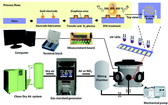
Fig. 1 shows the gas sensing measurement setup including the gas concentration generator and electrical measurement. The sensor was placed in the test chamber with a volume of 3 liters and an array of 4 UV light-emitting diodes (LEDs) (370 nm, maximum power 70 mW, KOODYZ) was fixed at a distance of 5 mm from the top of the sensor surface. This UV light (370 nm wavelength) can allow graphene remain with fewer defects as the energy is not sufficient for bond breaking or graphene oxidation by ozone.26 The UV LED array was connected to a power supply (3 V) for illumination. The flow rates of dry air and target gas were controlled by mass flow controllers to introduce the target gas at different concentrations to the test chamber. The accurate concentration could be controlled by the NO2 emission in the gas standards generator (FlexStream™ Base Module, KIN-TEK Laboratories Inc, USA). The gas sensing response was monitored by the change in resistance caused by gas molecule adsorption on the graphene surface. A 4-channel readout system constructed by inverting amplifier circuit could be used to filter noises and convert to the resistance signal. The resistance values were recorded by DAQ card setting and self-developed LabVIEW program.2.3 Material analysis
The spatially resolved maps of the G and 2D bands of all the samples were obtained using a Raman microscope system (UniDRON, CL Technology Co., Ltd., Taiwan) with an excitation laser at a wavelength of 473 nm. The spot size of the laser was 0.5 μm. The Raman scattering peak of Si at 520 cm−1 was used as reference for wavenumber calibration before all measurements. The result of Raman spectra could be used to identify the characteristics of graphene including quality, number of layers, strain and doping.27–29 To measure the Hall-effect mobility and hole concentration, four silver balls were fabricated on the graphene surface with the same distance.30 A Hall measurement system (Bio-Rad HL5500, Nanometrics, U.S.) with a magnetic field of 0.5 T was used to obtain the carrier mobility and concentrations. The AFM images were collected by a Cypher ES model from Asylum Research Oxford Instrument operating in tapping mode to scan the surface roughness of graphene. The scanning rate was 1 Hz with 512 scanning lines.2.4 NO2 sensing measurements and UV illumination
Before starting measurements, the mechanical pump separately evacuated the test chamber and mixing chamber to 10−3 Torr to get the initialized state. A mass flow controller was used to modulate the flow rate of air to dilute the NO2 concentration from the permeation tube with a fixed emission rate. By this method, the selected concentration of NO2 can be obtained for sensor characterization. This target amount of NO2 was generated by the gas generator and injected into the mixing chamber until reaching a pressure of 9 × 10² Torr for the gas storage. Then, this gas was injected into the test chamber by a valve and mass flow controller, reaching a pressure of 7 × 10² Torr for measurement. Total of 4 sensors with the same group were measured for all NO2 concentrations to evaluate the sensor variation. The exposure time was 15 min for the sensor to detect the target gas. The same protocol was defined for the injection of different concentrations of NO2. During the desorption process, the test chamber was first pumped out by a mechanical pump; after pumping out for 2 min to a residual gas pressure of 10−2 Torr, the UV LED array was illuminated to enhance the removal of the residual gas molecules from the graphene surface. The resistance of the sensor could increase during this period to reach its initial value. Then, the UV LED array was turned off and the test chamber was pumped out for a total of 15 min. The chamber was cleaned by following the previously described procedures between different cycles of NO2 introduction to ensure the same initial condition.3. Results and discussion
3.1 Graphene characterization
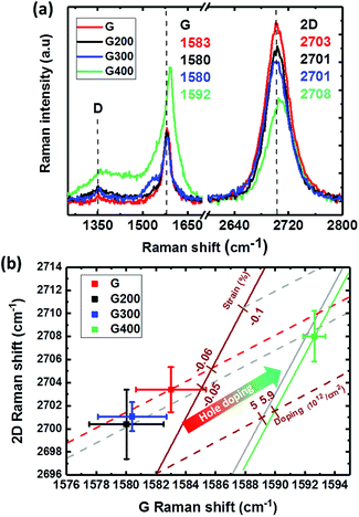
Raman analysis is widely used to characterize the structure of graphene, crystalline quality and doping. The G peak (∼at 1585 cm−1) and 2D peak (∼at 2700 cm−1) are characteristics of the C–C bonds with sp2-hybridized in graphene. The D band (∼at 1350 cm−1) is mostly related with the lattice disorder or density of defects.31 As shown in Fig. 2(a), the Raman spectra for the sample “G” shows no significant peak in the D band region, indicating few defects. The ratio of the intensities of the G peak and 2D peak is about 2.4 and the full-width-at-half-maximum (FWHM) of the 2D peak is 38 cm−1, which could be used to conclude the graphene structure to be a monolayer. The annealed sample at 400 °C (sample of “G400”) shows broad peaks between the G and D peaks, suggesting increased disorder in graphene and amorphous carbon formation from the degradation of PMMA residue on the sample surface.32 In addition, both 2D and G bands show a clear blue shift at the RTA temperature of 400 °C as seen previously for RTA-treated samples.20 This can result from the hole doping induced by O2 from the bottom SiO2 or by activated reaction with atmospheric O2 at this temperature.20,33In order to further confirm the effect of hole doping and the strain effect induced by RTA, G and 2D band shifts at various annealing temperatures in the Raman spectra were collected for 5 points. The correlation plot of the G band shift and 2D band shift is redrawn as shown in Fig. 2(b). The excitation energy of 2.33 eV for the 532 nm wavelength used in Raman spectrum results in pristine graphene (without doping and strain) G and 2D band peaks at 1582 and 2670 cm−1, respectively.34 The G band peak of pristine graphene will not change, but the 2D band could be shifted by different energy of the excitation laser.35,36 The 2D band peak of pristine graphene could be shifted to 2695 cm−1 since the high energy of excitation from the laser wavelength of 473 nm in our experiment and the corresponding exchange ratio of 88 cm−1 eV−1.36 A new reference baseline with a slope of 2.45 (brown solid line) and 0.7 (brown dash line) initiated from this point can be used to identify the strain and doping effects, respectively.37 The units of these new coordination for percentage of strain (ε) and hole concentration from doping (p) could be defined as % and 1012 cm−2, respectively. The evaluation of doping level is from the data presented by Das et al.38 to create the new coordination of doping line.37 A slope of −57 cm−1/1% could be used to calculate the strain (%) based on the G band shift, which is derived from the Grüneisen parameters for graphene under uniaxial or biaxial strain.39 Some reference lines marked in brown color are shown in Fig. 2(b). The level of strain and doping could be obtained by the intersections of the fitting line of each group.40,41 By using this method and new coordination, the shift of G band of the “G” group project to the strain axis at a strain value of −0.06% as shown in the red arrow dash line in Fig. 2(b); this could be due to the water molecules or PMMA residue on the graphene surface and strain during the transfer process.42 The G and 2D bands are both slightly red-shifted at RTA temperatures of 200 and 300 °C, indicating graphene with less compressive strain and a reduction in hole doping. This could be contributed by graphene suffering tensile strain from the glass substrate due to the difference in their thermal expansion coefficients and electron doping from the degradation of PMMA.43,44 With temperature increasing to 400 °C, the doping obviously changed to heavily p-type with a concentration of 5.9 × 1012 cm−2. Hole doping by oxygen from glass substrate has been reported previously at an RTA temperature of 400 °C in N2,45 in addition to hole doping by annealing from 400 to 600 °C.46 The RTA with a fast heating rate followed by cooling down to room temperature within few minutes can induce thermal expansion coefficient mismatch between graphene and the glass substrate, which can cause compressive strain and hole doping on graphene.47
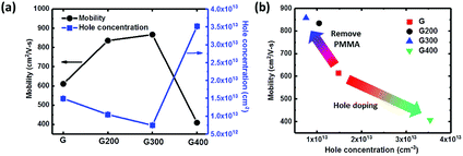
The doping effect by RTA treatment at various temperatures is also studied by the measurement of Hall mobility and carrier concentration with different rotation angle of 0°, 90°, 180° and 270°. As shown in Fig. 3(a), graphene without annealing shows a hole concentration of 1.48 × 1013 cm−2, and this natural p-type doped behavior could be contributed from the adsorbed oxygen and water molecules in atmosphere. When RTA temperature increases to 300 °C, the Hall mobility increases significantly from 613 to 859 cm2 V−1 s−1 and the natural p-type doped graphene becomes intrinsic with the hole concentration decreasing. Thus, RTA treatment is useful to restore the intrinsic properties and remove PMMA residues from the graphene surface to improve carrier transport. As annealing temperature increases to 400 °C, the Hall mobility decreases to 405 cm2 V−1 s−1 and the hole concentration of graphene increases to 3.5 × 1013 cm−2, which could be from hole doping by oxygen from the bottom glass substrate. Hall effect could be a useful indicator for various dopants to graphene including AuCl3, HNO3, and ozone as shown in previous studies.48 Fig. 3(b) shows a plot of mobility versus hole concentration for various RTA temperatures. The samples annealed at 200 and 300 °C show a higher Hall mobility and less hole concentration due to PMMA residue removal. In contrast, the 400 °C sample presents an opposite trend consistent with the Raman spectrum presented in Fig. 2(b).
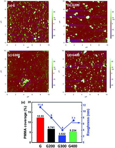
The surface roughness of the graphene surface was investigated by AFM images as shown in Fig. 4 in order to further confirm the removal of PMMA residues by RTA. Some PMMA residues are still seen on the graphene surface even after the supporting layer of PMMA was immersed in the acetone solution for 1 hour as shown in Fig. 4(a). After the RTA treatment, the efficiency of removing PMMA residues is clearly observed in Fig. 4(b) and (c). When the RTA temperature increases to 400 °C, the surface roughness slightly increases compared to 300 °C as seen in Fig. 4(d). Fig. 4(e) shows the root mean square roughness (Rq) value of the RTA-treated graphene layer. The Rq value decreases with increasing temperature up to 300 °C, but increases to 7.1 nm at 400 °C. The elimination of PMMA film at annealing temperature of 300 °C can also be supported by thermogravimetric analysis.49 The forming of amorphous carbon by RTA at 400 °C21 can be the source of carbon atoms from the PMMA residues. This phenomenon can also be supported by the broadening of G and 2D peaks in the Raman spectra.32 More importantly, the distribution of PMMA residues would block the gas molecules from the graphene surface.23 In addition, the surface roughness of mechanical exfoliation graphene on the SiO2 substrate is only 0.154 nm,50 which means the Rq value is mostly from the surface residues of PMMA. AFM images were further analyzed by using ImageJ software to quantify the ratio of PMMA coverage. All AFM images are replotted by setting a new threshold value of roughness to define the PMMA area as shown in Fig. S1(a) to (d).† The calculated percentage of residue coverage in the pristine graphene is 19.53%, 6.741%, 3.532% and 5.234% for the samples annealed at 200 °C, 300 °C and 400 °C respectively. The graphene surface coverage and the graphene domain size were also evaluated in the same way.51
Based on the above results of Raman spectrum, Hall measurement and surface roughness by AFM, the PMMA could be almost removed at an RTA temperature of 300 °C. The RTA temperature at 400 °C could form amorphous carbon on the graphene surface leading to a high surface roughness.
3.2 NO2 gas sensing performance
The dynamic response of the resistance relative to different concentrations of NO2 diluted in dry air was measured in series as the standard protocol. The NO2 concentrations in this protocol were 0, 1, 3 and 5 ppm in a series of administrations of the gas. For the recovery step, a mechanical pump was used first to remove the residual gas in the test chamber for 15 min before each cycle of NO2 detection. The sensor response and recovery are defined as the relative change of resistance by exposure to or removal from a given gas concentration:
 | (1) |
 | (2) |
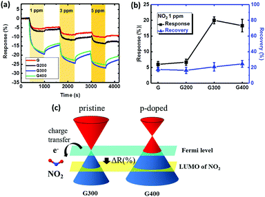
Fig. 5(a) shows the dynamic responses of the sensor with graphene annealed at various temperatures. Injection of 1 ppm NO2 to the “G” sensor reduces the resistance quickly with a 6% change. NO2 is a strong oxidizing gas, transferring electrons from the graphene surface, which makes graphene a p-type-doped layer and is followed by a decrease in resistivity. The response of the 300 °C is higher (up to 20%) compared to the “G” sensor as removing the PMMA residue can create more surface area for adsorption. With NO2 injection on the graphene surface with fewer residues of PMMA, more sensing area of graphene can be used to adsorb NO2 molecules on the surface and more charges transferred to the graphene. According to this mechanism, the sensor with the RTA treatment at 300 °C provided higher response due to the minimum amount of PMMA residue on the graphene as supported by the AFM results. Furthermore, the method of RTA could be suggested as a pretreatment to remove residues before other surface modifications for different applications.52–55 Fig. 5(b) shows the absolute value of the sensor response and recovery for 1 ppm NO2. The absolute value of the response for the “G”, “G200”, “G300” and “G400” sensors is 6%, 6.7%, 20% and 18.3%. The best response is for the 300 °C annealed case and the response is slightly degraded with RTA temperature of 400 °C. There are two effects involved in determining the sensing performance at RTA temperature of 400 °C. First, the amorphous carbon formation on the graphene surface discussed earlier can block NO2 adsorption leading to lower response. Second, the hole doping occurring at 400 °C modifies the energy band and the Dirac point of graphene is higher than the Fermi level as shown in Fig. 5(c).56 During the NO2 adsorption, the Fermi level of p-doped and pristine graphene decreases until alignment with the lowest unoccupied molecular orbital (LUMO) of NO2, meaning that p-doped graphene enjoys more electron transfer to NO2. Thus, the NO2 response is still similar to that annealed at 300 °C even with amorphous carbon formation on the graphene surface at 400 °C.
Regarding sensor recovery, all sensors show a recovery less than 25% after the 1 ppm exposure. With this poor recovery, the sensor response degraded in the second cycle when exposed to 3 ppm because the site coverage on the graphene surface is still high from the previous cycle. The strong adsorption energy of NO2 on graphene is confirmed by the density of states (DOS),57 leading to the poor recovery behavior at 3 and 5 ppm. In summary, the NO2 response of the sensors can be improved by RTA but the issue of poor recovery remains unsolved.
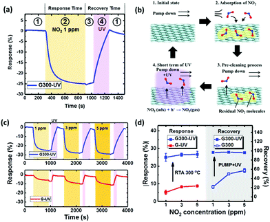
In order to improve this poor recovery behavior, a short-time UV illumination on the graphene surface during the pump down process is applied with the advantages of low power consumption in an efficient way.58 As shown in Fig. 6(a), the recovery of the “G300” sensor could be fully recovered to the original baseline by UV illumination for 4 min and pumping down in the recovery step. This operation of one cycle can be separated into four steps as follows: first, the sensor was in the vacuum environment during pump down, keeping the response stable (stage ①). The second step involves stopping pump down and injecting 1 ppm NO2 until the response saturates (stage ②). Third, pumping for 2 min as a pre-cleaning process to reduce the residual NO2 in the environment and potential ozone damage to graphene by UV illumination (stage ③). Finally, the UV LED array is turned on to aid gas desorption from the graphene surface until the resistance returns to the baseline level (stage ④). The mechanism for this procedure of UV illumination and pumping down for a better recovery is illustrated in Fig. 6(b). In stage ①, no additional gas molecules could reach the graphene surface in the vacuum environment. In stage ②, the injected NO2 molecules adsorb on the surface. In stage ③, the pumping down process was used to remove the residual gas from the measurement environment. Finally, the UV light was turned on to make graphene generate the electron–hole pairs. This phenomenon follows NO2− (ads) + h+ → NO2 (gas), leading to full desorption from the graphene surface under UV illumination to the initial state. The advantage of this proposed 2-step recovery including pumping down and UV illumination is less UV-ozone generation and less defects on the graphene making it suitable for long-term and precise sensing applications.26,59
The illumination time needed for recovery was investigated in detail for various conditions. The recovery of the RTA-treated sensors is lower than with illumination time for optimization of the “G” sensor as shown in Fig. S2(a).† The graphene surface with RTA treatment has more sensing sites as mentioned earlier to adsorb NO2 molecules, leading to incomplete desorption in a short-time UV illumination. When the UV illumination time is extended for the full recovery of the sensor RTA-treated at 300 °C (Fig. S2(b)†), the highest response change is achieved at 300 °C for concentrations from 1 to 5 ppm. In particular, the percentage recovery for both “G” and “G200” is higher than 100%. This phenomenon can presumably be ascribed to the presence of oxygen and water molecules on the graphene in the initial state, followed by desorption with UV illumination. The sensing performance of the “G” and “G300” sensors with optimized UV illumination time is shown in Fig. 6(c). The “G300” sensor shows a higher response change than the “G” sensor for all the concentrations. The time of UV illumination for “G300” sensor increases from 110 to 400 s compared to the “G” sensor due to more NO2 molecules adsorbed on the graphene surface. Fig. 6(d) presents the absolute values of the response change and recovery by UV illumination for various NO2 concentrations. The NO2 response improves from 5.3% to 20% for the RTA temperature at 300 °C for 1 ppm. The recovery for various concentrations can be significantly improved to more than 90% compared to the case without UV illumination. These results show that the combination of RTA treatment and UV illumination has potential for a gas sensor with high response and short time recovery. To evaluate the stability and repeatability, the sensors “G” and “G300” were tested 3 cycles for 1 ppm NO2 concentration as shown in Fig. S3.† A good repeatability is seen from the variation of response within 0.6% and 0.3% for the two sensors respectively. In addition, after UV illumination on graphene for 3 h in a vacuum environment, no additional defects can be observed by Raman spectra as shown in Fig. S4.† According to the above, the number of cycles with sustained sensing can be more than 12 by the total illumination time of 3 h divided by the UV illumination time of 15 min for recovering the concentration of 5 ppm. Therefore, the damage to graphene must be negligible from the illumination effect. For practical applications using this proposed UV illumination, an automatic system with a program to control the switch of the UV light source can be designed for fast recovery to baseline, which can be an example for the combination of smart sensors and internet of things (IoT). Besides, the micropump integrated with a microfluidics channel on the chip of gas sensor is a feasible way to replace the original system including the mechanical pump, the mixer chamber and the test chamber for the purpose of miniaturization.60
We also investigated the response properties of RTA treatment on the sensor for various gases at room temperature. Fig. 7 shows the response and recovery of “G” and “G300” sensors to pure air, CH3CH2OH of 1 ppm, NH3 of 5 ppm and NO2 of 1 ppm. Obviously, the “G300” sensor showed a clearly large change in response for NO2, which was negative and more than 4 times higher than those of the other gases. In addition, all the gas response can be improved by RTA treatment due to the removal of PMMA residues. These results show that the “G300” sensor has a good selectivity to NO2 at room temperature, which can be a candidate for NO2 gas sensing in environmental monitoring systems. A comparison between the sensing performances of this proposed sensor and other NO2 sensors based on graphene is summarized in Table 1.10,61–65 We found that the effect of RTA treatment and UV illumination on monolayer graphene in this study could be used to detect NO2 in the concentration range from 1 to 5 ppm with a complete recovery within 900 s at room temperature, which is better than other NO2 sensors and suitable for long-term and precise sensing applications.
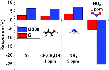 | ||
| Fig. 7 Gas responses of the “G” and “G300” sensors exposed to pure air, CH3CH2OH of 1 ppm, NH3 of 5 ppm and NO2 of 1 ppm at room temperature. | ||
| Sensing materials | NO2 response | Operation temp. (°C) | Recovery time (s) | Recovery | Ref. |
|---|---|---|---|---|---|
| 4AQ-rGO | 60% at 1 ppm | RT | 3300 | 80% | 10 |
| MoS2/rGO | 12% at 0.15 ppm | 90 °C | 300 | 40% | 61 |
| RGONMF | 15% at 1 ppm | RT | 5000 | 60% | 62 |
| CVD-Gr | 4% at 1.5 ppm | 22 °C | 1800 | 50% | 63 |
| RGO | 30% at 1 ppm | RT | 3000 | 70% | 64 |
| g-C3N4/graphene | 40% at 20 ppm | RT | 1200 | 60% | 65 |
| Graphene | 20% at 1 ppm | RT | 900 | 97% | This work |
4. Conclusions
NO2 sensing characteristics for graphene with RTA treatment and UV illumination are presented in this study. The sensor response is improved by 4 times with RTA treatment at 300 °C. Removal of PMMA residues from the graphene surface by RTA treatment leads to more NO2 molecular adsorption. Complete recovery can be achieved with proper UV illumination by the control of irradiation time. Therefore, the optimization of RTA treatment and UV illumination of graphene-based sensor could be useful for ppb level sensing of NO2.Conflicts of interest
There are no conflicts to declare.Acknowledgements
This work was supported in part by the Ministry of Science and Technology of the Republic of China under the Contract no. of MOST 106-2632-E-182-001 and 105-2221-E-182-057-MY3 and the Chang Gung Memorial Hospital under the contracts of CMRPD2G0202, CMRPD2I0011 and CMRPD2F0063.References
- D. Zhang, Z. Liu, C. Li, T. Tang, X. Liu, S. Han, B. Lei and C. Zhou, Nano Lett., 2004, 4, 1919–1924 CrossRef CAS.
- A. P. F. Turner and N. Magan, Nat. Rev. Microbiol., 2004, 4, 161–166 CrossRef PubMed.
- Y. H. Navale, S. T. Navale, F. J. Stadler, N. S. Ramgir and V. B. Patil, Ceram. Int., 2019, 435, 1513–1522 CrossRef.
- R.-A. Wu, C. W. Lin and W. J. Tseng, Ceram. Int., 2017, 43, 535–540 CrossRef.
- M. Meyyappan, Small, 2016, 12, 2118–2129 CrossRef CAS PubMed.
- J. Li, Y. Lu, Q. Ye, M. Cinke, J. Han and M. Meyyappan, Nano Lett., 2003, 3, 929–933 CrossRef CAS.
- A. K. Geim, Science, 2009, 324, 1530–1534 CrossRef CAS PubMed.
- R. Pearce, T. Iakimov, M. Andersson, L. Hultman, A. L. Spetz and R. Yakimova, Sens. Actuators, B, 2011, 155, 451–455 CrossRef CAS.
- F. Schedin, A. K. Geim, S. V. Morozov, E. W. Hill, P. Blake, M. I. Katsnelson and K. S. Novoselov, Nat. Mater., 2007, 6, 652–655 CrossRef CAS PubMed.
- R. Jia, P. Xie, Y. Feng, Z. Chen, A. Umar and Y. Wang, Appl. Surf. Sci., 2018, 440, 409–414 CrossRef CAS.
- G. Chen, T. M. Paronyan and A. R. Harutyunyan, Appl. Phys. Lett., 2012, 101, 053119 CrossRef.
- M. Kodu, A. Berholts, T. Kahro, T. Avarmaa, A. Kasikov, A. Niilisk, H. Alles and R. Jaaniso, Appl. Phys. Lett., 2016, 109, 113108 CrossRef.
- M. Shafiei, J. Bradford, H. Khan, C. Piloto, W. Wlodarski, Y. Li and N. Motta, Appl. Surf. Sci., 2018, 462, 330–336 CrossRef CAS.
- A. K. Singh, M. A. Uddin, J. T. Tolson, H. Maire-Afeli, N. Sbrockey, G. S. Tompa, M. G. Spencer, T. Vogt, T. S. Sudarshan and G. Koley, Appl. Phys. Lett., 2013, 102, 043101 CrossRef.
- O. Ovsianytskyi, Y.-S. Nam, O. Tsymbalenko, P.-T. Lan, M.-W. Moon and K.-B. Lee, Sens. Actuators, B, 2018, 257, 278–285 CrossRef CAS.
- F. Günes, H. Arezki, D. Pierucci, D. Alamarguy, J. Alvarez, J.-P. Kleider, Y. J Dappe, A. Ouerghi and M. Boutchich, Nanotechnology, 2015, 26, 445702 CrossRef PubMed.
- A. Ambrosi, A. Bonanni, Z. Sofer and M. Pumera, Nanoscale, 2013, 5, 2379–2387 RSC.
- G. Deokar, J. Avila, I. Razado-Colambo, J.-L. Codron, C. Boyaval, E. Galopin, M.-C. Asensio and D. Vignaud, Carbon, 2015, 89, 82–89 CrossRef CAS.
- R. Sachs, Z. Lin, P. Odenthal, R. Kawakami and J. Shi, Appl. Phys. Lett., 2014, 104, 033103 CrossRef.
- C. W. Jang, J. H. Kim, J. M. Kim, D. H. Shin, S. Kim and S.-H. Choi, Nanotechnology, 2013, 24, 405301 CrossRef PubMed.
- B. Liu, I.-S. Chiu and C.-S. Lai, Vacuum, 2017, 137, 8–13 CrossRef CAS.
- K. Alexandrou, F. Farmakis, A. Arapis, N. Georgoulas, Y. Hao, J. Hone and I. Kymissis, J. Vac. Sci. Technol., B: Nanotechnol. Microelectron.: Mater., Process., Meas., Phenom., 2016, 34, 041805 Search PubMed.
- J. Hong, S. Lee, J. Seo, S. Pyo, J. Kim and T. Lee, ACS Appl. Mater. Interfaces, 2015, 7, 3554–3561 CrossRef CAS PubMed.
- C.-M. Yang, T.-C. Chen, Y.-C. Yang, M.-C. Hsiao, M. Meyyappan and C.-S. Lai, Vacuum, 2017, 140, 89–95 CrossRef CAS.
- M. T. Ghoneim, C. E. Smith and M. M. Hussain, Appl. Phys. Lett., 2013, 102, 183115 CrossRef.
- F. Gunes, G. H. Han, H.-J. Shin, S. Y. Lee, M. Jin, D. L. Duong, S. J. Chae, E. S. Kim, F. Yao, A. Benayad, J.-Y. Choi and Y. H. Lee, Nano: Brief Reports and Reviews, 2011, 6(05), 409–418 CrossRef.
- X. Yang, M. Zhang, J. Zheng, W. Li, W. Gan, J. Xu, T. Hayat, N. S. Alharbi and F. Yang, Appl. Surf. Sci., 2018, 439, 128–138 CrossRef CAS.
- B. Liu, Z. Liu, I.-S. Chiu, M. F. Di, Y. R. Wu, J.-C. Wang, T.-H. Hou and C.-S. Lai, ACS Appl. Mater. Interfaces, 2018, 10, 20237–20243 CrossRef CAS PubMed.
- B. Liu, C.-M. Yang, Z. Liu and C.-S. Lai, Nanomaterials, 2017, 7, 302 CrossRef PubMed.
- Z. Wang, M. Shaygan, M. Otto, D. Schall and D. Neumaier, Nanoscale, 2016, 8, 7683–7687 RSC.
- S. D. Sarma, S. Adam, E. H. Hwang and E. Rossi, Rev. Mod. Phys., 2011, 83, 407–470 CrossRef.
- C. Gong, H. C. Floresca, D. Hinojos, S. McDonnell, X. Qin, Y. Hao, S. Jandhyala, G. Mordi, J. Kim and L. Colombo, J. Phys. Chem. C, 2013, 117, 23000–23008 CrossRef CAS.
- A. Nourbakhsh, M. Cantoro, A. Klekachev, F. Clemente, B. Sorée, M. H. van der Veen, T. Vosch, A. Stesmans, B. Sels and S. D. Gendt, J. Phys. Chem. C, 2010, 114, 6894–6900 CrossRef CAS.
- T. G. A. Verhagen, K. Drogowska, M. Kalbac and J. Vejpravova, Phys. Rev. B: Condens. Matter Mater. Phys., 2015, 92, 125437 CrossRef.
- O. Frank, J. Vejpravova, V. Holy, L. Kavan and M. Kalbac, Carbon, 2014, 68, 440–451 CrossRef CAS.
- D. L. Mafra, G. Samsonidze, L. M. Malard, D. C. Elias, J. C. Brant, F. Plentz, E. S. Alves and M. A. Pimenta, Phys. Rev. B: Condens. Matter Mater. Phys., 2007, 76, 233407 CrossRef.
- J. E. Lee, G. Ahn, J. Shim, Y. S. Lee and S. Ryu, Nat. Commun., 2012, 3, 1024 CrossRef PubMed.
- A. Das, B. Chakraborty, S. Piscanec, S. Pisana, A. K. Sood and A. C. Ferrari, Phys. Rev. B: Condens. Matter Mater. Phys., 2009, 79, 155417 CrossRef.
- T. M. G. Mohiuddin, A. Lombardo, R. R. Nair, A. Bonetti, G. Savini, R. Jalil, N. Bonini, D. M. Basko, C. Galiotis, N. Marzari, K. S. Novoselov, A. K. Geim and A. C. Ferrari, Phys. Rev. B: Condens. Matter Mater. Phys., 2009, 79, 205433 CrossRef.
- A. Armano, G. Buscarino, M. Cannas, F. M. Gelardi, F. Giannazzo, E. Schilirò and S. Agnello, Carbon, 2018, 127, 270–279 CrossRef CAS.
- A. Piazza, F. Giannazzo, G. Buscarino, G. Fisichella, A. L. Magna, F. Roccaforte, M. Cannas, F. M. Gelardi, B. Pignataro, M. Scopelliti and S. Agnello, Carbon, 2016, 107, 696–704 CrossRef CAS.
- B. H. Son, H. S. Kim, H. Jeong, Ji-Y. Park, S. Lee and Y. H. Ahn, Sci. Rep., 2017, 7, 18058 CrossRef CAS PubMed.
- X. Zheng, W. Chen, G. Wang, Y. Yu and S. Qin, AIP Adv., 2015, 5, 057133 CrossRef.
- C. Deng, W. Lin, G. Agnus, D. Dragoe, D. Pierucci, A. Ouerghi, S. Eimer, I. Barisic, D. Ravelosona, C. Chappert and W. Zhao, J. Phys. Chem. C, 2014, 118, 13890–13897 CrossRef CAS.
- S. Suzuki, C. M. Orofeo, S. Wang, F. Maeda, M. Takamura and H. Hibino, J. Phys. Chem. C, 2013, 117, 22123–22130 CrossRef CAS.
- J. Kang, D. Shin, S. Baea and B. H. Hong, Nanoscale, 2012, 4, 5527–5537 RSC.
- D. Yoon, Y.-W. Son and H. Cheong, Nano Lett., 2011, 11, 3227–3231 CrossRef CAS PubMed.
- M. Hofmann, Y.-P. Hsieh, K.-W. Chang, H.-G. Tsai and T.-T. Chen, Sci. Rep., 2015, 5, 17393 CrossRef CAS PubMed.
- J. Zheng, M. Zhang, T. Miao, J. Yang, J. Xu, N. S. Alharbi and M. Wakeel, Mater. Chem. Front., 2019, 3, 224–232 RSC.
- C. H. Lui, L. Liu, K. F. Mak, G. W. Flynn and T. F. Heinz, Nature, 2009, 462, 339–341 CrossRef CAS PubMed.
- S. Chaitoglou, E. Pascual, E. Bertran and J. L. Andujar, J. Nanomater., 2016, 2016, 9640935 Search PubMed.
- F. Perreault, A. F. d. Faria and M. Elimelech, Chem. Soc. Rev., 2015, 44, 5861–5896 RSC.
- H. Zhao, S. Fan, Y. Chen, Z. Feng, H. Zhang, W. Pang, D. Zhang and M. Zhang, ACS Appl. Mater. Interfaces, 2017, 9, 40774–40781 CrossRef CAS PubMed.
- J.-C. Wang, K.-P. Chang, C.-T. Lin, C.-Y. Su, F. Gunes, M. Boutchich, C.-H. Chen, C.-H. Chen, C.-S. Chen, L.-J. Li and C. S. Lai, Carbon, 2017, 113, 318–324 CrossRef CAS.
- T. Hu and I. C. Gerber, J. Phys. Chem. C, 2013, 117, 2411–2420 CrossRef CAS.
- K. S. Mali, J. Greenwood, J. Adisoejoso, R. Phillipson and S. D. Feyter, Nanoscale, 2015, 7, 1566 RSC.
- X. Lin, J. Ni and C. Fang, J. Appl. Phys., 2013, 113, 034306 CrossRef.
- C.-M. Yang, T.-C. Chen, Y.-C. Yang, M. Meyyappan and C.-S. Lai, Sens. Actuators, B, 2017, 253, 77–84 CrossRef CAS.
- Y. C. Cheng, T. P. Kaloni, Z. Y. Zhu and U. Schwingenschlögl, Appl. Phys. Lett., 2012, 101, 073110 CrossRef.
- M. Paknahad, J. S. Bachhal, A. Ahmadi and M. Hoorfar, Sens. Actuators, B, 2017, 241, 55–64 CrossRef CAS.
- H. J. Park, W.-J. Kim, H.-K. Lee, D.-S. Lee, J.-H. Shin, Y. Jun and Y. J. Yun, Sens. Actuators, B, 2018, 257, 846–852 CrossRef CAS.
- F. Ricciardella, S. Vollebregt, T. Polichetti, M. Miscuglio, B. Alfano, M. L Miglietta, E. Massera, G. Di Francia and P. M. Sarro, Nanoscale, 2017, 9, 6085–6093 RSC.
- Y. J. Yun, D. Y. Kim, W. G. Hong, D. H. Ha, Y. Jun and H.-K. Lee, RSC Adv., 2018, 8, 7615–7621 RSC.
- S. Zhang, N. T. Hang, Z. Zhang, H. Yue and W. Yang, Nanomaterials, 2017, 7, 12 CrossRef PubMed.
- R. Jia, P. Xie, Y. Feng, Z. Chen, A. Umar and Y. Wang, Appl. Surf. Sci., 2018, 440, 409–414 CrossRef CAS.
Footnotes |
| † Electronic supplementary information (ESI) available. See DOI: 10.1039/c9ra01295h |
| ‡ C.-M. Yang and T.-C. Chen contributed equally to this work. |
| This journal is © The Royal Society of Chemistry 2019 |

