
 Open Access Article
 This Open Access Article is licensed under a Creative Commons Attribution-Non Commercial 3.0 Unported Licence
Interfacial electronic structure between a W-doped In2O3 transparent electrode and a V2O5 hole injection layer for inorganic quantum-dot light-emitting diodes
Su Been Heoa,
Jong Hun Yua,
Minju Kimb,
Yeonjin Yib,
Ji-Eun Leec,
Han-Ki Kim c and
Seong Jun Kang*a
c and
Seong Jun Kang*a
aDepartment of Advanced Materials Engineering for Information and Electronics, Kyung Hee University, 1732 Deogyeong-daero, Giheung-gu, Yongin, Gyeonggi-do 17104, Republic of Korea. E-mail: junkang@khu.ac.kr; Tel: +82-31-201-3324
bInstitute of Physics and Applied Physics, Yonsei University, 50 Yonsei-ro, Seodaemun-gu, Seoul 03722, Republic of Korea
cSchool of Advanced Materials & Engineering, Sungkyunkwan University, 2066 Seobu-ro, Jangan-gu, Suwon, Gyeonggi-do 16419, Republic of Korea
First published on 16th April 2019
Abstract
The interfacial electronic structure between a W-doped In2O3 (IWO) transparent electrode and a V2O5 hole injection layer (HIL) has been investigated using ultraviolet photoelectron spectroscopy for high-performance and inorganic quantum-dot light-emitting diodes (QLEDs). Based on the interfacial electronic structure measurements, we found gap states in a V2O5 HIL at 1.0 eV below the Fermi level. Holes can be efficiently injected from the IWO electrode into poly[(9,9-dioctylfluorenyl-2,7-diyl)-co-(4,4′-(4-sec-butylphenyl)diphenylamine)] (TFB) through the gap states of V2O5, which was confirmed by the hole injection characteristics of a hole-only device. Therefore, conventional normal-structured QLEDs were fabricated on a glass substrate with the IWO transparent electrode and V2O5 HIL. The maximum luminance of the device was measured as 9443.5 cd m−2. Our result suggests that the IWO electrode and V2O5 HIL are a good combination for developing high-performance and inorganic QLEDs.
Introduction
Light-emitting diodes based on electroluminescence from quantum-dots are one of the most promising devices as next-generation displays due to the narrow emission spectrum characteristics and the high luminous efficiency.1–3 Quantum-dot light-emitting diodes (QLEDs) can be fabricated using a low-cost solution process that enables a large-scale flexible display.4 Moreover, the band gap of quantum-dots (QDs) is controllable by changing the dimensions of QDs due to the quantum confinement effect.5 Therefore, full-color QLEDs and white QLEDs have been successfully demonstrated.6–8Conventional indium-tin-oxide (ITO) film is the most commonly used transparent electrode for light-emitting diodes and photovoltaics.9,10 Sputtered ITO films have a low sheet resistance and high carrier mobility with a high carrier concentration.11 Although a high process temperature (300 °C) is required to form an ITO film with a high conductivity, ITO is a typical transparent electrode to fabricate QLEDs.12 Generally, ITO is used as a transparent electrode and poly (3,4-ethylenedioxythiophene):poly (styrenesulfonate) (PEDOT:PSS) is used as a hole injection layer (HIL) for the QLEDs.13 However, the hygroscopic and acidic nature of PEDOT:PSS can damage the surface of the ITO, and degrade device performance parameters such as the electroluminescence (EL) and life-time of the device.14 Therefore, ITO and PEDOT:PSS is not a good combination for stable and high-performance QLEDs. Recently, several attempts to replace ITO in optoelectronics were made. The candidates to replace ITO are Al-doped ZnO, Ti-doped In2O3, and W-doped In2O3 (IWO) due to the desirable properties of high mobility, low sheet resistance, and high transmittance.15–17 Among the alternatives to ITO, IWO is considered as a suitable transparent electrode for the QLEDs. Tungsten (W) dopants in the In2O3 can generate an abundance of electron carriers due to the W6+ substitutions in the In3+ sites.18 As a result, the IWO requires less dopant than ITO, which can improve the impurity scattering effect. Therefore, IWO films can have a higher carrier concentration and higher mobility than ITO films. Moreover, the fabrication temperature for the highly transparent and conductive IWO film is lower than that of the ITO film.19
Meanwhile, there are many reports to suggest an alternative to PEDOT:PSS in QLEDs. Transition metal oxides (TMOs) are proposed as an HIL for the device because TMOs do not have acidic and hygroscopic properties. TMOs films may be formed using a solution coating process as well as the vacuum sputtering process. Vanadium oxide (V2O5), molybdenum oxide (MoO3), nickel oxide (NiO), and copper oxide (CuO) have been used as a HIL in QLEDs.20–23 QLEDs with TMOs as the HIL exhibited superior characteristics including stability upon exposure to oxygen, hydrogen, and heat.24 Also, the adhesion force of V2O5 is strong enough to form a stable thin film on a substrate.25 Therefore, the IWO transparent electrode and V2O5 HIL could be a suitable combination for developing the high-performance and inorganic QLEDs.
In this study, we fabricated inorganic QLEDs with the IWO transparent electrode and V2O5 HIL. The hole injection mechanism from the IWO electrode into the V2O5 HIL was investigated using ultraviolet photoelectron spectroscopy (UPS), and we found gap states inside the band gap of V2O5. The gap states can provide a hole carrier injection pathway through the wide band gap of the V2O5 HIL. The hole injection characteristics between the IWO and V2O5 was investigated by characterizing a hole-only device (HOD), and efficient hole injection was observed. Conventional normal-structured QLEDs were fabricated successfully on a glass substrate with the IWO transparent electrode and V2O5 HIL. Our result suggests that the IWO transparent electrode and V2O5 HIL could be a good combination for the production of high-performance and inorganic QLEDs.
Experiments
We fabricated conventional-structured QLED devices on IWO electrodes with inorganic V2O5 HILs. A 100 nm thick layer of IWO films were deposited on a glass substrate using a plot-scale ion plating system with IWO tablets (99 at% In2O3 – 1 at% W) at room temperature.26 During deposition of the IWO film, the working pressure, DC power and Ar/O2 flow rate were constantly maintained at 3 mTorr, 3000 W and 300/90 sccm, respectively.18 The V2O5 solution was prepared using vanadium oxitriisopropoxide (Alfa Aesar, 96%) and isopropyl alcohol at a volume ratio of 1![[thin space (1/6-em)]](https://www.rsc.org/images/entities/char_2009.gif) :70.20 The V2O5 HIL was spin-coated on the IWO surface at 3000 rpm for 30 s, followed by annealing at 150 °C for 30 min. Then poly[(9,9-dioctylfluorenyl-2,7-diyl)-co-(4,4′-(4-sec-butylphenyl)diphenylamine)] (TFB) was coated onto the V2O5 surface as a hole transport layer (HTL). The emissive layer of CdSe/ZnS QDs (Nanosquare, NSQDs-HOS) and the electron transport layer of ZnO (Avantama, N-10) were spin-coated onto the HTL. Finally, a 130 nm thick layer of aluminum (Al) cathode was deposited onto the device using a thermal evaporator with a shadow mask. The same procedure was used to fabricate the HOD. Interfacial electronic structures of the IWO, V2O5, and TFB were measured using UPS (SPECS, PHOIBOS 150) with UV (He I) light sources. High-resolution transmission electron microscopy (HRTEM, JEOL, JEM-2100F) was used to investigate the cross-sectional structure of the device. The current–voltage (I–V) characteristics of HODs and current–voltage–luminance (I–V–L) characteristics of QLEDs were measured using the conventional measurement system (McScience, M6100).
:70.20 The V2O5 HIL was spin-coated on the IWO surface at 3000 rpm for 30 s, followed by annealing at 150 °C for 30 min. Then poly[(9,9-dioctylfluorenyl-2,7-diyl)-co-(4,4′-(4-sec-butylphenyl)diphenylamine)] (TFB) was coated onto the V2O5 surface as a hole transport layer (HTL). The emissive layer of CdSe/ZnS QDs (Nanosquare, NSQDs-HOS) and the electron transport layer of ZnO (Avantama, N-10) were spin-coated onto the HTL. Finally, a 130 nm thick layer of aluminum (Al) cathode was deposited onto the device using a thermal evaporator with a shadow mask. The same procedure was used to fabricate the HOD. Interfacial electronic structures of the IWO, V2O5, and TFB were measured using UPS (SPECS, PHOIBOS 150) with UV (He I) light sources. High-resolution transmission electron microscopy (HRTEM, JEOL, JEM-2100F) was used to investigate the cross-sectional structure of the device. The current–voltage (I–V) characteristics of HODs and current–voltage–luminance (I–V–L) characteristics of QLEDs were measured using the conventional measurement system (McScience, M6100).
Results and discussion
Fig. 1(a) shows the UPS spectra of IWO, IWO/TFB, IWO/V2O5, and IWO/V2O5/TFB at the secondary cutoff (SEC) and highest occupied molecular orbital (HOMO) regions. All spectra were normalized and were removed the Shirley-type background. The work function of the IWO was 4.75 eV as shown in the SEC region of the IWO spectrum. The HOMO level of TFB on IWO was measured to be 1.75 eV from the Fermi energy level (EF) as shown in the HOMO region of the spectra. The valence band maximum (VBM) of V2O5 and the HOMO of TFB on V2O5 were 2.4 eV and 1.15 eV below the EF. Notably, density of state (DOS) exists between the VBM and the EF in the V2O5 spectrum. The DOS revealed the gap states of the V2O5 film, which play a key role to inject and transport hole carriers through the V2O5 film. The onset of the gap states was measured to be 1.0 eV below the EF. The HOMO level of the TFB on V2O5 was measured as 1.15 eV from the EF. According to the different under layers of TFB, the HOMO levels of TFB vary due to the specific interfacial electronic configurations. The interfacial energy level diagrams of the IWO/TFB and IWO/V2O5/TFB were evaluated from the UPS spectra, as shown in Fig. 1(b) and (c). The hole injection barrier from the IWO into the TFB is 1.75 eV, as shown in Fig. 1(b). The large hole injection barrier can be improved by inserting a thin V2O5 layer between the IWO and TFB. The VBM of V2O5 was located 2.4 eV below the EF, while the gap states exist at the 1.0 eV below the EF. Moreover, the HOMO level of the TFB on V2O5 was 1.15 eV below the EF. The hole injection barrier from the IWO into the V2O5 is 1.0 eV by considering the gap states, and the hole injection barrier from V2O5 into TFB is 0.15 eV. Therefore, we can expect that the hole injection barrier can be reduced by inserting a thin layer of V2O5 between the IWO and TFB.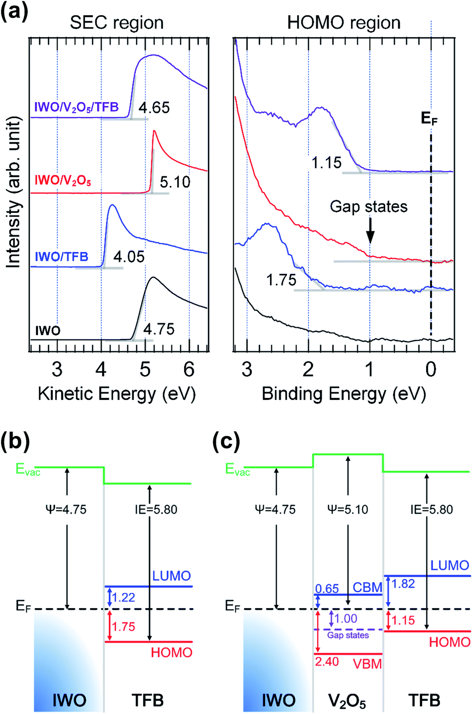 | ||
| Fig. 1 (Color online) (a) measured UPS spectra of the IWO, IWO/TFB, IWO/V2O5, and IWO/V2O5/TFB at the SEC and HOMO region. Interfacial energy level diagram of (b) IWO/TFB and (c) IWO/V2O5/TFB. | ||
The HOD has been fabricated to evaluate the hole injection and transport process from the IWO into the TFB through the V2O5 inserting layer. As shown in the inset of Fig. 2, the structure of the HOD is composed of IWO/V2O5/TFB/Al layers. In this configuration, holes can easily flow from the IWO to Al electrodes, while electrons have difficulty flowing from Al to the IWO electrodes due to the high electron injection barrier. Therefore, the HOD is useful to evaluate the hole injection and transport behavior. Fig. 2 shows the current density–voltage (J–V) characteristics of the HOD. The slope of the J–V curve was calculated as ∼1.5 at the low voltage region, which indicates that the ohmic conduction (J ∝ V) is dominant. The slope changed to ∼2.2 when the voltage exceeded 3 V, which indicates that the space charge limited conduction (SCLC, J ∝ V2) is dominant. Consistent with the interfacial energy level diagram of Fig. 1(c), holes can efficiently inject from the IWO into TFB through V2O5. Moreover, the measured hole mobility was 27.8 cm2 V−1 s−1, which is high enough for the HIL layer. Therefore, the gap states of V2O5 play a key role in injecting hole carriers into the device.
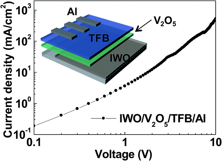 | ||
| Fig. 2 (Color online) voltage–current density characteristic of the IWO/V2O5/TFB/Al HOD. The inset shows the schematic of the HOD. | ||
Fig. 3(a) shows the schematic of the QLEDs with the IWO transparent electrode and V2O5 HIL. The IWO layer was sputtered on a glass substrate, and V2O5, TFB, QDs, and ZnO layers were spin-coated on the IWO surface. Then Al was deposited using a thermal evaporator with a shadow mask. Fig. 3(b) shows the energy level diagram of the QLEDs. All energy levels were aligned according to the EF. Holes can inject from the IWO into QDs through the gap states of V2O5, and HOMO of the TFB. Although there is a possibility of charge generation effect by moving electrons from the HOMO of the TFB into the conduction band minimum (CBM) of V2O5, it hardly occurs due to the high barrier from the HOMO of TFB to the CBM of V2O5 (1.8 eV).27 Fig. 3(c) shows the cross-sectional HRTEM images of the QLEDs. Clearly, all IWO, V2O5, TFB, QDs, ZnO, and Al layers were uniformly coated and well defined, as shown in the image. The inset shows the Fast Fourier Transform (FFT) of the IWO film, which clearly indicated the crystalline structure of the IWO film with the (222) preferred orientation even though it was prepared at room temperature. Fig. 4(a) shows the normalized electroluminescence (EL) spectrum of the QLEDs with the IWO anode and V2O5 HIL. The emission peak of the spectrum was located at 536 nm, and the full-width at half maximum was measured as 30.5 nm. The inset shows a photographic image of the turned-on QLEDs. Fig. 4(b) shows the luminance and current density as a function of applied voltage. The maximum luminance was measured as 9443.5 cd m−2 at the applied voltage of 7.6 V. The turned-on voltage was 2.6 V. The maximum luminance of QLEDs with ITO/PEDOT:PSS/TFB structure showed the maximum luminance of 9710.6 cd m−2 and turn-on voltage of 3.5 V. The current density of QLEDs expressed the behavior of hole and electron current through the device. Fig. 4(c) shows the current density vs. voltage in a log scale of each axis. Under the voltage of 2.2 V, the slope of J–V was ∼1.5, which indicates that the ohmic conduction was dominant. The slope was changed to ∼4.2 at the applied voltages between 2.2 and 4.6 V. In this range, the trap limited SCLC (J ∝ Vn, n > 2) was dominant. Above the voltage of 4.6 V, the slope approached ∼2.1, which shows the SCLC (J ∝ V2) behavior is dominant. The inset shows the life-time characteristics of the QLEDs with IWO/V2O5. The initial luminance was 1000 cd m−2, and the curves were measured under ambient conditions at room temperature. Consistent with the interfacial energy level diagram shown in Fig. 1(c), the QLEDs with the IWO anode and V2O5 HIL worked well due to the hole injection through the gap states of V2O5.
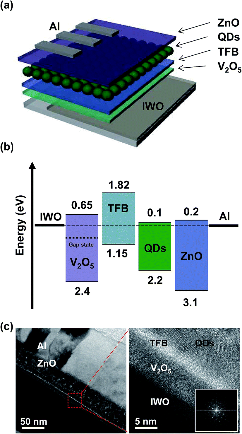 | ||
| Fig. 3 (Color online) (a) schematic of the QLEDs on the IWO transparent electrode. (b) Energy level diagram, aligned to the EF, of the QLEDs. The hole can be injected through the gap state of the V2O5 HIL. (c) Cross-sectional HRTEM images of the QLEDs. The inset shows the FFT pattern of the IWO. | ||
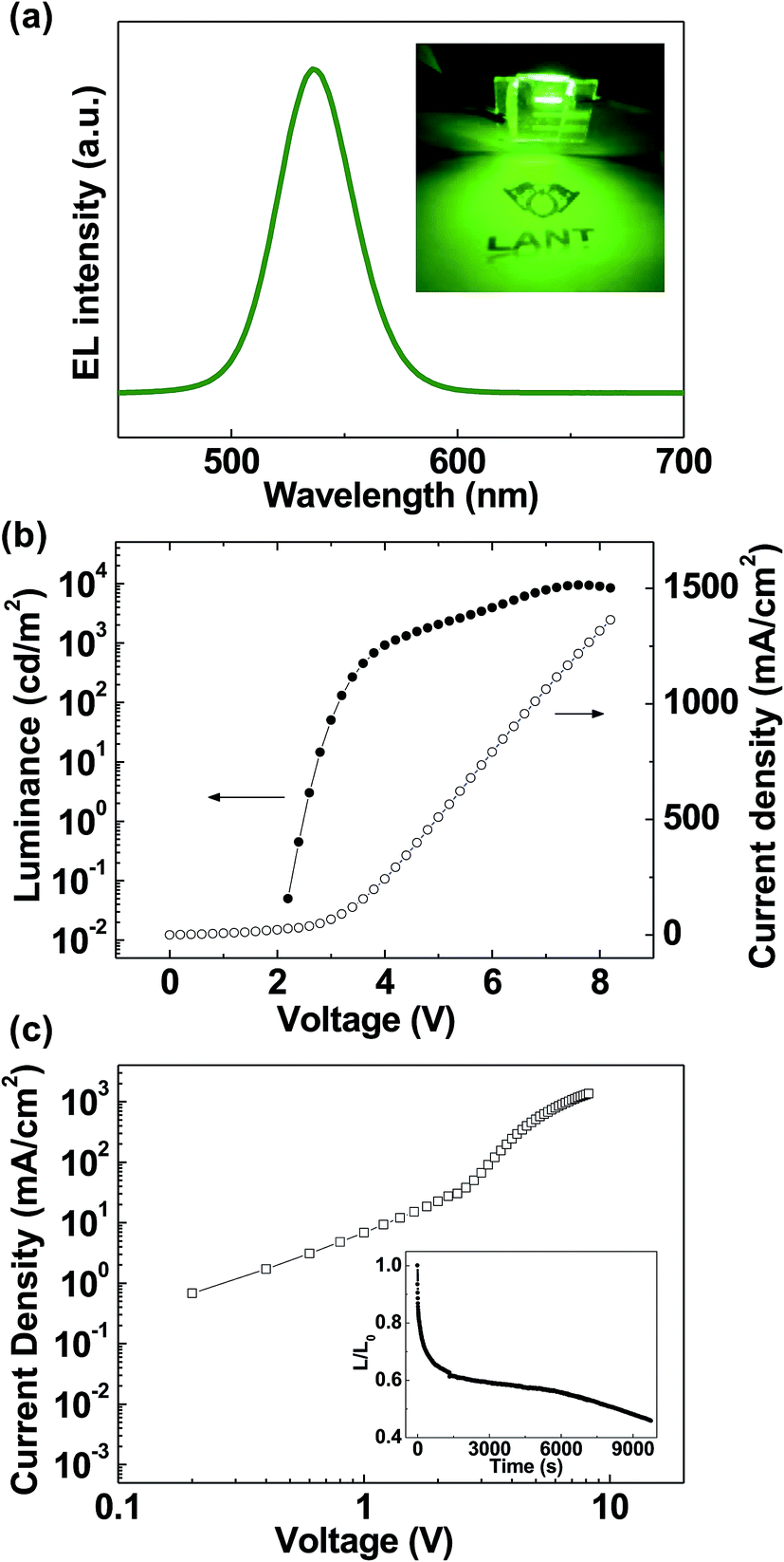 | ||
| Fig. 4 (Color online) (a) EL characteristics of QLEDs on a glass/IWO substrate. The inset shows the turned-on QLEDs. (b) Luminance and current density vs. applied voltage curves. (c) J–V curve in a log-scale. The inset shows the life-time characteristics of the QLEDs. | ||
Conclusion
In conclusion, the hole injection mechanism from the IWO electrode into the TFB through the V2O5 HIL was investigated in detail using UPS. Complete interfacial energy level diagrams of the IWO/TFB and IWO/V2O5/TFB were evaluated from the UPS spectra. We found gap states inside the band gap of V2O5, located at 1.0 eV below the EF. These gap states can provide a hole injection pathway, and the hole injection behavior was confirmed by characterizing the HOD. Conventional-structured QLEDs were successfully fabricated on a glass substrate with the IWO transparent electrode and V2O5 HIL. The maximum luminance of the device was measured as 9443.5 cd m−2. Our result suggests that the IWO electrode and V2O5 HIL are a good combination for developing high-performance and inorganic QLEDs.Conflicts of interest
There are no conflicts to declare.Acknowledgements
This work was supported by a research project grant from the National Research Foundation of Korea (NRF-2016R1D1A1B03932144).References
- J. R. Manders, L. Qian, A. Titov, J. Hyvonen, J. T. Scott, K. P. Acharya, Y. Yang, W. Cao, Y. Zheng, J. Xue and P. H. Holloway, J. Soc. Inf. Disp., 2015, 23, 523 CrossRef CAS.
- B. S. Mashford, M. Stevenson, Z. Popovic, C. Hamilton, Z. Zhou, C. Breen, J. Steckel, V. Bulovic, M. Bawendi, S. C. Sullivan and P. T. Kazlas, Nat. Photonics, 2013, 7, 407 CrossRef CAS.
- H. Shen, Q. Lin, W. Cao, C. Yang, N. T. Shewmon, H. Wang, J. Niu, L. S. Li and J. Xue, Nanoscale, 2017, 9, 13583 RSC.
- X. Yang, E. Mutlugun, C. Dang, K. Dev, Y. Gao, S. T. Tan, X. W. Sun and H. V. Demir, ACS Nano, 2014, 8, 8224 CrossRef CAS PubMed.
- S. Baskoutas and A. F. Terzis, J. Appl. Phys., 2006, 99, 013708 CrossRef.
- K. H. Lee, C. Y. Han, H. D. Kang, H. Ko, C. Lee, J. Lee, N. Myoung, S. Y. Yim and H. Yang, ACS Nano, 2015, 9, 10941 CrossRef CAS.
- J. Kwak, W. K. Bae, D. Lee, I. Park, J. Lim, M. Park, H. Cho, H. Woo, D. Y. Yoon, K. Char, S. Lee and C. Lee, Nano Lett., 2012, 12, 2362 CrossRef CAS PubMed.
- W. K. Bae, J. Lim, D. Lee, M. Park, H. Lee, J. Kwak, K. Char, C. Lee and S. Lee, Adv. Mater., 2014, 26, 6387 CrossRef CAS PubMed.
- J. Meyer, T. Winkler, S. Hamwi, S. Schmale, H. H. Johannes, T. Weimann, P. Hinze, W. Kowlasky and T. Riedl, Adv. Mater., 2008, 20, 3839 CrossRef CAS.
- K. Schulze, B. Maennig, K. Leo, Y. Tomita, C. May, J. Hupkes, E. Brier, D. Reinold and P. Bauerle, Appl. Phys. Lett., 2007, 91, 073521 CrossRef.
- K. Utsumi, O. Matsunaga and T. Takahata, Thin Solid Films, 1998, 334, 30 CrossRef CAS.
- W. Deng, T. Ohgi, H. Nejo and D. Fujita, Appl. Phys. A, 2001, 72, 595 CrossRef CAS.
- X. Dai, Z. Zhang, Y. Jin, Y. Niu, H. Cao, X. Liang, L. Chen, J. Wang and X. Peng, Nature, 2014, 515, 96 CrossRef CAS PubMed.
- X. Yang, E. Mutlugun, Y. Zhao, Y. Gao, K. S. Leck, Y. Ma, L. Ke, S. T. Tan, H. V. Demir and X. W. Sun, Small, 2013, 10, 247 CrossRef.
- X. Jiang, F. L. Wong, M. K. Fung and S. T. Lee, Appl. Phys. Lett., 2003, 83, 1875 CrossRef CAS.
- J. A. Jeong, Y. J. Jeon, S. S. Kim, B. K. Kim, K. B. Chung and H. K. Kim, Sol. Energy Mater. Sol. Cells, 2014, 122, 241 CrossRef CAS.
- Z. Lu, F. Meng, Y. Cui, J. Shi, Z. Feng and Z. Liu, J. Phys. D: Appl. Phys., 2013, 46, 075103 CrossRef.
- J. Kim, J. Lee, S. M. Jo, B. D. Chin, J. Baek, K. Ahn, S. J. Kang and H. Kim, Sci. Rep., 2018, 8, 12019 CrossRef.
- F. Meng, J. Shi, Z. Liu, Y. Cui, Z. Lu and Z. Feng, Sol. Energy Mater. Sol. Cells, 2014, 122, 70 CrossRef CAS.
- S. M. Lee, D. Shin, N. K. Cho, Y. Yi and S. J. Kang, Curr. Appl. Phys., 2017, 17, 442 CrossRef.
- C. Zheng, F. Li, Q. Zeng, H. Hu and T. Guo, Thin Solid Films, 2019, 669, 387 CrossRef CAS.
- Y. Zhang, S. Wang, L. Chen, Y. Fang, H. Shen and Z. Du, Org. Electron., 2017, 44, 189 CrossRef CAS.
- T. Ding, X. Yang, L. Bai, Y. Zhao, K. E. Fong, N. Wang, H. V. Demir and X. W. Sun, Org. Electron., 2015, 26, 245 CrossRef CAS.
- H. T. Nguyen, N. D. Nguyen and S. Lee, Nanotechnology, 2013, 24, 115201 CrossRef PubMed.
- B. A. Bhat, G. R. Khan and K. Asokan, RSC Adv., 2015, 5, 52602 RSC.
- J.-H. Kim, H.-J. Seok, H.-J. Seo, T.-Y. Seong, J. H Heo, S.-H. Lim, K.-J. Ahn and H.-K. Kim, Nanoscale, 2018, 10, 20587 RSC.
- J. Meyer, K. Zilberberg, T. Riedl and A. Kahn, J. Appl. Phys., 2011, 110, 033710 CrossRef.
| This journal is © The Royal Society of Chemistry 2019 |