 Open Access Article
Low-voltage self-assembled indium tin oxide thin-film transistors gated by microporous SiO2 treated by H3PO4
Wei
Dou
 *a and
Yuanyuan
Tan
b
aKey Laboratory of Low Dimensional Quantum Structures and Quantum Control, Hunan Normal University, Changsha 410081, People's Republic of China. E-mail: douwei139@163.com
bHunan First Normal University, Changsha, 410205, People's Republic of China
First published on 27th September 2019
Abstract
Ultralow-voltage (0.8 V) thin-film transistors (TFTs) using self-assembled indium-tin-oxide (ITO) as the semiconducting layer and microporous SiO2 immersed in 5% H3PO4 for 30 minutes with huge electric-double-layer (EDL) capacitance as the gate dielectric are fabricated at room temperature. The huge EDL specific capacitance is 8.2 μF cm−2 at 20 Hz, and about 0.7 μF cm−2 even at 1 MHz. Both enhancement mode (Vth = 0.15 V) and depletion mode (Vth = −0.26 V) operation are realized by controlling the thickness of the self-assembled ITO semiconducting layer. Electrical characteristics with the equivalent field-effect mobility of 65.4 cm2 V−1 s−1, current on/off ratio of 2 × 10⁶, and subthreshold swing of 80 mV per decade are demonstrated, which are promising for fast-switching and low-power electronics on temperature-sensitive substrates.
Introduction
Thin-film transistors gated by traditional SiO2 with high capacitance materials enable lower operating voltages, reduced power consumption and improved performance.1,2 Several strategies have been developed, including reducing dielectric thickness and using high-k dielectrics, to achieve large capacitances.3,4 Herein, an intriguing solution-processed approach is reported that the microporous SiO2 dielectric is immersed into 5% H3PO4, which can dramatically improve the capacitance Ci of the microporous SiO2. The solution-based technique is an attractive candidate for low-cost but high-performance TFTs, because of process simplicity, low cost and chemical composition/stoichiometry control.5,6 The solution process can reduce the cost of electronic devices in existing applications and meet increasing demands to incorporate electronics in new applications. The room-temperature conditions enable the solution-based technique to be suitable for a wide range of substrate materials, which opens opportunities to fabricate electronics on plastic substrates for flexible applications.7Therefore, both depletion and enhancement mode operation are realized by controlling the thickness of the self-assembled ITO semiconducting layer. When the depletion mode and enhancement mode TFTs are employed in circuits, the signal integrity is higher, power consumption is lower and circuit design is simple, so both operation mode TFTs are required for circuit applications.8,9 Up to now, ultralow-voltage oxide-based TFTs with controllable operation mode are rarely reported. In this paper, transparent ITO-TFTs gated by microporous SiO2 immersed into 5% H3PO4 for 30 minutes are fabricated at room temperature, both depletion and enhancement mode operation are realized by controlling the thickness of the self-assembled ITO semiconducting layer. The EDL operating mechanism of solution-processed microporous SiO2 and electrical characteristics of ITO-TFTs are studied. The combination of ultralow-voltage, controlled operation modes and room-temperature processing makes the as-fabricated TFTs attractive for low-power, large-area, and flexible applications, such as low-cost logic, identification tags, smartcards and many form factors incorporating displays.
Experimental
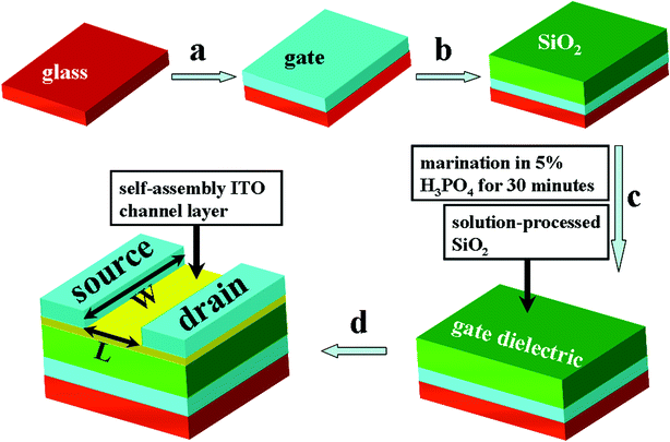
The entire process of transparent ITO-TFTs fabrication was performed at room temperature, as shown in Fig. 1. First, 200 nm-thick ITO gate electrode was deposited on glass substrate by radio frequency (RF) magnetron sputtering. Then, microporous SiO2 gate dielectric with the thickness of 2.5 μm was deposited by plasma-enhanced chemical vapor deposition (PECVD) method. Next, the samples were immersed into 5% H3PO4, which was processed at room temperature. After 30 minutes, these samples were taken out and dried in laundry drier. Finally, ITO source and drain electrodes were deposited by dc sputtering and patterned using a nickel shadow mask, at the same time, self-assembled ITO semiconducting layer was patterned to be the channel layer with a channel length of 80 μm and a channel width of 1000 μm in pure argon ambient at 0.5 Pa. With the thickness of the self-assembled channel layer is from 10 nm to 40 nm, the field-effect mobility μFE increased from 22.5 to 65.4 cm2 V−1 s−1, the threshold voltage Vth decreased from 0.15 V to −0.26 V, and the subthreshold voltage swing S decreased from 100 mV per decade to 80 mV per decade. The electrical transport measurements of ITO transparent TFTs were recorded with a semiconductor parameter characterization system (Keithley 4200 SCS) and a micromanipulator probe station in a clean and shielded box at room temperature in air. The optical transmittance was measured using a spectrophotometer in the wavelength range from 200 to 1000 nm. The capacitance of the microporous SiO2 immersed into 5% H3PO4 for 30 minutes was characterized by the capacitance–frequency (C–f) measurement using an Agilent 4294A precision impedance analyzer. | ||
| Fig. 1 Fabrication of self-assembly ITO TFTs gated by solution-processed microporous SiO2 on glass substrates. | ||
Results and discussion
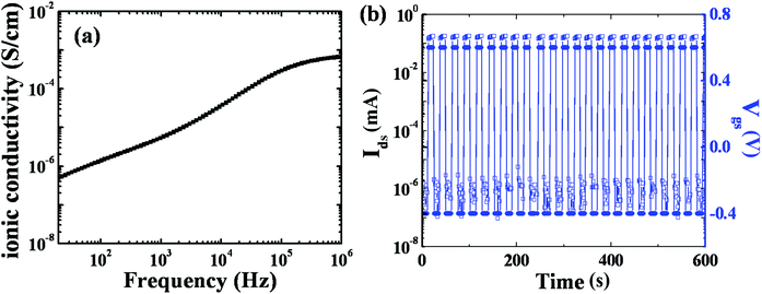
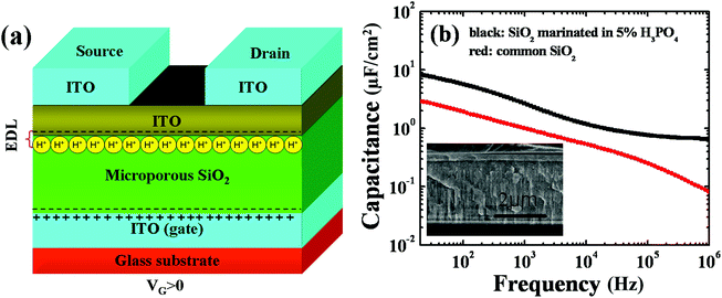
The ultralow voltage operation mechanism of the ITO-TFTs gated by the solution-processed microporous SiO2 is shown in Fig. 2(a). On account of immersing into 5% H3PO4 for 30 minutes, some protons enter the microporous SiO2 and some anions adhere to the surface of the microporous SiO2, these anions induce image charges of equal density and opposite sign in the dielectric layer, which is similar to the case of EDL organic transistors gated by ionic liquids or solid state electrolytes.10,11 The major advantage of the EDL effect is that the specific capacitance is exceptionally large which results in an ultrahigh current throughput at an ultralow operating voltage of 0.8 V. Its transformation may be driven by proton transfer to and from a water molecule with very little permittivity temperature dependence.12–15 To further support the formation of EDL at microporous SiO2/ITO channel interface, Fig. 2(b) depicts the capacitance–frequency curves in wide range frequency from 20 Hz to 1 MHz. The solution-processed microporous SiO2 shows a huge specific capacitance of 8.2 μF cm−2 at 20 Hz and the common SiO2 has a capacitance of 2.8 μF cm−2 with the same thickness of 2.5 μm by the inset. As shown in the picture, both capacitance values of the SiO2 dielectrics decrease with increasing frequency. In particular, the common SiO2 showed a stronger dependence on frequency than the solution-processed microporous SiO2, and the specific capacitance of the solution-processed microporous SiO2 still reach a value of 0.7 μF cm−2 even at 1 MHz, which suggest that the polarization response time of the solution-processed microporous SiO2 is scarcely limited by the ion mobilities and the operation of these TFTs gated by such dielectric at this frequency should be possible. However, the potential switching speed of such TFTs is not solely determined by the capacitance–frequency characteristic; it also depends on the conductivity–frequency response as discussed below.16Fig. 3(a) displays a log–log plot of the frequency dependence of ionic conductivity for the solution-processed microporous SiO2. The lower ionic conductivity of microporous SiO2 at low frequency is due to interfacial impedance (capacitance). According to the value of the ionic conductivity, there are two different frequency regions. At lower frequencies (f < 150 Hz), most of the ionic species accumulate near the electrode/microporous SiO2 interfaces, leading to a cancellation of the electric field in the bulk and, thus, an apparent drop in ionic conductivity. This capacitive behaviour is associated with the formation of an EDL at the ITO/microporous SiO2 interfaces. At higher frequencies (f > 150 Hz), the ionic conductivity of H3PO4-immersed SiO2 increases with frequencies. This capacitive behaviour is considered to be resulted from the dipolar relaxation of the H3PO4-immersed SiO2 dielectric. The impedance spectroscopy of H3PO4-immersed SiO2 dielectric is similar to the typical solid electrolytes and ion gels, indicating that it is an electronically insulating, ionically conducting dielectric.17,18 The drain current response to a square wave pulse gate voltage is shown in Fig. 3(b), ITO-TFTs gated by solution-processed microporous SiO2 were continuously cycled between on and off states (period square wave pulses of Vgs = +0.6 V to −0.4 V and Vds = 0.6 V), these devices maintained current on/off ratios of 105 and without decrease in on current at 0.05 Hz, which strongly suggests the low-voltage operation of ITO-TFTs gated by microporous SiO2 immersed into 5% H3PO4 for 30 minutes.
 | ||
| Fig. 3 (a) Frequency dependence of the ionic conductivity for the solution-processed microporous SiO2. (b) The drain current response to a square wave pulse gate voltage for 0.05 Hz. | ||
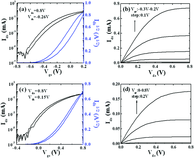
The operation mode of TFTs can be classified as depletion mode and enhancement mode in terms of the polarity of the threshold voltages. The electrical characteristics of ITO-TFTs based on self-assembled ITO semiconducting layer are summarized in Fig. 4. Fig. 4(a) and (c) show the transfer curves displayed in logarithmic scale and (Ids)1/2–Vgs in dual gate sweep mode of the TFTs with 40 and 10 nm ITO channels, respectively. The transfer characteristics (Ids)1/2–Vg curve in Fig. 4(a) shows that a threshold voltage (Vth) of −0.26 V, indicating depletion mode behavior, and the Ids–Vgs curve shows good current on/off ratio of 2 × 10⁶, subthreshold voltage swing (S) of 80 mV per decade and high field effect mobility (μFE) of 65.4 cm2 V−1 s−1 calculated by Ids = (WCi/2L) μFE(Vgs–Vth)2, where, Ci is the specific capacitance (8.2 μF cm−2 at 20 Hz) of microporous SiO2 immersed into 5% H3PO4 for 30 minutes, L is the channel length of 80 μm, W is the channel width of 1000 μm, Vds = 0.8 V, Vth = −0.26 V, and Ids = 0.71 mA at Vgs = 0.2 V. However, in Fig. 4(c), with the thickness of the self-assembled ITO channel decreased from 40 nm to 10 nm, the field effect mobility (μFE) decreased from 65.4 cm2 V−1 s−1 to 22.5 cm2 V−1 s−1, the subthreshold voltage swing (S) increased from 80 mV per decade to 100 mV per decade, the current on/off ratio increased from 2 × 10⁶ to 2 × 10⁷, the threshold voltage (Vth) increased from −0.26 V to 0.15 V, so the TFT with 10 nm self-assembled ITO channel operate in enhancement mode. The large mobilities of both enhancement mode (Vth = 0.15 V) and depletion mode (Vth = −0.26 V) TFTs probably derive from the high charge density in the channel, because the carrier mobility in polymer semiconductors is strongly dependent on carrier density, which result in increased trap filling and a general smoothing of electrostatic potential variations in the film due to trapped charge, these combined effects lead to higher carrier mobilities.19,20Fig. 4(b) and (d) show source-drain current (Ids) versus source-drain voltage (Vds) curves of the TFTs with 40 and 10 nm ITO channels, respectively. In Fig. 4(b), the gate-source voltage (Vgs) is increased from −0.3 V to 0.2 V in steps of 0.1 V, and in Fig. 4(d)Vgs from 0 to 0.8 V in steps of 0.2 V. Both devices exhibited nice pinch-off, high on-current and hard saturation characteristics with steep rise in the low drain-source voltage (Vds), which indicates that the microporous SiO2 immersed into 5% H3PO4 for 30 minutes is very promising for practical applications of transistor.
 | ||
| Fig. 4 (a) The transfer curves and (b) output characteristics of the TFTs with 40 nm ITO channel. (c) The transfer curves and (d) output characteristics of the TFTs with 10 nm ITO channel. | ||
Conclusions
In conclusion, ultralow-voltage transparent ITO-TFTs with EDL effect are fabricated at room temperature. Such devices gated by microporous SiO2 immersed into 5% H3PO4 for 30 minutes exhibit high current output and ultralow-voltage (0.8 V) operation, the huge EDL specific capacitance is 8.2 μF cm−2 at 20 Hz and ∼0.7 μF cm−2 at 1 MHz. Both enhancement mode (Vth = 0.15 V) and depletion mode (Vth = −0.26 V) operation are realized by controlling the thickness of the self-assembled ITO semiconducting layer. The combination of low operating voltage (0.8 V), high field effect mobility (22.5–65.4 cm2 V−1 s−1), high current on/off ratio (2 × 10⁶ to 2 × 10⁷), steep subthreshold swing (80–100 mV per decade) and room temperature processing make the transparent ITO-TFTs very promising for fast-switching and low-power electronics on temperature-sensitive substrates.Conflicts of interest
There are no conflicts to declare.Notes and references
- J. C Lee, M. J. Panzer, Y. He, T. P. Lodge and C. D. Frisbie, J. Am. Chem. Soc., 2007, 129, 4532 CrossRef.
- S. Y. Yang, S. H. Kim, K. Shin, H. Jeon and C. E. Park, Appl. Phys. Lett., 2006, 88, 173507 CrossRef.
- I. D. Kim, M. H. Lim, K. T. kang, H. G. Kim and S. Y. Choi, Appl. Phys. Lett., 2006, 89, 022905 CrossRef.
- S. H. Hur, M. H. Yoon, A. Gaur, M. Shim, A. Fachetti, T. J. Marks and J. A. Rogers, J. Am. Chem. Soc., 2005, 127, 13808 CrossRef CAS.
- B. S. Ong, C. Li, Y. Li, Y. Wu and R. Loutfy, J. Am. Chem. Soc., 2007, 129, 2750 CrossRef CAS.
- H. S. Kim, P. D. Byrne, A. Facchetti and T. J. Marks, J. Am. Chem. Soc., 2008, 130, 12580 CrossRef CAS.
- C. J. Drury, C. M. J. Mutsaers, C. M. Hart, M. Matters and D. M. de Leeuw, Appl. Phys. Lett., 1998, 73, 108 CrossRef CAS.
- C. A. Lee, S. H. Jin, K. D. Jung, J. D. Lee and B.-G. Park, Solid-State Electron., 2006, 50, 1216 CrossRef CAS.
- R. Wang, Y. Cai, C.-W. Tang, K. M. Lau and K. J. Chen, IEEE Electron Device Lett., 2006, 27, 793 CAS.
- T. Uemura, M. Yamagishi, S. Ono and J. Takeya, Appl. Phys. Lett., 2009, 95, 103301 CrossRef.
- B. N. Pal, B. M. Dhar, K. C. See and H. E. Katz, Nat. Mater., 2009, 8, 898 CrossRef CAS.
- Y. F. Chang, B. Fowler, Y. C. Chen, Y. T. Chen, Y. Wang, F. Xue, F. Zhou and J. C. Lee, J. Appl. Phys., 2014, 116, 043708 CrossRef.
- Y. F. Chang, B. Fowler, Y. C. Chen, Y. T. Chen, Y. Wang, F. Xue, F. Zhou and J. C. Lee, J. Appl. Phys., 2014, 116, 043709 CrossRef.
- E. Terzini, P. Thilakan and C. Minarini, Mater. Sci. Eng., B, 2000, 77, 110 CrossRef.
- Y. Wang, B. Fowler, F. Zhou, Y. F. Chang, Y. T. Chen, F. Xue and J. C. Lee, Appl. Phys. Lett., 2013, 103, 213505 CrossRef.
- J. Lee, L. G. Kaake, J. H. Cho, X.-Y. Zhu, T. P. Lodge and C. D. Frisbie, J. Phys. Chem. C, 2009, 113, 8972 CrossRef CAS.
- M. Venkateswarlu and N. Satyanarayana, Mater. Sci. Eng., B, 1998, 54, 189 CrossRef.
- N. Bagdassarov, H.-C. Freiheit and A. Putnis, Solid State Ionics, 2001, 143, 285 CrossRef CAS.
- M. C. J. M. Vissenberg and M. Matters, Phys. Rev. B: Condens. Matter Mater. Phys., 1998, 57, 12964 CrossRef CAS.
- C. Tanase, E. J. Meijer, P. W. M. Blom and D. M. de Leeuw, Phys. Rev. Lett., 2003, 91, 216601 CrossRef CAS.
| This journal is © The Royal Society of Chemistry 2019 |

