Harnessing MOF materials in photovoltaic devices: recent advances, challenges, and perspectives
Chu-Chen
Chueh
 *ab,
Chih-I
Chen
ab,
Yu-An
Su
ab,
Hannelore
Konnerth
a,
Yu-Juan
Gu
c,
Chung-Wei
Kung
 *c and
Kevin C.-W.
Wu
 *ade
*ade
aDepartment of Chemical Engineering, National Taiwan University, No. 1, Sec. 4, Roosevelt Road, Taipei 10617, Taiwan. E-mail: cchueh@ntu.edu.tw
bAdvanced Research Center for Green Materials Science and Technology, National Taiwan University, Taiwan
cDepartment of Chemical Engineering, National Cheng Kung University, No. 1, University Road, Tainan City 701, Taiwan. E-mail: cwkung@mail.ncku.edu.tw
dCenter of Atomic Initiative for New Materials (AI-MAT), National Taiwan University, Taiwan
eInternational Graduate Program of Molecular Science and Technology (NTU-MST), National Taiwan University, Taiwan. E-mail: kevinwu@ntu.edu.tw
First published on 29th April 2019
Abstract
Metal–organic framework (MOF) materials have achieved significant research interest in the fields of gas storage and separation over the last two decades because of the need for hydrogen utilization and carbon dioxide reduction. Besides, recently numerous functional MOFs have been exploited and applied in the optoelectronic field owing to some unique properties of MOF materials in those photovoltaic devices with enhanced performance and stability. This review focuses on the comprehensive summary of recent representative progress in the applications of MOFs in solar cell devices, including dye-sensitized solar cells, organic–inorganic hybrid perovskite solar cells, and organic solar cells, aiming to portray their prospects in the future.
1. Introduction to MOFs
Metal–organic frameworks (MOFs) are defined as coordination compounds which consist of polynuclear metal nodes and organic linkers building a crystalline open framework structure.1–3 Their properties include a high specific surface area (up to 7000 m2 g−1 (ref. 4 and 5)) and high porosity. MOFs are a relatively new class of compounds, whose development started at the beginning of 1990 by the pioneering studies of Robson,6,7 Yaghi,8 Kitagawa,9 and Férey,10 and the term MOF was introduced only in 1995 by Yaghi.8 Later gas sorption measurements demonstrated for the first time the porosity of these materials and the determination of their surface area, as well as the pore volume, which allows for a fair comparison with other porous materials.9,11 The key development of these porous materials was marked by the introduction of secondary building units (SBUs). The polynuclear properties result in the formation of extended porous networks and thus the synthesis of stable and rigid structures.12 In the next two decades, the number of scientific research articles and patented literature pertaining to MOF synthesis and application has increased tremendously.Generally, the synthesis of MOFs is based on a self-assembly approach of a metal-precursor and organic linkers, and is conventionally carried out under hydro- or solvothermal conditions; however, mechanochemical, electrochemical or ultrasonic, and microwave irradiation procedures are also widely used nowadays.13 With the development of stable MOFs by choosing appropriate metal ions and ligands to strengthen the coordinative bonds in the frameworks, it is possible to improve the hydrothermal stability significantly,14,15 enabling the widespread applications of MOF materials. The diverse capabilities of MOFs are based on a variety of combinations of metal nodes and organic linkers. This flexibility in the synthesis of MOFs enables the facile tuning of their morphological properties like surface area and porosity, thus realizing a target-oriented synthesis and applicability.
MOFs and MOF-derived materials have been utilized in various fields such as energy-related applications and catalysis like electrocatalysis, photocatalysis, and biocatalysis in recent years.16–20 The use of MOFs is especially focused on gas storage,21–23 sensors,24,25 techniques for separation and purification,26,27 and catalysis.28,29 The desired properties of MOFs for specific applications as well as the catalytic activity can either arise from the coordinative unsaturated metal centre or functional groups attached to the framework. Post-synthetic methods further facilitate modification and expansion of MOF functionalities.30,31
MOFs can also serve as a platform for guest compounds which can be embedded in or attached to the framework such as metal complexes, metal nanoparticles (NPs) or even biomolecules like enzymes.32–37 In these cases, the MOF acts as the support affording high stability and porosity to provide a scaffold with confined spaces resulting in size-selective catalysis.13,38–40 Moreover, the design of MOF hybrid materials with polymers or ionic liquids is of considerable interest to further explore and enhance the stability and functionality of MOF materials in diverse research fields.41–43
On the other hand, MOF-derived materials like porous carbon, metals, metal oxides, metal sulphides and metal phosphides as well as hybrid materials become increasingly attractive due to the diversity in tuning the derived material by careful adjustment of the MOF precursor, guest species and synthesis conditions.18–20,44–47 In the field of MOF-derived materials, both Wu's group and Yamauchi's group have contributed considerably. They developed a simple, direct route from MOFs to highly functional nanoporous carbon without the need of organic additives acting as the carbon source.48 MOF-derived materials can be prepared by calcination or pyrolysis of MOFs, in which the annealing temperature and time, heating rate, gas atmosphere (air or inert) and the MOF precursor itself determine the resulting structure and chemical composition of the material. For example, heteroatom-doping of carbon materials can be achieved by choosing the appropriate precursor materials. Furthermore, MOFs with guest species like metal NPs can be converted into materials with a desired composition and high dispersion of the active metal on the derived MOF support. Characterized by their high surface area and porosity due to the inherited MOF structure for the most part, as well as enhanced stability, MOF-derived materials become desirable candidates for various catalytic applications.18 Thus scientific research on MOF and MOF-derived porous materials with high structural variability is desirable for the further development in different areas such as energy-related processes. Recently, with the rapid development of photovoltaic techniques, harnessing MOF materials in energy applications is continuously increasing and seems to start growing. Herein, we comprehensively summarize some recent representative progress in the applications of MOFs in solar cells, aiming to provide future prospects for both MOF and photovoltaic communities.
2. Photovoltaic application of MOFs
Since the principle of photovoltaic devices is transducing optical signals into electronic circuits, the most straightforward strategy to utilize MOFs in photovoltaic applications is using them as the photoactive materials. Generally, a photovoltaic cell consists of charge-collecting electrodes, charge-transporting layers (CTLs), and the photoactive material, and the photoactive material is sandwiched between the respective CTL and electrodes. When the photoactive materials absorb solar radiation, photoexcitons are sequentially generated, followed by dissociation into free carriers enabled by the built-in voltage in the device and collected by the respective electrodes. In principle, the resulting power conversion efficiency (PCE) is correlated to three parameters: the open-circuit voltage (Voc), short-circuit current density (Jsc), and fill factor (FF) according to the equation PCE = Voc × Jsc × FF/Pinput.To this end, the MOFs should possess decent light-harvesting capability in the region from visible light to near-infrared (NIR) because most of the photons incident on the earth surface were contributed from this region.
As introduced earlier, the structure of MOFs is mainly composed of metal ions and an organic linker, forming a harmonious framework. Given that the electronic configuration of MOFs is contributed by both the constituent metal ion and the organic linker, the resultant bandgap (Eg) and semiconducting properties of MOFs can thus be tailored by their composition engineering. Basically, the material's light-harvesting window is primarily determined by its Eg. Therefore, synthesizing a MOF with a suitable Eg that can absorb light in the solar spectrum is a prerequisite for it to serve as the photoactive material.
Owing to the full shell of the metal ion and low conjugation of the organic linker, MOFs usually possess a relatively large Eg that cannot effectively absorb light in the solar spectrum. For example, isoreticular MOFs (IRMOFs), consisting of Zn2+ ions with a full d shell which were coordinated with aromatic carboxylate linkers, generally possess large Egs, which makes them only absorb UV radiation. It is interesting to note that first principles calculations have recently unveiled that the ligand center of MOFs plays a dominant role in its resulting light-harvesting behavior.49,50 Meanwhile, some experimental results have also shown the charge transfer via the metal–linker interaction.51,52 All these findings suggest that it is feasible to fulfill the photoactive functions of MOFs through rational composition engineering.
Based on this principle, several series of MOFs with suitable Egs and proper light-harvesting capability have been recently exploited. For instance, using metal ions with an open d shell, such as Co2+, Ni2+, and Cu2+ ions,53–55 to substitute the full shell metal ions has been demonstrated as an effective approach to reduce the resulting Egs of derived MOFs, whereas using closed-shell metal ions, like Cd or Mg, only results in subtle changes.56
In the meantime, various simulation techniques have also been applied to explore the effective ways to reduce the Egs of MOFs. Because the simulation can depict the electronic structures for both organic linkers and metallic nodes, it could provide practical guidelines for synthesizing small Eg MOFs. Thus far, the most prevalent simulation method reported for studying the periodic structure of MOFs is based on density functional theory (DFT), which can predict the resultant frontier energy levels, such as the highest occupied molecular orbital (HOMO) and the lowest unoccupied molecular orbital (LUMO). For example, the simulation of Metal–Organic Framework Ulm University-4 (MFU-4)-type MOFs has been recently carried out to understand the Eg relationship with their constituent metal ions and organic linkers.57 Based on the simulation results, Volkmer et al. proposed three approaches to engineer the Eg of MOFs. First, the Eg can be effectively reduced if a metal node that possesses an unoccupied d-orbital below the LUMO level of the organic linker is employed at the octahedral coordination site. Second, increasing the conjugation of the organic linkers can afford a higher-lying HOMO level resulting in a decreased Eg. Third, functionalizing the organic linkers with various electron-donating groups (–NH2, –OH, –CH3, or –Cl) can help to reduce the resultant Eg because they might contribute 2p electrons to the aromatic linker.58
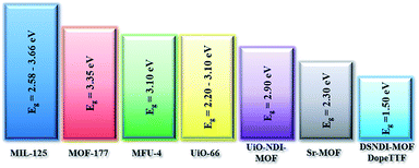
Illustrated in Fig. 1 is the Eg comparison of the collected MOFs comprising various metal ions and organic/conjugated-based linkers while their detailed structures are summarized in Table 1. From this comparison, the approaches proposed by Volkmer et al. to reduce the Eg of MOFs can be clearly clarified.
| Sample | Metal | Linker | E g (eV) | Ref. | |
|---|---|---|---|---|---|
| MIL-125 | Ti |
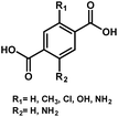
|
BDC-H | 3.68 | 58 |
| BDC-CH3/Cl | 3.50 | ||||
| BDC-OH | 2.80 | ||||
| BDC-NH2 | 2.40 | ||||
| BDC-(NH2)2 | 1.28 | ||||
| MOF-177 | Zn |
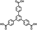
|
BTB | 3.35 | 60 |
| MFU-4 | Zn |

|
BBTA | 3.10 | 57 |
| UiO-66 | Zr |

|
BDC-H | 3.10 | 59 |
| BDC-NO2 | 2.80 | ||||
| BDC-NH2 | 2.20 | ||||
| UiO-NDI MOF | Zr |

|
NDI | 2.90 | 61 |
| Sr-based MOF | Sr |

|
Htbc | 2.30 | 63 |
| DSNDI-based MOF-74 | Zn |

|
DSNDI | 2.50 | 62 |

|
DSNDI doped TTF | 1.50 | |||
As seen, the Egs of MIL-125 MOFs can be effectively modulated by using different side-chain modified benzenedicarboxylate (BDC) linkers. The Eg was reduced from 3.68 eV to 1.28 eV as the side-chain of BDC was replaced with electron-donating amine groups [BDC-(NH2)2].58 Similarly, the Egs of Zr-UiO-66 MOFs were effectively reduced from 3.10 eV to 2.20 eV as the BDC linker was functionalized with electron-donating groups (–NO2 and –NH2).59
On the other hand, the influence of the conjugation of organic linkers on the resultant Eg can be studied by comparing MOF-177 and MFU-4. The more enhanced conjugation of the organic linker of MFU-4 than that of MOF-177 resulted in its smaller Eg.57,60 Similarly, upon replacing the BDC-H linker with a naphthalene diimide (NDI) building block in the UiO-66 MOF (Eg: 3.10 eV), the derived UiO-NDI MOF possessed a smaller Eg of 2.90 eV.61 The NDI linker has also been employed by Saha et al. to synthesize a DSNDI-based MOF-74 showing a small Eg of 2.50 eV.62 They further used a conjugated, electron-rich small molecule, tetrathiafulvalene (TTF), to dope the NDI moiety to enable a very small Eg of 1.50 eV.62 Notably, besides the commonly used metal ions like Ti4+, Zn2+, and Zr4+ ions, the Sr(NO3)2 complex has also been selected to react with a 1,2,4-benzenetricarboxylic acid (Hbtc) linker through hydrothermal methods to form a Sr-based MOF with a small Eg of 2.30 eV.63
From the above discussion, it can therefore be concluded that the following three strategies can effectively reduce the Egs of the synthesized MOFs and enrich their semiconducting properties for photovoltaic applications: (i) selecting electron-rich metal nodes and conjugated-based organic molecules, (ii) enhancing the conjugation of the organic linker, and (iii) functionalizing the organic linker with electron-donating groups, such as hydroxyl, nitro, and amino groups, as illustrated in Fig. 2. Meanwhile, facilitating electron delocalization through guest-mediated π-donor/acceptor stacks can also effectively diminish the Egs of the materials.
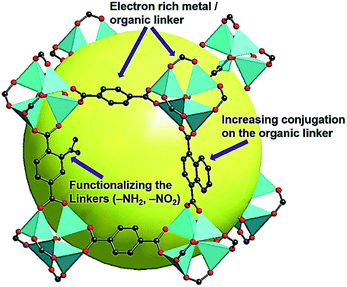 | ||
| Fig. 2 Illustration of the proposed strategies for reducing the Eg of MOFs. Cited from ref. 64. | ||
It is important to note that, besides suitable Egs to cover the solar spectrum, the semiconducting properties of MOFs also play a pivotal role. It is because sufficient dissociation of the photoexcitons generated in the MOFs is required to produce a reasonable photocurrent. In this regard, it imposes critical barriers to use MOFs as the photoactive materials directly and impedes its progress in photovoltaic applications to date. Nevertheless, besides acting as the photoactive materials, the MOFs can still contribute to the photovoltaic community by serving as functional additives or interlayers to improve the performance and stability of the derived solar cell devices. We next will introduce the recent significant progress triggered by MOFs in dye-sensitized solar cells (DSSCs), organic–inorganic hybrid perovskite solar cells (PVSCs), and organic solar cells (OSCs) in the following sections.
3. MOFs in dye-sensitized solar cells (DSSCs)
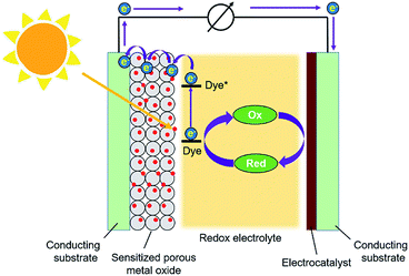
Dye-sensitized solar cells (DSSCs) have attracted considerable attention from researchers all over the world for more than two decades due to their advantages of low cost, easy fabrication, and relatively high efficiency for the conversion of sunlight into electricity.65–67 Generally, a DSSC consists of a photoanode, a counter electrode (CE), and a redox electrolyte, as depicted in Fig. 3. The photoanode is composed of a thin film of a porous semiconducting metal oxide deposited on a conducting and transparent substrate; TiO2 is the most commonly used metal oxide for the photoanode. The metal oxide thin film is sensitized with a photosensitizing dye. Under illumination, the dye molecule absorbs photons from sunlight, which causes electron injection into the conduction band of the semiconducting metal oxide. The electron can flow through the outer circuit towards the CE, as indicated in Fig. 3. The CE consists of a layer of an electrocatalyst deposited on another conducting substrate; a thin film of platinum is usually used as the electrocatalyst. The gap between the photoanode and the CE is filled with an electrolyte solution containing a redox couple; iodide/triiodide (I−/I3−) is the most commonly used redox couple in the electrolyte. By utilizing the electrocatalyst deposited on the CE side, electrochemical reduction of the oxidized form of the redox component, i.e., I3−, happens on the surface of the CE to generate I−. Therefore, the dye molecule in the excited state on the photoanode can be reduced back to its ground state by receiving an electron from I− coming from the electrolyte solution.Due to their interconnected porosity, ultrahigh specific surface area and periodic intra-framework functionality, MOFs have been considered as attractive candidates for electrode materials for a range of electrochemical applications.68 Thus, one can expect that MOF thin films with proper chemical functionalities should also be applicable in DSSCs; the MOF constructed with photosensitizing organic linkers may act as a a promising material for the photoanode in a DSSC to replace the metal oxide, and the MOF that is capable of electrocatalyzing the reduction of I3− may be a potential candidate for the CE to replace the expensive platinum. Although the performance of MOF-based DSSCs may be limited by the electrically insulating nature69,70 and sluggish charge hopping rate71 appearing in most MOFs, MOF-derived materials or MOF-based composite materials can be designed and utilized in DSSCs to improve the cell performance. The early examples of DSSCs with MOFs were reported in 2011,72,73 and utilizing MOFs and relevant materials in DSSCs has become an emerging subfield in recent years.74 In the following section, the recent progress in MOF-based DSSCs is highlighted.
3.1 MOFs as the photoanodes in DSSCs
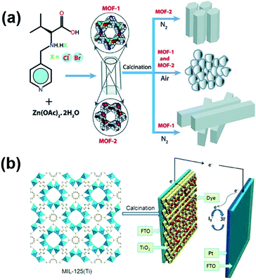
One of the first studies utilizing MOFs in the fabrication of photoanodes in DSSCs was reported by M. Wei et al. in 2011.72 In this study, a thin layer of a zinc-based zeolitic imidazolate framework, ZIF-8, was grown on a TiO2 surface on the photoanode as a blocking layer (Fig. 4a). The ZIF-8 thin film can inhibit the interfacial charge recombination occurring on the TiO2 surface, which results in a significantly increased open-circuit voltage (Voc) than the pristine DSSC without ZIF-8. The dye loading was also found to be much higher in the presence of ZIF-8 on the photoanode. The cell efficiency was enhanced from 5.11% to 5.34% with the help of the ZIF-8 layer at the optimal growth time, but was found to cut back with further increase in the growth time due to the severe decrease in the short-circuit current density (Jsc). In the following study, the same research group also developed an approach to fabricate the ZIF-8/TiO2 photoanode without decreasing the photocurrent.75 A similar strategy was also utilized in DSSCs with a tris(2,20-bipyridine) cobalt(II)/(III)-based electrolyte; with the help of the ZIF-8 layer, the cell efficiency can be enhanced from 7.75% to 9.42%.76 Besides serving as the blocking layer, MOFs constructed with photosensitizing organic linkers may be utilized as the sensitizer for the photoanodes in DSSCs. An early study reported by H. Garcia et al. in 2011 already discovered that a MOF thin film composed of Al2(bdc)3 (bdc: p-benzenedicarboxylate) can be utilized as the photosensitizing material in all-solid-state DSSCs, although the reported photocurrent is still in the order of microampere per square centimeter.73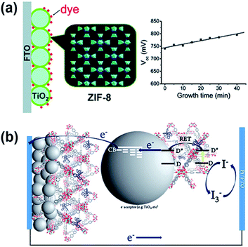 | ||
| Fig. 4 The use of MOFs for the photoanodes in DSSCs as the (a) blocking layer72 and (b) photosensitizer.80 | ||
Several recent studies have shown that a range of MOFs can be utilized as the photosensitizers or co-sensitizers in DSSCs.77–84 For example, S.-H. Han et al. fabricated thin films of a copper-based MOF on the surface of TiO2 thin films using a layer-by-layer (lbl) technique and directly utilized the obtained thin films as the photoanode material in DSSCs. With iodine doping in the MOF, a cell efficiency of 0.26% was achieved, which is much higher than that of the DSSC without the photosensitizing MOF (0.008%).77 The same group also demonstrated the use of ruthenium-based MOF thin films made using the lbl technique as the photosensitizer in DSSCs to achieve a cell efficiency of 1.22%.78 Christof Wöll et al. found that thin films of a porphyrinic MOF grown on conducting substrates can be directly utilized as the photoanodes in DSSCs.79 Similarly, E. D. Spoerke et al. found that the isolated crystals of a porphyrinic MOF can serve as the photosensitizer in DSSCs.81 A. J. Morris et al. also reported the use of a series of highly stable zirconium-based MOFs (UiO-67) incorporating various light-harvesting ruthenium(II) polypyridyl ligands as the photosensitizers in DSSCs (Fig. 4b). Although the resulting efficiency of the DSSC fabricated with the MOF-based light-harvesting sensitizer is still less than 1%, it is much higher than the efficiency of the DSSC fabricated with a monolayer of the same photosensitizing ligand on the surface of TiO2.80 It can be seen that although MOFs can provide a high density of well accessible photosensitizing units, DSSCs fabricated with MOFs as sensitizers still show quite limited cell efficiencies, presumably due to the electrically insulating property of these frameworks.85 Achieving a higher conductivity or a faster charge-transport rate in MOFs becomes the main challenge for utilizing these light-harvesting frameworks in practical photovoltaic devices.
3.2 MOFs as the CEs in DSSCs
The CE is the place where the electrochemical reaction occurs in a DSSC. The CE is not only an essential part of a DSSC, but also a crucial component to determine the cell performance; the electrode material that shows a better electrocatalytic activity for the reduction of triiodide ions can be utilized for CEs to further enhance the overall cell performance. A thin film of platinum is usually used as the CE material, but the design of less expensive electrocatalysts is desirable to reduce the overall cost of DSSCs. In the literature, various electrocatalysts including metal sulfides, metal selenides, metal carbides, metal nitrides, carbons, and conducting polymers, have been utilized in DSSCs as the CE materials.86–88 Due to their periodic intra-framework functionality that enables the formation of high-density and well separated catalytically active sites, MOFs should be potential catalysts for the electrocatalysis occurring on the CE side. However, due to the electrically insulating nature of MOFs, the use of crystalline MOFs as the CEs in DSSCs to electrocatalyze the reduction of triiodide ions is very rare, and the design of composite materials containing MOFs and conducting polymers is usually required to facilitate charge transport in the materials for CEs.89,90 For example, K. C. Ho et al. designed composite materials containing nanocrystals of a porphyrinic zirconium-based MOF (MOF-525) and conducting sulfonated-poly(thiophene-3-[2-(2-methoxyethoxy)-ethoxy]-2,5-diyl) (s-PT) for the CEs in DSSCs (Fig. 5).89 Both s-PT and MOF-525 were found to show electrocatalytic activity toward triiodide ions, and the composite material exhibits a better activity than both the pristine MOF and s-PT. Carbon cloth further served as the underlying substrate for the fabrication of CEs to further facilitate charge transport through the entire CE. As a result, a cell efficiency of 8.91% was achieved by utilizing the CE with the composite material, which is much higher than those of DSSCs fabricated with the CEs consisting of pristine MOF-525 (4.78%), s-PT (6.94%), and conventional platinum (8.21%). A similar design of composite materials for CEs was also reported by X. Zhao et al.90 Composite materials containing ZIF-8 and polystyrenesulfonate-doped poly(3,4-ethylenedioxythiophene) (PEDOT![[thin space (1/6-em)]](https://www.rsc.org/images/entities/char_2009.gif) :
:![[thin space (1/6-em)]](https://www.rsc.org/images/entities/char_2009.gif) PSS) were prepared for the CEs in DSSCs to achieve a cell efficiency of 7.02%, which is much higher than that of the DSSC fabricated with PEDOT
PSS) were prepared for the CEs in DSSCs to achieve a cell efficiency of 7.02%, which is much higher than that of the DSSC fabricated with PEDOT![[thin space (1/6-em)]](https://www.rsc.org/images/entities/char_2009.gif) :
:![[thin space (1/6-em)]](https://www.rsc.org/images/entities/char_2009.gif) PSS-CE (4.00%).
PSS-CE (4.00%).
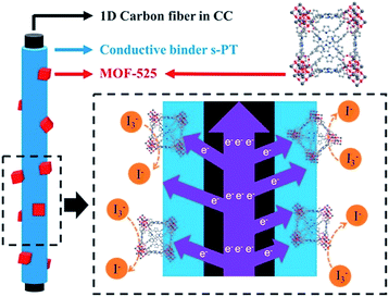 | ||
| Fig. 5 Composite materials containing MOF-525 nanocrystals and conducting s-PT as the CEs in DSSCs.89 | ||
3.3 MOF-derived materials as the photoanodes in DSSCs
As mentioned previously that DSSCs fabricated with MOF-based photosensitizers mostly suffer from a low cell efficiency, presumably attributed to the limited electrical conductivity of the frameworks, another strategy to improve the performance of DSSCs with MOF materials is utilizing MOF-derived metal oxides as the semiconducting dye adsorbent on the photoanode side to replace the conventional metal oxide. As TiO2 and ZnO are the most commonly used semiconducting oxides for photoanodes in DSSCs,91 various metal oxides derived from zinc-based or titanium-based MOFs have been applied for DSSCs as the photoanode materials.92–94 For example, in 2012, R. Banerjee et al. synthesized two zinc-based MOFs and calcined them in air to obtain MOF-derived ZnO crystals (Fig. 6a). The DSSC utilizing MOF-derived ZnO as its photoanode material achieved a cell efficiency of 0.15%, but the DSSCs with MOF-derived ZnO/carbon composites, which were prepared by calcining the MOFs in nitrogen, were found to show negligible cell performance. Similar approaches for converting different zinc-based MOFs into ZnO-based photoanodes for DSSCs were also demonstrated by H. Wang et al. and S. Fujihara et al. to achieve cell efficiencies of 2.52% and 3.37%, respectively.93,94As the DSSCs fabricated with TiO2-based photoanodes generally show better performance compared to the ZnO-based DSSCs, there has also been considerable research effort to design TiO2-based photoanodes derived from titanium-based MOFs.95–97 Since the number of existing Ti-based MOFs so far is still very limited,98 TiO2 synthesized in all of these studies was derived from the most commonly seen Ti-based MOF, MIL-125. In 2015, M. Wei et al. reported the use of hierarchical anatase TiO2 derived from MIL-125 as the photoanodes in DSSCs (Fig. 6b); a cell efficiency of 7.20% was achieved, which is much higher than those of the DSSCs utilizing conventional P25 TiO2 nanoparticles (6.37%).95 L. Yin et al. further incorporated TiO2 derived from MIL-125 with Cu2ZnSnS4 and tin oxide/MoS2 for use as photoanodes in DSSCs and achieved cell efficiencies of 8.10% and 8.96%, respectively.96,97 In addition to serving as the semiconducting dye adsorbent, MOF-derived TiO2 or ZnO can also be utilized as the light scattering layer on the photoanode.99,100 For example, J. H. Kim et al. deposited MOF-derived mesoporous hierarchical TiO2 as the scattering layer onto a nanocrystalline TiO2 layer and utilized the obtained photoanodes in quasi-solid-state DSSCs. The DSSC with the MOF-derived scattering layer achieved an efficiency of 7.1%, which is much higher than that of the DSSC with nanocrystalline TiO2 only (4.6%).99 Moreover, E. Wang et al. reported a strategy to prepare highly dispersed polyoxometalate (POM) nanoparticles composited with TiO2-based photoanodes by the calcination of a POM-based MOF; the resulting DSSC performance can also be enhanced significantly.101
3.4 MOF-derived materials as the CEs in DSSCs
Compared to the pristine MOFs which are usually electrically insulating, MOF-derived materials are more common to be utilized as the CEs in DSSCs. As mentioned previously that metal sulfides, metal selenides, metal nitrides and carbon materials are known platinum-free electrocatalysts to catalyze the reduction of triiodide ions on CEs, one can expect that these materials derived from MOFs should be attractive CE materials for DSSCs. In 2014, our group reported the first example of using MOF-derived materials as the CEs in DSSCs.102 In this study, cobalt sulfide nanoparticles derived from a cobalt-based zeolitic-imidazole framework, ZIF-67, were utilized as the CE material to achieve a cell efficiency of 8.1%, which is comparable to that of the DSSC fabricated with a platinum-based CE (8.0%). Lots of studies utilizing carbon-based materials,103–112 metal sulfides,102,113,114 metal selenides,115,116 and metal carbide117 as the CEs in DSSCs have been reported over the past five years. The cell efficiency (η) of the DSSC fabricated with the MOF-derived CE compared to that of the DSSC with platinum-based CE (Pt-CE) reported in each study mentioned above is summarized in Table 2. Nitrogen-doped carbons derived from MOFs served as the active electrocatalysts or cocatalysts in most examples, and it can be observed that the DSSC fabricated with the MOF-derived CE can achieve a cell efficiency comparable to or higher than that of the cell fabricated with Pt-CE in all of these studies.| MOF-derived CE material | η (%) | η (Pt-CE), (%) | Reference |
|---|---|---|---|
| a Carbon nanotubes. b Nitrogen-doped carbon. c Reduced graphene oxide. | |||
| Carbon | 7.32 | 7.53 | 103 |
| Carbon/Ni | 8.6 | 8.4 | 104 |
| Carbon/CoNi | 9.30 | 8.04 | 112 |
| Carbon/CoNi/CNTsa | 9.04 | 7.88 | 106 |
| NDCb | 9.03 | 8.85 | 109 |
| NDCb | 8.2 | 7.6 | 111 |
| NDCb/Co | 7.92 | 8.18 | 105 |
| NDCb/Co | 7.84 | 7.40 | 107 |
| NDCb/Co | 8.18 | 7.54 | 110 |
| NDCb/PEDOT:PSS/SiO2 | 10.01 | 8.50 | 108 |
| CoS | 8.1 | 8.0 | 102 |
| CoS2/carbon | 8.20 | 7.88 | 113 |
| Co-MoSx | 9.64 | 8.39 | 114 |
| ZnSe/NDCb | 8.69 | 8.26 | 115 |
| CoSe2/NDCb | 8.40 | 8.09 | 116 |
| WC/Co3O4/NDCb/rGOc | 7.38 | 6.85 | 117 |
3.5 MOFs in the electrolytes of DSSCs
In addition to utilizing them as the electrode materials in DSSCs, MOF crystals can also be added to the electrolytes of DSSCs as an additive. For example, F. Bella et al. demonstrated the incorporation of a magnesium-based MOF into the quasi-solid-state polymer electrolyte of a DSSC via a UV-induced curing process; the resulting DSSC achieved a cell efficiency of 4.8% with a remarkable long-term stability.118In summary, significant efforts have been made to utilize MOFs and MOF-based and MOF-derived materials in DSSCs in recent years. Although the design of MOFs constructed from photosensitizing linkers renders the use of these MOFs as the materials for photoanodes in DSSCs, the poor electrical conductivity of these MOFs strongly limits the resulting cell performance; it is still very challenging to achieve a promising power conversion efficiency by using the MOF-sensitized photoanodes. The design of electrically conducting MOFs, which has been another emerging subfield in recent years,69,70 may be the solution to overcome this challenge. One can expect that the MOF constructed from photosensitizing linkers (e.g., porphyrinic linkers) with a high electrical conductivity should be an attractive candidate for photoanodes. Without designing conducting MOFs, it is more promising to use MOFs as the scattering layers of photoanodes in DSSCs, as highly porous MOFs provide significant light scattering to prevent the penetration of light beyond the photoanode. For the CEs in DSSCs, the goal is to develop a better, cheaper, and more stable electrocatalyst to replace platinum. With limited electrical conductivity, it is very difficult to utilize pristine MOFs to achieve it. Instead, numerous MOF-derived materials have shown promising performance as the materials for CEs. It is more feasible to use MOFs as the precursors to prepare the MOF-derived CEs for high-performance DSSCs. Adding MOFs to the electrolytes of DSSCs may also improve the long-term stability of the photovoltaics, but the mechanism still needs to be investigated.
4. MOFs in hybrid perovskite solar cells (PVSCs)
Within only a few years of development, the record PCE of PVSCs has been dramatically increased from 3.8% to >23% since 2009.119,120 Provided the prominent optoelectronic properties of perovskite materials, including a long exciton diffusion length, ambipolar charge-transporting ability, and intense and wide-range light absorption, low-cost, solution processable PVSCs are promising to rival the existing inorganic-based photovoltaic techniques and thus relevant research studies spring up.121–126Recently, in addition to attaining excellent PCEs, much more efforts have been devoted to the investigation of the long-term stability of PVSCs to meet the requirements for commercialization. Because of the polycrystalline nature limited by the solution-based fabrication processes, the prepared perovskite film usually possesses lots of defects and grain boundaries, which will destabilize the devices' performance. Therefore, the PVSCs are prone to degrade in the exposure of moisture, oxygen, heat, and light.127–130 Commonly, the improvements in stability were studied by compositional engineering to replace the unstable organic content with inorganic ions or with the help of functional additives to lever the crystallinity. Besides reinforcing the robustness of the perovskite itself against decomposition, interfacial engineering was also an effective way to tackle the devices' long-term stability.131–133
Very recently, chemically and thermally stable nanostructure MOFs have attracted increasing research attention for applications in PVSCs to improve the performance and stability. Besides the good stability, MOFs also possess the advantages of simple synthetic procedures and decent solution-processability. This allows the nanoscale suspension of MOFs to transform into microporous films/scaffolds through the spin-coating process or by blending with other precursors involved in the device fabrication. Moreover, the optoelectronic properties of the MOFs could be manipulated by controlling the constituent metal ions and organic linkers to provide different functionalities in device applications, as discussed earlier.
Up to now, MOFs have been applied in PVSCs in the following situations as illustrated in Fig. 7: (i) at the CTL/perovskite interface,119,134–136 (ii) serving as the CTL or embedded inside the CTL,137,138 and (iii) embedded inside the perovskite layer.136,139 For the interlayer applications, the motivations of using MOFs commonly involve building a microporous scaffold to regulate the growth of perovskite layers. This provides an improved contact at the perovskite interface resulting in enhanced perovskite crystallinity and film quality, whereas blending MOFs into the CTLs holds diverse functionalities, but the common point is to facilitate the band alignment at the associated interface and to improve the film quality of the employed CTL. Note that some unique advantages have been reported while using MOFs at the interlayer site, such as UV-filtering function,136–138 light-scattering effects,134,138 and photochromic effects.119 For the applications of the perovskite/MOF hybrids, the intentions are similar to the aforementioned interlayer application, but the hybridization of MOFs could offer a grain-locking effect and provide a decent charge-transport pathway.136 Interestingly, all these above results point out that using MOFs in the PVSCs could enhance the charge-extraction efficiency, inhibit the charge recombination, improve the film quality (CTL or perovskite layer), and enhance the resulting device stability. To catch up with this emerging tide, we will introduce more details of this recent representative progress in the following sections.
4.1 MOFs as the interface modifiers
In 2014, Vinogradov et al. first introduced a Ti-based MOF in a conventional n–i–p PVSC by coating MIL-125 onto the surface of TiO2 nanoproducts via a single-step hydrothermal synthesis.119 These newly prepared TiO2-MIL-125 NPs replacing the pristine TiO2 acted as the ETL in the device as illustrated in Fig. 8a, and were shown to facilitate electron transfer at the ETL/perovskite interface through a quantum tunneling effect and a photochromic effect, thus boosting the photocurrent of the derived devices.119 Besides, they also demonstrated that the micro-mesoporous MOFs can promote perovskite crystallization and increase the interfacial contact with the perovskite film to suppress the interfacial charge recombination, which is beneficial to enhance the device performance and stability.119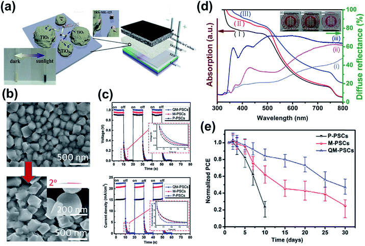 | ||
| Fig. 8 (a) Using TiO2-MIL-125 in a depleted heterojunction PVSC and its introduced photochromic effect (insert). Adapted from ref. 119. (b) The SEM images showed the improved crystallinity of perovskite film grown on the hier-TiO2 ETL. The shape and contact angle of hier-TiO2 are presented in the inserted figure. Adapted from ref. 134. (c) The time profiles of Voc and Jsc of the hier-TiO2-derived PVSCs during on–off cycles of illumination. Adopted from ref. 134. (d) Comparison of UV-vis and diffuse reflectivity spectra of (i) MAPbI3/c-TiO2, (ii) MAPbI3/npt-TiO2, and (iii) MAPbI3/hier-TiO2, and the photographs of (i) c-TiO2, (ii) npt-TiO2, and (iii) hier-TiO2. (e) Normalized PCEs of PVSCs using different TiO2 ETLs with aging time. Adapted from ref. 134. | ||
As inspired by this achievement based on TiO2 NPs (referred to as npt-TiO2), Hou et al. further prepared a porous hierarchical TiO2 nanostructure (hier-TiO2) by sintering MIL-125.134 hier-TiO2 partly inherits the ordered porosity of MIL-125 and forms a quasi-mesoscopic scaffold on the compact TiO2 layer with scattered distribution, which provides relatively larger space for the perovskite materials to grow on as compared to the reference TiO2. Benefitting from its rougher surface and the capillary effect, the interfacial contact with the perovskite was improved to reduce the associated nucleation barrier and thus to enable better crystallinity (Fig. 8b). Owing to the formation of large-size circular plates, the hier-TiO2 scaffold could enhance the light-scattering effect (haze effect) at wavelengths from 350–700 nm, as shown in the diffusion reflectance comparison in Fig. 8d. Moreover, such a hier-TiO2 ETL enabled a better charge-extraction efficiency in the device, as evidenced from the response of Voc and Jsc to illumination (Fig. 8c). Consequently, its derived n–i–p PVSC not only showed an enhancement in the PCE from 6.40% to 16.56% (Table 3) but also exhibited an improved moisture stability under 30% relative humidity (RH) at room temperature (Fig. 8e) due to the better anchoring of perovskite grains on the hier-TiO2 ETL.134
| Situation | MOFs | Configuration | V oc | J sc | FF | PCE | Ref. |
|---|---|---|---|---|---|---|---|
| Interface modifier | TiO2-MIL-125 | n–i–p | 0.85 | 10.90 | 0.69 | 6.4 | 119 |
| Hier-TiO2 | n–i–p | 1.01 | 22.81 | 0.72 | 16.6 | 134 | |
| ZIF-8 | n–i–p | 1.02 | 22.82 | 0.73 | 17.0 | 135 | |
| MOF-808 | p–i–n | 1.07 | 19.64 | 0.79 | 16.6 | 136 | |
| UiO-66 | p–i–n | 1.07 | 20.25 | 0.80 | 17.0 | 136 | |
| HTL | In2 | n–i–p | 1.01 | 21.03 | 0.74 | 15.8 | 138 |
| ETL | nTi-MOF | n–i–p (rigid) | 1.08 | 23.18 | 0.76 | 18.9 | 137 |
| n–i–p (flexible) | 1.05 | 22.61 | 0.73 | 17.4 | 137 | ||
| In the perovskite layer | MOF-525 | n–i–p | 0.93 | 23.04 | 0.60 | 12.0 | 139 |
| MOF-808 | p–i–n | 1.06 | 21.01 | 0.80 | 17.8 | 136 | |
| UiO-66 | p–i–n | 1.07 | 21.85 | 0.77 | 18.0 | 136 |
After these pioneering studies, versatile MOFs have been explored through the interface engineering of PVSCs. For example, Shen et al. introduced a type of insulating ZIF-8 upon the mesoporous TiO2 (mp-TiO2) layer, instead of making adjustment in the mesoporous TiO2 scaffold.135 Similar to the effects disclosed in the previous reports, the addition of ZIF-8 roughened the surface of the mp-TiO2 layer to promote the crystallinity of the perovskite layer grown on top as shown in Fig. 9a. Notably, they found that the formation of perovskite crystals is controlled by the competition between the primary nucleation and the following growth. If the surface of the ZIF-8/mp-TiO2 hybrid scaffold became too rough, it would hamper the growth of the perovskite. Hence, there is an optimum value of ZIF-8 coated on mp-TiO2. Besides the scaffold's ordered porosity, they also claimed that hydrogen bonding existed between ZIF-8 and the perovskite material, which partly contributes to the promoted crystallinity and quality of the perovskite film grown on top. Consequently, the hybrid ZIF-8/mp-TiO2 scaffold could possess an enhanced charge-extraction capability, as evidenced by the photoluminescence (PL) quenching (Fig. 9b).135
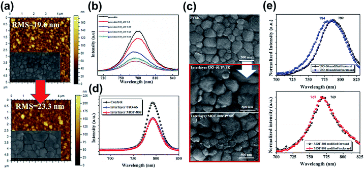 | ||
| Fig. 9 (a) The AFM images showed that ZIF-8 roughens the surface of the mp-TiO2 layer. The inserted SEM images are the corresponding morphology of the perovskite film grown on top of it. Adapted from ref. 135. (b) The PL spectra of the perovskite film grown on ZIF-8 with different coating times. Adapted from ref. 135. (c) The SEM images of the pristine MAPbI3, MAPbI3/UiO-66, and MAPbI3/MOF-808 films. Adapted from ref. 136. (d) The PL spectra for the perovskite film grown on UiO-66 and MOF-808. Adapted from ref. 136. (e) The PL spectra for the perovskite/UiO-66 and perovskite/MOF-808 samples illuminated from the perovskite side (forward) and the MOF side (backward). Adapted from ref. 136. | ||
Very recently, applying MOFs in inverted p–i–n PVSCs has also been reported. Different to the conventional n–i–p configuration, the inverted PVSCs were usually fabricated with a planar structure using PEDOT![[thin space (1/6-em)]](https://www.rsc.org/images/entities/char_2009.gif) :
:![[thin space (1/6-em)]](https://www.rsc.org/images/entities/char_2009.gif) PSS or inorganic NiOx as the hole-transporting layers (HTLs) that possess facile solution processability. Therefore, it can avoid the cumbersome fabrication techniques involved in conventional PVSC, possessing better potential for massive production.140 Given the planar architecture of the p–i–n device, Lee et al. inserted insulating porous Zr-MOFs, UiO-66 and MOF-808, at the NiOx/perovskite interface to provide an additional scaffold for the perovskite materials to grow on.136 Similar to the abovementioned benefits of the microporous scaffold, these inserted MOFs promote the crystallinity of the perovskite film grown on top (Fig. 9c). It is because they could allow the filling of the perovskite precursor at the NiOx/perovskite interface to enable better compatibility for crystal nucleation and crystallization. Besides, they also unveiled that the lone pair of the oxygen in the MOFs could coordinate with Pb2+ to modulate the crystallization rate of the perovskite. As a result, the charge-extraction efficiency at the NiOx/perovskite interface was enhanced as inferred from the PL quenching (Fig. 9d) and an improvement in PCE to 17.01% was realized (Table 3).136 Interestingly, the authors found a slight blue-shifted PL of the MOF/perovskite samples while illuminated at the MOF side (Fig. 9e). This result indicated that the perovskite materials close to the inserted MOFs possess a reduced defective state, revealing its functionality of defect passivation as a result of the improved crystallinity or the interaction between them.136
PSS or inorganic NiOx as the hole-transporting layers (HTLs) that possess facile solution processability. Therefore, it can avoid the cumbersome fabrication techniques involved in conventional PVSC, possessing better potential for massive production.140 Given the planar architecture of the p–i–n device, Lee et al. inserted insulating porous Zr-MOFs, UiO-66 and MOF-808, at the NiOx/perovskite interface to provide an additional scaffold for the perovskite materials to grow on.136 Similar to the abovementioned benefits of the microporous scaffold, these inserted MOFs promote the crystallinity of the perovskite film grown on top (Fig. 9c). It is because they could allow the filling of the perovskite precursor at the NiOx/perovskite interface to enable better compatibility for crystal nucleation and crystallization. Besides, they also unveiled that the lone pair of the oxygen in the MOFs could coordinate with Pb2+ to modulate the crystallization rate of the perovskite. As a result, the charge-extraction efficiency at the NiOx/perovskite interface was enhanced as inferred from the PL quenching (Fig. 9d) and an improvement in PCE to 17.01% was realized (Table 3).136 Interestingly, the authors found a slight blue-shifted PL of the MOF/perovskite samples while illuminated at the MOF side (Fig. 9e). This result indicated that the perovskite materials close to the inserted MOFs possess a reduced defective state, revealing its functionality of defect passivation as a result of the improved crystallinity or the interaction between them.136
4.2 MOFs as the charge-transporting layers
Besides being employed as the interface modifiers, MOFs have also been explored as the CTLs for PVSCs. It should be noted that the roles that MOFs play in the CTLs are very different from the previous case. Up to now, there have only been a few studies investigating the function of MOFs in CTLs,137,138 and the studied MOFs were all conductive and exploited in the conventional n–i–p PVSCs. Their influence on the device's charge-extraction efficiency, suppression of charge recombination, quality of the perovskite film, UV-region absorption, and the device's stability are discussed in common and more details are provided below.Very recently, Ryu et al. fabricated nanocrystalline Ti-based MOF (nTi-MOF) NPs on ITO glass via a solvothermal synthesis.137 With the assistance of high rates of heat transfer, nTi-MOF rather than Ti-MOF (MIL-125) was successfully obtained. Although the chemical state of Ti in nTi-MOF is similar to that of Ti in TiO2, their overall electronic structures were slightly different. As depicted in Fig. 10a, nTi-MOF possessed a higher transmittance than TiO2 owing to its wider Eg. Fig. 10b presents the energy level of nTi-MOF. As seen, its energy level matches well with those of the perovskite and ITO, indicating its potential to serve as an ETL in a device. However, owing to the existence of microcracks, the nTi-MOF film possessed a slightly lower conductivity (4.46 × 10⁻⁵ S cm−1) than the regular TiO2 (6.38 × 10⁻⁵ S cm−1). Consequently, its derived n–i–p device showed an unsatisfactory PCE of 16.41% after optimization. To further improve the device performance, the authors introduced an additional PCBM layer on top of nTi-MOF. It not only avoids the direct contact of ITO with the perovskite layer but also enhances the conductivity to 1.09 × 10⁻⁴ S cm−1. As shown in Fig. 10b, such a PCBM layer could also ensure a better band alignment at the perovskite/nTi-MOF interface, providing a synergetic effect with nTi-MOF in the ETL. As a result, the PCE of the derived device can be boosted to 18.94% (Table 3), which is the highest value reported for MOF-derived PVSCs to date.137
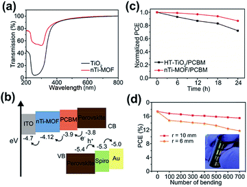 | ||
| Fig. 10 (a) The transmission of TiO2 and nTi-MOF. (b) The energy-level diagram and (c) photostability profile of the nTi-MOF derived PVSC. (d) Durability test of the nTi-MOF derived flexible PVSC. Adapted from ref. 137. | ||
Because the nTi-MOF/PCBM ETL can suppress the photocatalytic effect and nTi-MOF can effectively absorb UV radiation owing to its large Eg, the derived PVCS was demonstrated to possess a better photostability compared to the device using a regular TiO2 ETL, as portrayed in Fig. 10c. Moreover, because the nanostructured nTi-MOF was composed of titanium oxide units spatially linked, it is feasible to use it for fabricating the flexible device. Finally, a flexible PVSC using the nTi-MOF/PCBM ETL is demonstrated to show a promising PCE of 17.43% and could endure up to 700 cycles of bending at different radii, as presented in Fig. 10d. This work represents the first example of MOF-base flexible PVSCs.137
Besides using MOF in the ETL, Li et al. recently have doped a indium-based MOF, [In2(phen)3Cl6]·CH3CN·2H2O (In2), into the Spiro-OMeTAD HTL.138 Different from the previous case reported by Ryu et al.,137 In2 was directly blended into the Spiro-OMeTAD precursor and fabricated on top of the perovskite layer. The authors first manifested that the addition of In2 into the HTL can provide additional photo-response for a device. On one hand, owing to the large Eg, In2 possesses an intense UV absorption while its emission was located in the visible-light region (Fig. 11a). This contributes to the absorption enhancement in the region across 320 nm to 540 nm as shown in Fig. 11b. On the other hand, the cube-like crystals of In2 in the HTL could act as the light-scattering center, which causes multiple reflections in the device to extend the light path length. This contributes to the absorption enhancement in the region from 500 nm to 700 nm (Fig. 11b).
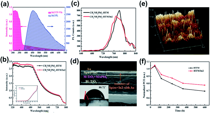 | ||
| Fig. 11 (a) The UV-vis and PL spectra of In2. (b) The UV-vis and (c) PL spectra of the perovskite-HTM and perovskite-HTM/In2 films. (d) The cross-section SEM image of the device using HTM/In2 as the HTL and the inset is the contact angle of the HTM/In2 HTL. (e) 3D analysis AFM image of the HTM/In2 HTL. (f) The stability profile for the control device and the device using the HTM/In2 HTL. Adapted from ref. 138. | ||
Meanwhile, the molecular structure of In2 possesses π–π stacking interactions, in which van der Waals forces were formed between chlorine and hydrogen. Such a strengthened conjugated system is beneficial for charge transport, as evidenced by the PL quenching (Fig. 11c). Note that the little blue-shifted PL shown in Fig. 11c indicated the passivation of the perovskite layer, which was attributed to the better film quality of the In2-doped HTL. The authors claimed that the blended In2 plugs the gaps inside the hole-transporting material (HTM; it is Spiro-OMeTAD herein) to enable a denser and less pin-hole morphology, as confirmed by the clear boundary at the interface shown in Fig. 11d. Thus, it can effectively prevent Au diffusion and oxygen penetration since In2 stands up like a shelter forest on Spiro-OMeTAD (Fig. 11e). Besides, the coverage of In2 on Spiro-OMeTAD resulted in a more hydrophobic surface (insert in Fig. 11d) to simultaneously prevent moisture penetration. Combing these advantages, the derived PVSC not only possessed a decent PCE of 15.80% (Table 3) with an obviously increased photocurrent but also showed an improved ambient stability under 40–45% RH at room temperature as exhibited in Fig. 11f.138
4.3 Perovskite/MOF heterojunction
Provided the regular microporous nature, Chang et al. blended Zr-based MOF-525 nanocrystals into the perovskite precursor at various ratios with the expectation to derive a uniform grain size and ordered arrangement.139 The hybrid perovskite/MOF-525 layer was fabricated on a compact TiO2 layer, and XPS depth profiling revealed that MOF-525 nanocrystals tend to be incorporated near the bottom side of the hybrid film (Fig. 12a). This result thus suggests that the hybrid film behaved more like the “meso-scaffold”, which allowed the perovskite precursor to diffuse into the pores at the interface with TiO2 to enable better crystallization of the perovskite film, as evidenced by the blue-shifted PL emission observed in Fig. 12b. The authors thus proposed the advantage of MOF scaffolds in the initial stage of crystallization of the perovskite films.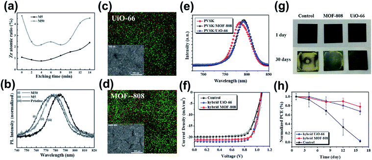 | ||
| Fig. 12 (a). Atomic ratio of Zr measured by XPS by Ar etching. Adapted from ref. 139. (b) Normalized PL spectra of the pristine perovskite and MOF-525/perovskite hybrid films. Adapted from ref. 139. (c and d) The SEM and SEM-EDS images (red is I and green is Zr) and (e) the PL spectra of the perovskite/MOF hybrid films. Adapted from ref. 136. (f) The J–V curves of the MOF-hybrid PVSCs. Adapted from ref. 136. (g) The real images of the aged films under ambient conditions. Adapted from ref. 136. (h) The stability test of the MOF-hybrid devices and the control device. Adapted from ref. 136. | ||
Furthermore, they demonstrated that the hybrid MOF-525 mainly played the role of a morphology modifier and crystallization enhancer, which does not change the semiconducting properties of the perovskite materials owing to its insulating property. Finally, the PVSC derived from such a hybrid film can deliver a PCE of 12.0% (Table 3), reflecting the potential of the perovskite/MOFs heterojunction in photovoltaic applications. However, the authors noted that the moisture instability of the device was unsolved because of the Spiro-OMeTAD HTL. Besides MOF-525, the authors have tried to fabricate the perovskite/MOF heterojunction using other Zr-based MOFs, like UiO-66 and UiO-67. It was shown that the UiO-66 hybrid yields a poor performance while the UiO-67 hybrid resulted in comparable performance to MOF-525. They attributed this discrepancy in the PCE to the different pore sizes of the employed MOFs, for which the larger pore sizes of UiO-67 relative to UiO-66 are favorable for the diffusion of the perovskite precursor to enable better performance.
Interestingly, very recently, Lee et al. partially addressed this problem and reported high-performance PVSCs based on the perovskite/UiO-66 and perovskite/MOF-808 hybrids.136 It should be noted that the perovskite processing technique and the device configuration used in these two studies are different, which might be the main reason causing the huge difference in the reported results. This is not surprising since the solution chemistry of perovskite precursors and the ensuing processing of perovskite films have been proven as a complicated procedure.141
Different from the previous study, Lee et al. blended UiO-66 and MOF-808 into the perovskite precursor at a very dilute concentration, and the hybrid films were deposited directly on the NiOx HTL to fabricate inverted p–i–n PVSCs. The full penetration of the perovskite into the MOF pores without separation could be confirmed by the obvious shrink in the grain size (Fig. 12c and d); meanwhile, the Zr atoms belonging to the hybrid MOFs seem to distribute around the perovskite grain boundaries as seen in the corresponding SEM-EDS image, limiting the growth of perovskite crystals. Since the lone pairs on the oxygen of UiO-66 and MOF-808 could coordinate with the Pb2+ atoms of perovskite, the function of defect passivation was also suggested, as inferred from the increased PL intensity (Fig. 12e). On the other hand, because the porous architecture of MOFs can accommodate the filling of the perovskite, the charge-transport pathways might be across the hybrid MOFs' scaffold. Benefitting from these advantages, the perovskite/UiO-66 hybrid device delivered a high PCE of 18.01% (Table 3) without severe hysteresis (Fig. 12f). Note that the resulting performance of the MOF-hybrid device surpasses the value of the device using the MOF at the perovskite/HTL interface, showing the potential of the perovskite/MOF heterojunction in photovoltaic applications. The authors have further investigated the stability of these MOF-hybrid devices. It was revealed that the hybrid MOFs seem to offer the grain-locking effect to prohibit moisture invasion, which reinforces the film's ambient stability (60 ± 5% RH at room temperature) as shown in Fig. 12g. As a result, the unencapsulated MOF-hybrid devices showed a much improved ambient stability compared to the pristine device, as illustrated in Fig. 12h.
In summary, due to the solution-processability and microporous structure, MOFs have attracted increasing research attention for applications in PVSCs. Besides, given their good chemical and thermal stability, MOFs have also been proven to improve the long-term stability of the derived devices. Based on the abovementioned research studies, three main points can be concluded: (i) the MOFs can improve the quality and crystallinity of the perovskite film regardless of being used as the interface modifier or being blended in the perovskite layer, (ii) the MOFs can enhance the charge transfer across associated interfaces and prohibit charge recombination to a certain degree regardless of being used as the interface modifier or being blended in the perovskite layer, and (iii) the perovskite/MOFs heterojunction possesses improved ambient stability. These characteristics illuminate the roles that MOFs can play in the future development of PVSCs. Meanwhile, it is worth noting that most of the MOFs possess a wide Eg that can absorb UV radiation. That said, while using MOFs in the photovoltaic device, they might provide additional photo-response or functions, such as UV-filtering, light scattering, photochromic effects, and down-conversion of high-energy photons through energy transfer that definitely warrant more detailed investigation in the future.
5. MOFs in organic solar cells (OSCs)
In contrast to the growing applications in DSSCs and PVSCs, MOFs have not been widely explored in OSCs yet and relevant studies are quite rare thus far. As mentioned earlier, the direct use of MOFs as the photoactive materials is quite challenging. Besides, owing to the inferior semiconducting properties of organic materials than the inorganic counterpart, the applications of MOFs in OSCs are restricted to interlayer engineering. Very recently, Huang et al. fabricated novel 2D tellurophene-based MOFs, which were exfoliated by branched poly(ethylenimine) ethoxylate (PEIE) to form single- or few-layer MOF nanosheets, and employed them as an electron-extraction layer (EEL) in OSCs.142 It was revealed that such a hybrid EEL could possess improved conductivity than pristine PEIE and tune the work function of the ETL to suppress the charge recombination in the derived device, enabling a 15% enhancement in the PCE in comparison to the control device as shown in Fig. 13.142 This result signifies the possible advantages of MOFs in interlayer modification, which might promote the future development of MOFs in OSCs.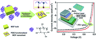 | ||
| Fig. 13 Schematic illustration of the preparation of 2D MOF nanosheets and their modified electron-extraction layer for photovoltaic devices. Adapted from ref. 142. | ||
6. Conclusion
In summary, utilizing MOFs and MOF-derived materials in photovoltaic applications has become an emerging subfield in recent years. Engineering the structures of MOFs to afford suitable Egs and satisfactory semiconducting properties has been continuously explored at both simulation and experimental levels to improve the photovoltaic properties of MOFs themselves. Meanwhile, several research efforts have focused on the use of MOF materials in DSSCs, PVSCs, and OSCs to enhance their performance and stability.Many efforts have been made to utilize MOFs in DSSCs. For the photoanodes in DSSCs, using MOFs or MOF-derived materials as the light scattering layers of photoanodes has shown promising enhancement in the power conversion efficiency. However, the direct use of MOFs constructed from photosensitizing units as the materials for photoanodes usually results in a poor cell efficiency, presumably due to the sluggish charge transport present in these electrically insulating frameworks. Utilizing MOF-derived materials as the electrocatalysts in the CEs of DSSCs is another choice to enhance the cell performance. Numerous studies have shown that porous carbons, metal sulphides, metal selenides, and metal carbides derived from MOFs can be used as materials for CEs and achieve promising cell performance, which indicates that these MOF-derived materials should be considered as the next-generation CE materials to replace conventional Pt.
For the application in PVSVs, the benefits of using MOFs as the interface modifier or additive in the device have been proved, including improved perovskite film quality/crystallinity, enhanced long-term stability, and promoted charge transfer and special photo-response. However, the precise interaction between MOFs and perovskites or employed CTLs and its actual mechanism remain unsolved and more insightful investigations are required to further expand the widespread applications of MOFs in PVSCs. Since the Egs and semiconducting properties of MOFs and their derivatives could be tuned by selecting electron-rich metal nodes/conjugation-based organic molecules, functionalizing the organic linker with electron-donating groups, and increasing the conjugation of the organic linker. Diverse functional MOFs are expected to be widely exploited for PVSCs in the near future. Meanwhile, although few studies have been reported so far, functional MOFs and their derivatives are also expected to be employed in OSCs to improve device performance and stability, provided their good physical/chemical stability and the success are demonstrated in the PVSCs.
7. Outlooks
7.1 Long-range charge transportation in MOFs
For pristine MOFs, although their bandgap (Eg) can be designed and reduced, it is still very difficult to realize long-range charge transport within most MOFs due to the high degree of charge localization in the three-dimensional rigid framework. Thus, it is quite challenging to directly utilize MOFs as the photoactive materials in practical photovoltaic devices. As mentioned previously, the direct use of MOFs consisting of photoactive units for the photoanodes in DSSCs generally resulted in a limited power conversion efficiency. Designing electrically conducting MOFs with proper photoactive units is one of the solutions for photovoltaic applications, but the examples of electrically conducting MOFs are still very limited to date; research efforts on developing more functional conducting MOFs are still required.7.2 Fine tuning MOFs with desired functionality
MOF crystals can serve as interface modifiers or additives in photovoltaic devices to enhance the performance and stability. The highly ordered and interconnected porosity of MOFs can alter the adsorption/desorption behavior of ionic species, adjust the light-harvesting properties, or improve the crystallization of the photoactive materials (e.g., perovskite in PVSCs) to enable better charge transfer in the device. Conceptually, it is more similar to the design of nanocomposites to integrate the functions of photoactive materials and the advantages of the porous MOFs. Consequently, the control of the functionality in the synthesized MOFs is both scientifically important and technologically useful for applying MOFs in photovoltaic cells.7.3 Development of MOF-derived materials
To design and synthesize MOF-derived materials would create another possibility to increase the performance of practical photovoltaic devices. Although MOF-derived materials are less structurally characterizable due to the loss of long-range order and regular porosity, they can resolve the issue of sluggish charge transport presented in most pristine MOFs while retaining suitable porosity. This fact makes MOF-derived materials remarkable electrode materials in photovoltaic devices like DSSCs. Several recent findings have indicated that DSSCs fabricated with MOF-derived CEs achieved significantly higher power conversion efficiencies compared to those fabricated with Pt-CEs, which suggests that MOFs are promising precursor materials to prepare MOF-derived CEs for practical high-performance DSSCs.Conflicts of interest
There are no conflicts to declare.Acknowledgements
This work was supported by the Ministry of Science and Technology (MOST) of Taiwan, under projects 108-3017-F-002-002, 106-2218-E-002-021-MY2, 105-2221-E-002-003-MY3, and 107-2218-E-006-054-MY3. We also thank the support from Ministry of Education (MOE) in Taiwan (grant number: 108L9006) and National Taiwan University (grant numbers: 107L7846 and 107L104312). C.-W. K. thank the support from the Yushan Young Scholar Program under MOE, Taiwan.Notes and references
- G. Ferey, Chem. Soc. Rev., 2008, 37, 191–214 RSC.
- H. Furukawa, K. E. Cordova, M. O'Keeffe and O. M. Yaghi, Science, 2013, 341, 1230444 CrossRef PubMed.
- S. Kitagawa, R. Kitaura and S.-i. Noro, Angew. Chem., Int. Ed., 2004, 43, 2334–2375 CrossRef CAS PubMed.
- O. K. Farha, I. Eryazici, N. C. Jeong, B. G. Hauser, C. E. Wilmer, A. A. Sarjeant, R. Q. Snurr, S. T. Nguyen, A. O. Yazaydin and J. T. Hupp, J. Am. Chem. Soc., 2012, 134, 15016–15021 CrossRef CAS PubMed.
- I. M. Hönicke, I. Senkovska, V. Bon, I. A. Baburin, N. Bönisch, S. Raschke, J. D. Evans and S. Kaskel, Angew. Chem., Int. Ed., 2018, 57, 13780–13783 CrossRef PubMed.
- B. F. Hoskins and R. Robson, J. Am. Chem. Soc., 1989, 111, 5962–5964 CrossRef CAS.
- B. F. Hoskins and R. Robson, J. Am. Chem. Soc., 1990, 112, 1546–1554 CrossRef CAS.
- O. M. Yaghi, G. M. Li and H. L. Li, Nature, 1995, 378, 703–706 CrossRef CAS.
- M. Kondo, T. Yoshitomi, K. Seki, H. Matsuzaka and S. Kitagawa, Angew. Chem., Int. Ed., 1997, 36, 1725–1727 CrossRef CAS.
- C. Livage, C. Egger and G. Ferey, Chem. Mater., 1999, 11, 1546–1550 CrossRef CAS.
- H. Li, M. Eddaoudi, T. L. Groy and O. M. Yaghi, J. Am. Chem. Soc., 1998, 120, 8571–8572 CrossRef CAS.
- M. J. Kalmutzki, N. Hanikel and O. M. Yaghi, Sci. Adv., 2018, 4, eaat9180 CrossRef PubMed.
- N. Stock and S. Biswas, Chem. Rev., 2012, 112, 933–969 CrossRef CAS PubMed.
- A. J. Howarth, Y. Liu, P. Li, Z. Li, T. C. Wang, J. T. Hupp and O. K. Farha, Nat. Rev. Mater., 2016, 1, 15018 CrossRef CAS.
- N. C. Burtch, H. Jasuja and K. S. Walton, Chem. Rev., 2014, 114, 10575–10612 CrossRef CAS PubMed.
- Z. Liang, C. Qu, W. Guo, R. Zou and Q. Xu, Adv. Mater., 2018, 30, 1702891 CrossRef PubMed.
- M. B. Majewski, A. W. Peters, M. R. Wasielewski, J. T. Hupp and O. K. Farha, ACS Energy Lett., 2018, 3, 598–611 CrossRef CAS.
- Y. Z. Chen, R. Zhang, L. Jiao and H. L. Jiang, Coord. Chem. Rev., 2018, 362, 1–23 CrossRef CAS.
- B. You, N. Jiang, M. Sheng, W. S. Drisdell, J. Yano and Y. Sun, ACS Catal., 2015, 5, 7068–7076 CrossRef CAS.
- P. Yin, T. Yao, Y. Wu, L. Zheng, Y. Lin, W. Liu, H. Ju, J. Zhu, X. Hong, Z. Deng, G. Zhou, S. Wei and Y. Li, Angew. Chem., Int. Ed., 2016, 55, 10800–10805 CrossRef CAS PubMed.
- L. J. Murray, M. Dinca and J. R. Long, Chem. Soc. Rev., 2009, 38, 1294–1314 RSC.
- D. Alezi, Y. Belmabkhout, M. Suyetin, P. M. Bhatt, Ł. J. Weseliński, V. Solovyeva, K. Adil, I. Spanopoulos, P. N. Trikalitis, A.-H. Emwas and M. Eddaoudi, J. Am. Chem. Soc., 2015, 137, 13308–13318 CrossRef CAS PubMed.
- Y. He, W. Zhou, G. Qian and B. Chen, Chem. Soc. Rev., 2014, 43, 5657–5678 RSC.
- M. G. Campbell and M. Dincă, Sensors, 2017, 17, 1108 CrossRef PubMed.
- L. E. Kreno, K. Leong, O. K. Farha, M. Allendorf, R. P. Van Duyne and J. T. Hupp, Chem. Rev., 2012, 112, 1105–1125 CrossRef CAS PubMed.
- J.-R. Li, J. Sculley and H.-C. Zhou, Chem. Rev., 2012, 112, 869–932 CrossRef CAS PubMed.
- S. Qiu, M. Xue and G. Zhu, Chem. Soc. Rev., 2014, 43, 6116–6140 RSC.
- J. Lee, O. K. Farha, J. Roberts, K. A. Scheidt, S. T. Nguyen and J. T. Hupp, Chem. Soc. Rev., 2009, 38, 1450–1459 RSC.
- L. Ma, C. Abney and W. Lin, Chem. Soc. Rev., 2009, 38, 1248–1256 RSC.
- S. M. Cohen, Chem. Rev., 2012, 112, 970–1000 CrossRef CAS PubMed.
- T. Islamoglu, S. Goswami, Z. Li, A. J. Howarth, O. K. Farha and J. T. Hupp, Acc. Chem. Res., 2017, 50, 805–813 CrossRef CAS PubMed.
- C.-W. Kung, K. Otake, C. T. Buru, S. Goswami, Y. Cui, J. T. Hupp, A. M. Spokoyny and O. K. Farha, J. Am. Chem. Soc., 2018, 140, 3871–3875 CrossRef CAS PubMed.
- A. A. Talin, A. Centrone, A. C. Ford, M. E. Foster, V. Stavila, P. Haney, R. A. Kinney, V. Szalai, F. El Gabaly, H. P. Yoon, F. Léonard and M. D. Allendorf, Science, 2014, 343, 66–69 CrossRef CAS PubMed.
- G. Lu, S. Li, Z. Guo, O. K. Farha, B. G. Hauser, X. Qi, Y. Wang, X. Wang, S. Han, X. Liu, J. S. DuChene, H. Zhang, Q. Zhang, X. Chen, J. Ma, S. C. J. Loo, W. D. Wei, Y. Yang, J. T. Hupp and F. Huo, Nat. Chem., 2012, 4, 310–316 CrossRef CAS PubMed.
- C.-H. Kuo, Y. Tang, L.-Y. Chou, B. T. Sneed, C. N. Brodsky, Z. Zhao and C.-K. Tsung, J. Am. Chem. Soc., 2012, 134, 14345–14348 CrossRef CAS PubMed.
- F.-K. Shieh, S.-C. Wang, C.-I. Yen, C.-C. Wu, S. Dutta, L.-Y. Chou, J. V. Morabito, P. Hu, M.-H. Hsu, K. C. W. Wu and C.-K. Tsung, J. Am. Chem. Soc., 2015, 137, 4276–4279 CrossRef CAS PubMed.
- X. Lian, Y. Fang, E. Joseph, Q. Wang, J. Li, S. Banerjee, C. Lollar, X. Wang and H.-C. Zhou, Chem. Soc. Rev., 2017, 46, 3386–3401 RSC.
- L. Jiao, Y. Wang, H. L. Jiang and Q. Xu, Adv. Mater., 2018, 30, 1703663 CrossRef PubMed.
- Y. T. Liao, B. M. Matsagar and K. C. W. Wu, ACS Sustainable Chem. Eng., 2018, 6, 13628–13643 CrossRef CAS.
- Y. V. Kaneti, S. Dutta, M. S. A. Hossain, M. J. A. Shiddiky, K. L. Tung, F. K. Shieh, C. K. Tsung, K. C. W. Wu and Y. Yamauchi, Adv. Mater., 2017, 29, 1700213 CrossRef PubMed.
- J. D. Sosa, T. F. Bennett, K. J. Nelms, B. M. Liu, R. C. Tovar and Y. Y. Liu, Crystals, 2018, 8, 325 CrossRef.
- Z. Zhang, H. T. H. Nguyen, S. A. Miller and S. M. Cohen, Angew. Chem., Int. Ed., 2015, 54, 6152–6157 CrossRef CAS PubMed.
- E. R. Parnham and R. E. Morris, Acc. Chem. Res., 2007, 40, 1005–1013 CrossRef CAS PubMed.
- B. You, N. Jiang, M. Sheng, S. Gul, J. Yano and Y. Sun, Chem. Mater., 2015, 27, 7636–7642 CrossRef CAS.
- X. Liu, J. Dong, B. You and Y. Sun, RSC Adv., 2016, 6, 73336–73342 RSC.
- K. Shen, X. Chen, J. Chen and Y. Li, ACS Catal., 2016, 6, 5887–5903 CrossRef CAS.
- M. H. Yap, K. L. Fow and G. Z. Chen, Green Energy & Environment, 2017, 2, 218–245 Search PubMed.
- M. Hu, J. Reboul, S. Furukawa, N. L. Torad, Q. M. Ji, P. Srinivasu, K. Ariga, S. Kitagawa and Y. Yamauchi, J. Am. Chem. Soc., 2012, 134, 2864–2867 CrossRef CAS PubMed.
- L.-M. Yang, P. Vajeeston, P. Ravindran, H. Fjellvåg and M. Tilset, Inorg. Chem., 2010, 49, 10283–10290 CrossRef CAS PubMed.
- B. Civalleri, F. Napoli, Y. Noël, C. Roetti and R. Dovesi, CrystEngComm, 2006, 8, 364–371 RSC.
- J. J. Perry IV, P. L. Feng, S. T. Meek, K. Leong, F. P. Doty and M. D. Allendorf, J. Mater. Chem., 2012, 22, 10235–10248 RSC.
- C. A. Bauer, T. V. Timofeeva, T. B. Settersten, B. D. Patterson, V. H. Liu, B. A. Simmons and M. D. Allendorf, J. Am. Chem. Soc., 2007, 129, 7136–7144 CrossRef CAS PubMed.
- N. L. Rosi, J. Kim, M. Eddaoudi, B. Chen, M. O'Keeffe and O. M. Yaghi, J. Am. Chem. Soc., 2005, 127, 1504–1518 CrossRef CAS PubMed.
- J. Yang, C. Zheng, P. Xiong, Y. Li and M. Wei, J. Mater. Chem. A, 2014, 2, 19005–19010 RSC.
- M. Tu and R. A. Fischer, J. Mater. Chem. A, 2014, 2, 2018–2022 RSC.
- M. Fuentes-Cabrera, D. M. Nicholson, B. G. Sumpter and M. Widom, J. Chem. Phys., 2005, 123, 124713 CrossRef PubMed.
- P. Sippel, D. Denysenko, A. Loidl, P. Lunkenheimer, G. Sastre and D. Volkmer, Adv. Funct. Mater., 2014, 24, 3885–3896 CrossRef CAS.
- C. H. Hendon, D. Tiana, M. Fontecave, C. m. Sanchez, L. D’arras, C. Sassoye, L. Rozes, C. Mellot-Draznieks and A. Walsh, J. Am. Chem. Soc., 2013, 135, 10942–10945 CrossRef CAS PubMed.
- T. Musho, J. Li and N. Wu, Phys. Chem. Chem. Phys., 2014, 16, 23646–23653 RSC.
- K. Leong, M. E. Foster, B. M. Wong, E. D. Spoerke, D. Van Gough, J. C. Deaton and M. D. Allendorf, J. Mater. Chem. A, 2014, 2, 3389–3398 RSC.
- S. Goswami, J. N. Nelson, T. Islamoglu, Y.-L. Wu, O. K. Farha and M. R. Wasielewski, Chem. Mater., 2018, 30, 2488–2492 CrossRef CAS.
- Z. Guo, D. K. Panda, M. A. Gordillo, A. Khatun, H. Wu, W. Zhou and S. Saha, ACS Appl. Mater. Interfaces, 2017, 9, 32413–32417 CrossRef CAS PubMed.
- M. Usman, S. Mendiratta, S. Batjargal, G. Haider, M. Hayashi, N. Rao Gade, J.-W. Chen, Y.-F. Chen and K.-L. Lu, ACS Appl. Mater. Interfaces, 2015, 7, 22767–22774 CrossRef CAS PubMed.
- M. Usman, S. Mendiratta and K. L. Lu, Adv. Mater., 2017, 29, 1605071 CrossRef PubMed.
- B. O'Regan and M. Grätzel, Nature, 1991, 353, 737–740 CrossRef.
- G. Hashmi, K. Miettunen, T. Peltola, J. Halme, I. Asghar, K. Aitola, M. Toivola and P. Lund, Renewable Sustainable Energy Rev., 2011, 15, 3717–3732 CrossRef CAS.
- A. Hagfeldt, G. Boschloo, L. Sun, L. Kloo and H. Pettersson, Chem. Rev., 2010, 110, 6595–6663 CrossRef CAS PubMed.
- A. Morozan and F. Jaouen, Energy Environ. Sci., 2012, 5, 9269–9290 RSC.
- C. H. Hendon, D. Tiana and A. Walsh, Phys. Chem. Chem. Phys., 2012, 14, 13120–13132 RSC.
- L. Sun, M. G. Campbell and M. Dincă, Angew. Chem., Int. Ed., 2016, 55, 3566–3579 CrossRef CAS PubMed.
- S. Lin, P. M. Usov and A. J. Morris, Chem. Commun., 2018, 54, 6965–6974 RSC.
- Y. Li, A. Pang, C. Wang and M. Wei, J. Mater. Chem., 2011, 21, 17259–17264 RSC.
- H. A. Lopez, A. Dhakshinamoorthy, B. Ferrer, P. Atienzar, M. Alvaro and H. Garcia, J. Phys. Chem. C, 2011, 115, 22200–22206 CrossRef CAS.
- R. Kaur, K.-H. Kim, A. K. Paul and A. Deep, J. Mater. Chem. A, 2016, 4, 3991–4002 RSC.
- Y. Li, C. Chen, X. Sun, J. Dou and M. Wei, ChemSusChem, 2014, 7, 2469–2472 CrossRef CAS PubMed.
- A. Gu, W. Xiang, T. Wang, S. Gu and X. Zhao, Sol. Energy, 2017, 147, 126–132 CrossRef CAS.
- D. Y. Lee, D. V. Shinde, S. J. Yoon, K. N. Cho, W. Lee, N. K. Shrestha and S.-H. Han, J. Phys. Chem. C, 2014, 118, 16328–16334 CrossRef CAS.
- D. Y. Lee, E.-K. Kim, C. Y. Shin, D. V. Shinde, W. Lee, N. K. Shrestha, J. K. Lee and S.-H. Han, RSC Adv., 2014, 4, 12037–12042 RSC.
- J. Liu, W. Zhou, J. Liu, I. Howard, G. Kilibarda, S. Schlabach, D. Coupry, M. Addicoat, S. Yoneda, Y. Tsutsui, T. Sakurai, S. Seki, Z. Wang, P. Lindemann, E. Redel, T. Heine and C. Wöll, Angew. Chem., Int. Ed., 2015, 54, 7441–7445 CrossRef CAS PubMed.
- W. A. Maza, A. J. Haring, S. R. Ahrenholtz, C. C. Epley, S. Y. Lin and A. J. Morris, Chem. Sci., 2016, 7, 719–727 RSC.
- E. D. Spoerke, L. J. Small, M. E. Foster, J. Wheeler, A. M. Ullman, V. Stavila, M. Rodriguez and M. D. Allendorf, J. Phys. Chem. C, 2017, 121, 4816–4824 CrossRef CAS.
- R. Kaur, K.-H. Kim and A. Deep, Appl. Surf. Sci., 2017, 396, 1303–1309 CrossRef CAS.
- S. Ahmad, J. Liu, W. Ji and L. Sun, Materials, 2018, 11, 1868 CrossRef PubMed.
- X. Du, R. Fan, X. Wang, G. Yu, L. Qiang, P. Wang, S. Gao and Y. Yang, Cryst. Growth Des., 2016, 16, 1737–1745 CrossRef CAS.
- J. Zhu, W. A. Maza and A. J. Morris, J. Photochem. Photobiol., A, 2017, 344, 64–77 CrossRef CAS.
- M. Wu and T. Ma, ChemSusChem, 2012, 5, 1343–1357 CrossRef CAS PubMed.
- J. Wu, Z. Lan, J. Lin, M. Huang, Y. Huang, L. Fan, G. Luo, Y. Lin, Y. Xie and Y. Wei, Chem. Soc. Rev., 2017, 46, 5975–6023 RSC.
- S. Thomas, T. G. Deepak, G. S. Anjusree, T. A. Arun, S. V. Nair and A. S. Nair, J. Mater. Chem. A, 2014, 2, 4474–4490 RSC.
- T.-Y. Chen, Y.-J. Huang, C.-T. Li, C.-W. Kung, R. Vittal and K.-C. Ho, Nano Energy, 2017, 32, 19–27 CrossRef CAS.
- A. S. A. Ahmed, W. Xiang, I. Saana Amiinu and X. Zhao, New J. Chem., 2018, 42, 17303–17310 RSC.
- I. Concina and A. Vomiero, Small, 2015, 11, 1744–1774 CrossRef CAS PubMed.
- T. Kundu, S. C. Sahoo and R. Banerjee, Cryst. Growth Des., 2012, 12, 2572–2578 CrossRef CAS.
- T. Enomoto, S. Ueno, E. Hosono, M. Hagiwara and S. Fujihara, CrystEngComm, 2017, 19, 2844–2851 RSC.
- Q. Liu, Z.-X. Low, Y. Feng, S. Leong, Z. Zhong, J. Yao, K. Hapgood and H. Wang, Microporous Mesoporous Mater., 2014, 194, 1–7 CrossRef CAS.
- J. Dou, Y. Li, F. Xie, X. Ding and M. Wei, Cryst. Growth Des., 2016, 16, 121–125 CrossRef CAS.
- R. Tang, Z. Xie, S. Zhou, Y. Zhang, Z. Yuan, L. Zhang and L. Yin, ACS Appl. Mater. Interfaces, 2016, 8, 22201–22212 CrossRef CAS PubMed.
- R. Tang, R. Yin, S. Zhou, T. Ge, Z. Yuan, L. Zhang and L. Yin, J. Mater. Chem. A, 2017, 5, 4962–4971 RSC.
- S. Yuan, J.-S. Qin, C. T. Lollar and H.-C. Zhou, ACS Cent. Sci., 2018, 4, 440–450 CrossRef CAS PubMed.
- W. S. Chi, D. K. Roh, C. S. Lee and J. H. Kim, J. Mater. Chem. A, 2015, 3, 21599–21608 RSC.
- Y. Li, Z. Che, X. Sun, J. Dou and M. Wei, Chem. Commun., 2014, 50, 9769–9772 RSC.
- X. Zheng, W. Chen, L. Chen, Y. Wang, X. Guo, J. Wang and E. Wang, Chem.–Eur. J., 2017, 23, 8871–8878 CrossRef CAS PubMed.
- S.-H. Hsu, C.-T. Li, H.-T. Chien, R. R. Salunkhe, N. Suzuki, Y. Yamauchi, K.-C. Ho and K. C. W. Wu, Sci. Rep., 2014, 4, 6983 CrossRef CAS PubMed.
- X. Sun, Y. Li, J. Dou, D. Shen and M. Wei, J. Power Sources, 2016, 322, 93–98 CrossRef CAS.
- M.-S. Wu, C.-Y. Chen, Y.-R. Chen and H.-C. Shih, Electrochim. Acta, 2016, 215, 50–56 CrossRef CAS.
- H. Jing, X. Song, S. Ren, Y. Shi, Y. An, Y. Yang, M. Feng, S. Ma and C. Hao, Electrochim. Acta, 2016, 213, 252–259 CrossRef CAS.
- Z. Xie, X. Cui, W. Xu and Y. Wang, Electrochim. Acta, 2017, 229, 361–370 CrossRef CAS.
- S. H. Ahn, C. H. Lee, M. S. Kim, S. A. Kim, B. Kang, H.-e. Kim, S. U. Lee and J. H. Bang, J. Phys. Chem. C, 2017, 121, 27332–27343 CrossRef CAS.
- A. S. A. Ahmed, W. Xiang, Z. Li, I. S. Amiinu and X. Zhao, Electrochim. Acta, 2018, 292, 276–284 CrossRef CAS.
- J. S. Kang, J. Kang, D. Y. Chung, Y. J. Son, S. Kim, S. Kim, J. Kim, J. Jeong, M. J. Lee, H. Shin, S. Park, S. J. Yoo, M. J. Ko, J. Yoon and Y.-E. Sung, J. Mater. Chem. A, 2018, 6, 20170–20183 RSC.
- J. Ou, C. Gong, J. Xiang and J. Liu, Sol. Energy, 2018, 174, 225–230 CrossRef CAS.
- J. Ou, C. Gong, M. Wang, J. Xiang and J. Liu, Electrochim. Acta, 2018, 286, 212–218 CrossRef CAS.
- X. Jiang, H. Li, S. Li, S. Huang, C. Zhu and L. Hou, Chem. Eng. J., 2018, 334, 419–431 CrossRef CAS.
- X. Cui, Z. Xie and Y. Wang, Nanoscale, 2016, 8, 11984–11992 RSC.
- C. Xu, J. Zhang, X. Qian, W. Wu, J. Yang and L. Hou, Electrochim. Acta, 2018, 289, 448–458 CrossRef CAS.
- S.-L. Jian, Y.-J. Huang, M.-H. Yeh and K.-C. Ho, J. Mater. Chem. A, 2018, 6, 5107–5118 RSC.
- W. Lu, R. Jiang, X. Yin and L. Wang, Nano Res., 2019, 12, 159–163 CrossRef CAS.
- L. Chen, W. Chen and E. Wang, J. Power Sources, 2018, 380, 18–25 CrossRef CAS.
- F. Bella, R. Bongiovanni, R. S. Kumar, M. A. Kulandainathan and A. M. Stephan, J. Mater. Chem. A, 2013, 1, 9033–9036 RSC.
- A. V. Vinogradov, H. Zaake-Hertling, E. Hey-Hawkins, A. V. Agafonov, G. A. Seisenbaeva, V. G. Kessler and V. V. Vinogradov, Chem. Commun., 2014, 50, 10210–10213 RSC.
- N. J. Jeon, H. Na, E. H. Jung, T.-Y. Yang, Y. G. Lee, G. Kim, H.-W. Shin, S. I. Seok, J. Lee and J. Seo, Nat. Energy, 2018, 3, 682 CrossRef CAS.
- Y. Zhao and K. Zhu, Chem. Soc. Rev., 2016, 45, 655–689 RSC.
- C. Zuo, H. J. Bolink, H. Han, J. Huang, D. Cahen and L. Ding, Adv. Sci., 2016, 3, 1500324 CrossRef PubMed.
- W. Tress, Adv. Energy Mater., 2017, 7, 1602358 CrossRef.
- A. R. Srimath Kandada and A. Petrozza, Acc. Chem. Res., 2016, 49, 536–544 CrossRef CAS PubMed.
- M. I. H. Ansari, A. Qurashi and M. K. Nazeeruddin, J. Photochem. Photobiol., C, 2018, 35, 1–24 CrossRef CAS.
- S. T. Williams, A. Rajagopal, C.-C. Chueh and A. K.-Y. Jen, J. Phys. Chem. Lett., 2016, 7, 811–819 CrossRef CAS PubMed.
- T. Leijtens, G. E. Eperon, N. K. Noel, S. N. Habisreutinger, A. Petrozza and H. J. Snaith, Adv. Energy Mater., 2015, 5, 1500963 CrossRef.
- Z. Wang, Z. Shi, T. Li, Y. Chen and W. Huang, Angew. Chem., Int. Ed., 2017, 56, 1190–1212 CrossRef CAS PubMed.
- G. Niu, X. Guo and L. Wang, J. Mater. Chem. A, 2015, 3, 8970–8980 RSC.
- Z. Chu, M. Yang, P. Schulz, D. Wu, X. Ma, E. Seifert, L. Sun, X. Li, K. Zhu and K. Lai, Nat. Commun., 2017, 8, 2230 CrossRef PubMed.
- Y. Bai, X. Meng and S. Yang, Adv. Energy Mater., 2018, 8, 1701883 CrossRef.
- Z. Zhu, D. Zhao, C.-C. Chueh, X. Shi, Z. Li and A. K.-Y. Jen, Joule, 2018, 2, 168–183 CrossRef CAS.
- C.-H. Tsai, N. Li, C.-C. Lee, H.-C. Wu, Z. Zhu, L. Wang, W.-C. Chen, H. Yan and C.-C. Chueh, J. Mater. Chem. A, 2018, 6, 12999–13004 RSC.
- X. Hou, L. Pan, S. Huang, O.-Y. Wei and X. Chen, Electrochim. Acta, 2017, 236, 351–358 CrossRef CAS.
- D. Shen, A. Pang, Y. Li, J. Dou and M. Wei, Chem. Commun., 2018, 54, 1253–1256 RSC.
- C.-C. Lee, C.-I. Chen, Y.-T. Liao, K. C.-W. Wu and C.-C. Chueh, Adv. Sci., 2018, 1801715, DOI:10.1002/advs.201801715.
- U. Ryu, S. Jee, J.-S. Park, I. K. Han, J. H. Lee, M. Park and K. M. Choi, ACS Nano, 2018, 12, 4968–4975 CrossRef CAS PubMed.
- M. Li, D. Xia, Y. Yang, X. Du, G. Dong, A. Jiang and R. Fan, Adv. Energy Mater., 2018, 8, 1702052 CrossRef.
- T. H. Chang, C. W. Kung, H. W. Chen, T. Y. Huang, S. Y. Kao, H. C. Lu, M. H. Lee, K. M. Boopathi, C. W. Chu and K. C. Ho, Adv. Mater., 2015, 27, 7229–7235 CrossRef CAS PubMed.
- L. Meng, J. You, T.-F. Guo and Y. Yang, Acc. Chem. Res., 2015, 49, 155–165 CrossRef PubMed.
- S. T. Williams, C. C. Chueh and A. K. Y. Jen, Small, 2015, 11, 3088–3096 CrossRef CAS PubMed.
- W. Xing, P. Ye, J. Lu, X. Wu, Y. Chen, T. Zhu, A. Peng and H. Huang, J. Power Sources, 2018, 401, 13–19 CrossRef CAS.
| This journal is © The Royal Society of Chemistry 2019 |

