
How to predict the location of the defect levels induced by 3d transition metal ions at octahedral sites of aluminate phosphors†
Bingyan
Qu
 a,
Rulong
Zhou
a,
Lei
Wang
*ab and
Pieter
Dorenbos
*b
a,
Rulong
Zhou
a,
Lei
Wang
*ab and
Pieter
Dorenbos
*b
aSchool of Materials Science and Engineering, Hefei University of Technology, Hefei, Anhui 230009, P. R. China. E-mail: leiwang@hfut.edu.cn
bFaculty of Applied Sciences, Delft University of Technology, Mekelweg 15, 2629 JB Delft, The Netherlands. E-mail: p.dorenbos@tudelft.nl
First published on 23rd November 2018
Abstract
How the 3d transition metal (TM) ions induce defect levels in wide band gap compounds and how these defect levels evolve from compound to compound is very important in understanding and predicting the luminescent properties of TM activated phosphors. This issue is discussed by studying the ground state 3dn level locations of the TM impurity ions (Sc–Zn) incorporated at the octahedral sites of many oxides. These ground state 3dn level locations are obtained by collecting the CT bands from the literature of the past 50 years and also by first-principles calculations. By taking the vacuum level as the reference, we scaled all the locations of the TM ion in 3+ and 2+ states and constructed a zig-zag-curve scheme in α-Al2O3 through connecting the 3dn ground state energies of Sc to Zn. The scheme can be extended to other aluminates easily and so offers a first estimate on where TM levels are located in compounds without complicated theoretical calculations. The estimate can be improved to a higher accuracy if the position of the valence band is known. Our work provides new insights for understanding the luminescent behavior of 3d-TM doped phosphors and may aid in developing 3d ion doped functional materials further.
Introduction
In the past few decades, phosphors have been intensively investigated because of their applications in laser materials,1 displays,2 light emitting diodes (LED),3–5 persistent luminescent materials,6–9etc. In these phosphors, the lanthanide (Ln) ions and 3d transition metal (3d-TM) ions are the most common luminescent centers. The locations of the electronic levels of these ions with respect to the host bands, e.g. conduction band (CB) and valence band (VB), are imperative for understanding the optical properties of phosphors and their relevant performance. For example, significant quenching would happen for the d orbitals if the excitation states locate in the CB,10 or the ground states in the VB.5 In the persistent luminescent process, if the ground states are just above the VB, the corresponding ions could act as hole trapping centers,11 and if the ground states are close to the CB, the corresponding ions may serve as the electron trapping centers.9 The energy transfer might happen if the defect levels of different ions are matched, typically Mn4+ and Fe3+.5 But determination or prediction of these level locations in compounds has always remained difficult.The location of a lanthanide ion electronic ground state 4fn level in different compounds with respect to the VB may vary strongly. However, if the vacuum level is taken as the reference energy, these level locations show small and predictable variation with the type of compound. The above finding is a result of the chemical shift model developed in 2012 by Dorenbos.12 The level location with respect to the vacuum level is defined as the vacuum referred binding energy (VRBE). The double zigzag like shape of the VRBE curve that connects the 4fn ground state energies for La to Lu appears remarkably invariant with the type of compound. This is very useful in predicting the lanthanide impurity level locations in a given compound.13 Whether the 3dn-TMs follow a similar invariance and predictive curve therewith is still an open question. Once the systematics is known it will aid in understanding and developing new 3d-TM doped phosphors further.14–16
The 3d orbital electrons are more sensitive to the crystal field than the 4f orbital electrons, because the 3d orbitals extend to the outside of the ion while the 4f orbitals are screened by the outer shell 5s and 5p orbitals. Both the strength (depending on the type of the anion and bond lengths between the TM ion and the anion) and type (depending on the anion coordination configuration) of the crystal field in the phosphors have a large influence on the defect level energies. So, obtaining a universal rule for the VRBE of 3d-TM ions is expected to be a more difficult task than for the lanthanides. Luckily, in most of the 3d-TM doped phosphors, the crystal field experienced by the 3d-TM ions can be mainly classified into an octahedral, or a tetrahedral crystal field. So, if we limit our consideration to one type of crystal field and to one type of anion, a common systematics of the VRBE may be revealed.
In this work, we focus our attention on the VRBEs of the 3d-TM ion doped aluminates with an octahedral crystal field. The compounds selected are α-Al2O3 and Y3Al5O12 (YAG), since experimental data for 3d-TM ions in these compounds are relatively abundant. Both the experimental data collection from the literature and first-principles calculations are carried out. The results show that a common systematics of the VRBEs in the 3dn ground state of 3d-TM in the octahedral crystal field of those aluminates indeed exists. Finally, we attempt to extend these two curves to other aluminates with an octahedral crystal field. The obtained zigzag like curve scheme provides us a tool to predict the 3d-TM level locations in compounds and so offers a guideline value for understanding and developing new phosphors with target properties.
Method
Experimentally, we do not have tools to determine the VRBE of an electron in an impurity level routinely. We do have tools to determine energies with respect to the host bands. The energy of charge (electron) transfer (CT) between TMs and host bands can be probed by optical spectroscopy, and thermoluminescence may provide the depth of an electron or hole trapped in a TM.17 The CT band energy ECT(M,n) of Mn+ (M represents one of the 3d-TM ions) in oxides is the energy needed for an electron to optically transfer from O2− to Mn+, reducing Mn+ to M(n−1)+. Our calculated electronic structures for Al2O3 and YAG show that the VBs are dominated by the O2− 2p orbitals (see Fig. S1 in ESI†). ECT(M,n) describes the energy difference between the acceptor level of Mn+ (denoted as Mn+/(n−1)+) and the valence band maximum (VBM).17 Thus, the VRBE E(M,n − 1) of an electron when in the acceptor level of Mn+/(n−1)+ and ECT(M,n) satisfies the following formula:| E(M,n − 1) = EV + ECT(M,n) | (1) |
Theoretically, we calculate the total energies and electronic structures of M doped α-Al2O3 and YAG by using the VASP 5.3 code,18,19 where the projector augment wave (PAW)20 pseudopotentials are adopted to describe the interactions of atoms. The generalized gradient approximation (GGA)18 with an exchange–correlation functional following the Perdew–Burke–Ernzerhof (PBE) approach20 is selected. In order to describe the valence electrons of Ti, V, Cr, Mn and Fe more accurately, the semi core p states are treated as valence. For Sc, both the semi core s and p states are treated as valence. A set of plane wave functions with an energy cut-off of 400 eV is used to describe the electronic wave functions.
The Al ions in α-Al2O3 are coordinated by six O ions, while in YAG both six- and four-coordinated Al sites are present. In our calculation, a supercell containing 2 × 2 × 2 unit cells of α-Al2O3 with the stoichiometry of Al32O48 and a primitive unit cell (Y12Al20O48) of YAG is adopted. A Γ-centered 4 × 4 × 4 k-mesh is selected for k-point sampling. The defective structural models of α-Al2O3 and YAG are constructed by substituting one of the six-coordinated Al ions by an M ion. This M ion should be in the 3+ state in the neutral structural models. To obtain the M ion in the 4+ or 2+ state, an additional electron is taken from or added to the defective structural models. The formation energy EF of M ion in these charge states is obtained, based on the following formula:21
| EF(Mn+) = En−3(M) − E(undoped) + μAl + μM + (n − 3)εf, | (2) |
| εf(Mn+/(n−1)+) = [En−4(M) − En−3(M)] − EVBM. | (3) |
E VBM is the energy at the VBM as is offered by VASP, where the vacuum level is not the reference energy. This OTL energy describes the energy needed for an electron to transfer from the VBM to Mn+, resulting in the M ion in the (n − 1)+ state. So, the process underlying OTL εf(Mn+/(n−1)+) from first principles calculation should be physically the same as that for ECT(M,n) from optical spectroscopy. In the calculations of OTL εf(Mn+/(n−1)+), the structure of the initial state Mn+-doped compound is fully relaxed, and the final state M(n−1)+-doped compound is calculated with the same structure as that of the Mn+-doped compound.21
Results and discussions
Table 1 lists the experimental data relevant to the CT bands of M ions with both trivalent and tetravalent charge states in α-Al2O3. These data are collected from the relevant literature of the past 50 years. Table 1 shows that for an M ion usually more than one value is listed. The overlap between CT bands with inter-configurational transitions observed in the absorption/excitation spectra often complicates proper assignment. Such experimental limitations result in different reported values with large uncertainty. We list most of those experimental data for reference. For Mn3+, the experiment provides the onset or threshold of the CT band (4.15 eV),22 while values for other TMs refer to the energy at the peak of the CT bands. Considering that the widths of the CT bands are typically 1 eV, the CT peak energy of Mn3+ is estimated to be about 4.65 eV. We adopt the symbol * to distinguish such estimated values. Ref. 23 describes two different CT data for Co3+, one is 3.1 eV measured at 1000 K and the other is 3.7 eV at 77 K. For Cu3+ and Zn3+, unfortunately, we did not find CT data. For the tetravalent ions, only the experimental CT band energies for Ti4+, V4+ and Mn4+ could be found in the literature.| Al2O3 | Y3Al5O12 | |||
|---|---|---|---|---|
| 3+ | 4+ | 3+ | 4+ | |
| a Estimated from the threshold energy of the CT band. b Estimated from defect levels of Cr3+ obtained through TL measurements. | ||||
| Sc | 8.124 | — | 6.6725 | — |
| Ti | 7.04,26 7.67,26 7.022 | 4.4,27 4.56,28 5.429 | — | 4.8 ± 0.330 |
| V | 5.7522 | 3.7631 | — | 3.28,31 >3.132 |
| Cr | 6.94,22 6.9033 | — | 6.6616![[thin space (1/6-em)]](https://www.rsc.org/images/entities/char_2009.gif) b b |
2.7634 |
| Mn | 4.6522a |
3.9135 | — | 4.20,36 4.037 |
| Fe | 4.80,22,38 4.6039 | — | 4.86,40 4.8841 5.04,42 4.7542 | — |
| Co | 3.1023, 3.723 | — | — | — |
| Ni | 3.16,22 4.1323 | — | 3.5043,44 | — |
For CT data of M doped YAG, only those for Sc, Cr, Fe and Ni in the trivalent charge state and Ti, V, Cr and Mn in the tetravalent state are available (Table 1). In YAG, the M ions may be at lattice sites with either octahedral or tetrahedral crystal fields. In Table 1, all the data pertain to octahedral sites except possibly for V4+, for which the site occupied has not been specified in experiments.31,45 The CT energy of Sc3+16,46,47 may be underestimated, since there is considerable mixing of the 3d-orbital with the orbitals at the nearby lying YAG band edge. The CT data of Cr3+ are not clear, and the value of 6.66 eV is indirectly estimated from thermoluminescence (TL) glow peak analysis by Ueda et al.16 Combining the CT energies with the VRBE at the VBM of Al2O3 (−9.6 eV) and YAG (−9.38 eV48), the VRBE in the ground state of the M(n−1)+ ions in Al2O3 and YAG are obtained.
These data are not enough to construct the complete VRBE curve of the 3d-TM electrons in the octahedral crystal field in α-Al2O3. We therefore calculate the OTL of Mn+ doped α-Al2O3 using first-principles calculations. The calculated OTL together with the experimental acceptor level energies extracted from the CT values are shown in Fig. 1. All the calculated electronic structures of M doped α-Al2O3 can be found in part B of the ESI.† The charge state of Zn will be discussed at the end of this section.
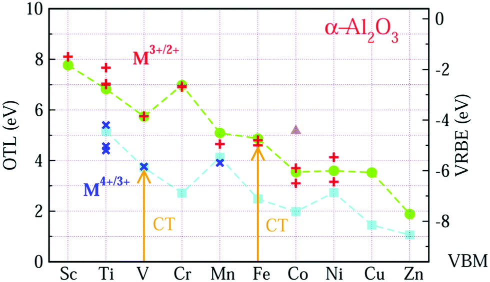 | ||
| Fig. 1 The OTL and VRBE of M ions in α-Al2O3. The circle and square symbols represent the OTL of εf(M3+/2+) and εf(M4+/3+), respectively. The plus and cross symbols represent experimental acceptor levels of M3+ and M4+ in α-Al2O3. The triangle is the OTL εf(Co3+/2+) with a low-spin state (see below). The arrows indicate the CT process. | ||
In Fig. 1, the data from the OTL of εf(M3+/2+) and εf(M4+/3+) are represented by circle and square symbols, respectively, while the data for the experimental acceptor levels of M3+ and M4+ are denoted as plus (+) and cross (×) symbols. In order to compare the OTL data of εf(M3+/2+) with the experimental data, the calculated results have been shifted upwards by about 0.77 eV. Although this calculation systematically underestimates the experimental values, the GGA-PBE calculation can work well in predicting the trend of the CT energies of the 3d-TM ions from Sc to Zn.
For OTL εf(M3+/2+) (the upper curve in Fig. 1), we find that except for Cr, the OTL decreases with the increase of the atomic number from Sc to Zn. This result is reasonable, since OTL is related to the defect levels, which may be inherited from the 3d orbitals of 3d-TM atoms. Like the 3rd ionization potentials of the free TM atoms, the binding energy of the 3d electron in 3d-TM atoms decreases with the growing number of nuclear charge. For Cr3+/2+, the OTL is about 1.2 eV higher than that of V3+/2+. As shown in Fig. S4 in the ESI,† V3+ has two valence electrons in the spin-up low triplet states. The OTL εf(V3+/2+) describes the energy needed to transfer an electron from VBM to V3+ ion. This electron should be accommodated in the spin-up low triplet states. However, Cr3+ (Fig. S5, ESI†) has three valence electrons that already fully occupy the spin-up low triplet states, and so the electron from the VBM has to occupy either the spin-up high doublet states or the spin-down triplet states (the OTL in these two cases are different by 0.043 eV). Obviously, this needs much more energy than in the case of V3+. This is why εf(Cr3+/2+) is about 1.2 eV larger than that of εf(V3+/2+).
The good agreement of OTL εf(M3+/2+) with the experimental CT band energies ECT(M,3) of trivalent TMs gives us the confidence that the CT band energies ECT(M,4) of tetravalent TM ions can also be predicted by the GGA-PBE calculations. From the experimental side, we only found CT data for Ti4+, V4+ and Mn4+ in Al2O3. The OTL εf(M4+/3+) curve reproduces those CT data, if it is lifted by 1.566 eV. The overall trend is that the εf(M4+/3+) decreases from Ti to Zn. The εf(Mn4+/3+) is more than 1 eV larger than εf(Cr4+/3+). The Mn4+ ion is like Cr3+ with three valence electrons, and the added electron has to occupy the higher energy doublet state. Also εf(Ni4+/3+) is higher than that of its neighbors. This can also be explained from the filling of the 3d-orbitals. As shown in Fig. S9 (ESI†), the Ni4+ ion has six valence electrons which fully occupy the low triplet states with both spin-up and spin-down. The added electron has to occupy the higher energy doublet states.
Comparing the two OTL curves, one observes that when the lower curve is shifted leftwards by one element these two curves run nearly parallel, except for the data points of εf(Ni4+/3+) and εf(Co3+/2+). The reason is that similar 3dn configurations are now compared. For two M ions with the same electron configuration, the value for the lower curve is about 2.5 eV lower than that for the upper curve. This difference is a direct consequence of the higher ionic charge. Although both Ni4+ and Co3+ have six valence electrons, their electronic configurations are different. As shown in Fig. S8 and S9 in ESI,† five valence electrons of Co3+ occupy the spin-up states with one valence electron located at the low spin-down triplet states, resulting in a local magnetic moment of 4 μB at Co3+. This state is consistent with the experimental ground state of t4e2.23 We denote this state as the high-spin state. For Ni4+, six valence electrons occupy the lower triplet states with both spin orientations, and thus the local magnetic moment of Ni4+ is 0 μB. So this state is labeled as the low-spin state. The OTL of Co3+ in the low-spin state has also been calculated, which is about 1.626 eV higher than that of the high-spin state as shown in Fig. 1 (the triangle).
Considering the similarity of OTL εf(Mn+/(n−1)+) and CT band energies ECT(M,n), the VRBE E(M,n − 1) is also computed from the OTL εf(Mn+/(n−1)+). The results are shown in Fig. 1 with the right side y-axis. By connecting these OTL or VRBE values, we obtain the zig-zag like curves of OTL (VRBE) of the M ions in α-Al2O3.
Fig. 2 shows the VRBE curves of 3d-TM ions in YAG by using the experimental data listed in Table 1 and first-principles calculations. All the electronic structures are shown in ESI.† In Fig. 2, the OTL of εf(M3+/2+) and εf(M4+/3+) in YAG are represented by circle and square symbols, respectively, while the corresponding experimental acceptor levels are denoted as plus (+) and cross symbols (×). The VRBE is shown in Fig. 2 on the right side y-axis. The resulting εf(Sc3+/2+), εf(Ti3+/2+) and εf(Cr3+/2+) are inaccurate and the reason is discussed in part C of the ESI.† In Fig. 2, we adopt open symbols to distinguish εf(Sc3+/2+), εf(Ti3+/2+) and εf(Cr3+/2+) from other OTLs. For the upper curve, the energy difference between the OTL of εf(Fe3+/2+) and εf(Ni3+/2+) agrees well with the experiments after the calculated OTL are shifted upwards by 0.656 eV. For more evidence, we also calculate the OTL of Fe ions in tetrahedral site and the difference of εf(Fe3+/2+) at tetrahedral and octahedral sites is only −0.14 eV, while the CT of Fe ions in these two sites is experimentally the same.40 For the lower curve, the calculated results are shifted upwards by 1.357 eV.
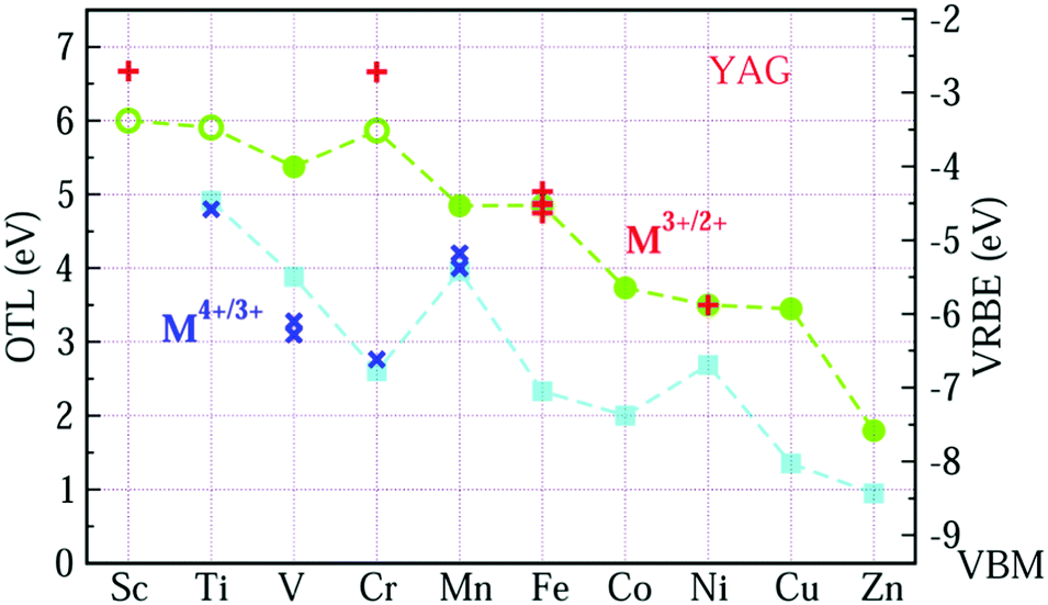 | ||
| Fig. 2 The OTL and VRBE of M ions in YAG. The circle and square symbols represent OTL of εf(M3+/2+) and εf(M4+/3+), respectively, where the open and full symbols denote the accurate and inaccurate results. The plus and cross symbols represent acceptor levels of 3d-TM ions with 3+ and 4+ in YAG extracted from the CT data. Note, the coordination of V4+/3+ is not specified in the literature. | ||
Comparing Fig. 2 with Fig. 1, we find that the VRBE curves are very similar to each other. So, we replot these VRBE curves in Fig. 3 for comparison. Here, the VRBE of εf(M3+/2+) and εf(M4+/3+) in α-Al2O3 is represented by the circle and square symbols, while in YAG by up and down triangles. The VRBE curves of M in both YAG and α-Al2O3 are almost parallel, respectively, except the underestimated values for Sc3+/2+, Ti3+/2+ and Cr3+/2+ in YAG.
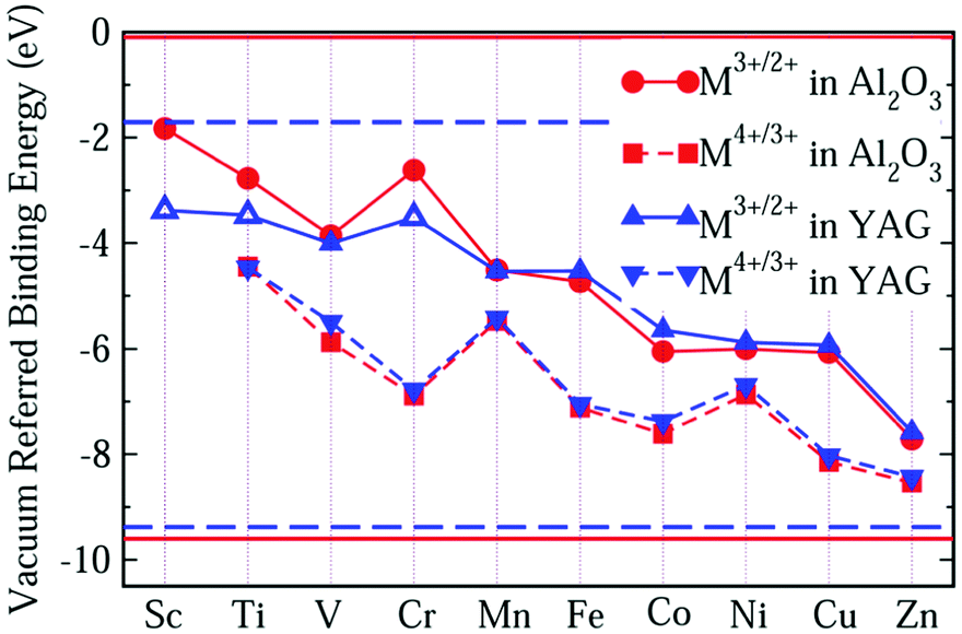 | ||
| Fig. 3 The VRBE of M ions in α-Al2O3 and YAG. The circle and square symbols represent VRBE of εf(M3+/2+) and εf(M4+/3+) in α-Al2O3, while the up and down triangle represent VRBE of εf(M3+/2+) and εf(M4+/3+) in YAG. The horizontal lines represent experimental VBM (lower) and conduction band minimum (upper) of Al2O3 (solid line) and YAG (dash line). | ||
The similarity in the VRBE curves of α-Al2O3 and YAG can be understood from molecular orbital theory. As shown in Fig. 4, the 3d orbitals of the M ion couple with the ligand bonds. The ligand bonds are fully occupied and are from the bonding orbitals of O ions and cations, such as Al3+ in α-Al2O3 or Y3+ and Al3+ in YAG. The combination of the ligand bonds with dx2−y2 or dz2 orbital forms a σ bonding orbital with the lowest energy (denoted as e) and σ antibonding orbital (e*) with the highest energy. Between these orbitals are t and t*, which are π bonding and antibonding orbitals originating from the coupling of dxy, dxz or dyz with the ligand bonds. The e and t orbitals are lower in energy than the ligand bonds and are fully occupied by the electrons from the ligand bonds. (Theoretically, the electrons are indistinguishable, but we notionally indicate the electrons as being derived from the ligands or 3d-TM for the purpose of filling the energy-level diagram.) The t* and e* orbitals have higher energies, and appear in the band gap as defect levels. The 3d-electrons from the M ion will go to fill the t* and e* orbitals. So the energies of t* or e* dominate 3d-TM VRBE. As we limited M ions to the octahedral site, the factors that affect VRBE are the size of AlO6 and the energies of ligand bonds. The average Al–O bond length is 191.5 pm in α-Al2O3 and 192 pm for the octahedral Al site in YAG. The ligand bonds in the crystal form the VB. As shown in Fig. S1 in the ESI,† the VB of both compounds have a width of about 7 eV with the VBM at about −9.6 eV for α-Al2O3 and −9.38 eV for YAG (here the reference energy is the vacuum level). Thus, the defect levels of M ions in these two compounds are similar to each other and then also to the VRBE of 3d-TM.
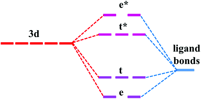 | ||
| Fig. 4 Schematic energy level diagram for transition metal in the octahedral site of α-Al2O3 and YAG. Not drawn to scale. | ||
As shown in Fig. 5(a), the Al–O bonds in α-Al2O3 are about 186 pm and 197 pm (calculated result) with O–Al–O angles of about 79.71°, 90.736°, and 101.17°, which have large deviations from the perfect Al–O octahedron. For the octahedron in YAG, the O–Al–O angles are 93.20° and 86.80° (Fig. 5(b)) and close to perfect. However, the VRBE of 3d-TM in these two compounds is very similar. These results imply that the distortion of crystal field has little influence on the VRBE.
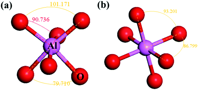 | ||
| Fig. 5 The Al–O octahedron in (a) α-Al2O3 and (b) YAG with different crystal field distortions. The data present the angle of adjacent O–Al bonding. | ||
Although the VRBE curve of 3d-TMs in YAG is similar to that in α-Al2O3, they are not exactly the same as seen in Fig. 3. The question then arises how to predict the VRBE of 3d-TMs in other aluminates with octahedral sites. Considering the relatively scarce CT data of 3d-TM in a specific aluminate, it is difficult to obtain a complete VRBE curve similar to α-Al2O3 and YAG. Yet, to obtain the VRBE of a given 3d-TM ion at an octahedral site in different aluminates seems to be feasible. Rogers and Dorenbos reported that the VRBEs of Ti4+/3+ in many different oxides fall within ±1 eV from the mean value of −3.95 eV.49 For Mn4+, Fe3+ and Cr3+ oxides, we collected in Table 2 the CT band energies, and the corresponding VRBEs for Mn4+/3+, Fe3+/2+ and Cr3+/2+ are shown in Fig. 6. For Mn4+/3+, the compounds covered include aluminates plus the zirconate CaZrO3. The average acceptor VRBE value is −4.82 eV with a spread of ±0.8 eV. Since the O2−–Mn4+ CT band is very broad and there is often a strong overlap between the 4A2g → 4T1g band and the CT band, it is difficult to determine the precise CT peak position.
| Ions | Host | E CT | E V | E C | VRBE |
|---|---|---|---|---|---|
| a Here, the bandgap of MgO at room temperature is about 7.6 eV74 and the Ev can be deduced from the data in the literature.75 Its impurity level is about 0.8 eV below the conduction band of MgO.76 So the VRBE of Cr3+ in MgO would be about −2.02 eV. Its CT value is about 6.8 eV, which is also listed in the table for completeness. b See the experimental data in ESI. c This value is obtained from TL results.16 | |||||
| Mn4+ | LaAlO3 | 3.69,53 3.5454 | −7.83 | −1.45 | −4.14, −4.29 |
| GdAlO3 | 3.8055 | −8.66 | −0.67 | −4.86 | |
| SrAl12O19 | 3.6956 | −8.23 | −0.30 | −4.54 | |
| CaAl12O19 | 3.6757 | −8.13 | −0.40 | −4.46 | |
| YAlO3 | 4.1358 | −9.04 | −0.44 | −4.91 | |
| SrMgAl10O17 | 3.8459 | −8.63 | −2.43 | −4.79 | |
| Y3Al5O12 | 4.20,36 4.037 | −9.38 | −1.71 | −5.18, −5.38 | |
| Sr4A114O25 | 3.7960 | −8.03 | −0.74 | −4.24 | |
| α-LiAlO2 | 3.8861 | −8.88 | −0.4 | −5.00 | |
| CaYAlO4 | 3.7062 | −8.56 | −2.32 | −4.86 | |
| SrAl4O7 | 3.8163 | −8.41 | −1.93 | −4.60 | |
| α-Al2O3 | 3.9135 | −9.60 | −0.08 | −5.69 | |
| CaZrO3 | 3.2564 | −8.35 | −2.46 | −5.10 | |
| Fe3+ | LiAl5O8 | 4.3565 | −8.6 | 0.4 | −4.25 |
| Y3Al5O12 | 4.86,40 4.88,41 5.04,42 4.7542 | −9.38 | −1.71 | −4.52, −4.50, −4.34, −4.63 | |
| Y3Ga5O12 | 4.6466 | −9.01 | −2.42 | −4.37 | |
| α-Al2O3 | 4.80,22,38 4.6039 | −9.60 | −0.08 | −4.8, −5.0 | |
| MgO | 4.27,67 4.30,68 4.43,69 4.0269 | −8.60 | −0.80 | −4.33, −4.30, −4.17, −4.58 | |
| α-Ga2O3 | 3.5970 | −8.17 | −3.63 | −4.58 | |
| GdAlO3 | 4.20b | −8.66 | −0.67 | −4.30 | |
| BaTiO3 | 2.371 | −7.25 | −3.59 | −4.95 | |
| Cr3+ | α-Al2O3 | 6.94,22 6.9033 | −9.6 | −0.08 | −2.66, −2.70 |
| β-Ga2O3 | 4.1050 | −8.17 | −3.63 | −4.07 | |
| ZnGa2O4 | 4.5651 | −8.40 | −3.50 | −3.84 | |
| Y3Al5O12 | 6.66c | −9.38 | −1.71 | −2.72c | |
| MgOa | 6.80 | −8.82 | −1.22 | −2.02 | |
| LaAlO3 | 5.2872 | −7.82 | −1.22 | −2.54 | |
| GdAlO3 | 6.3673 | −8.66 | −0.92 | −2.30 | |
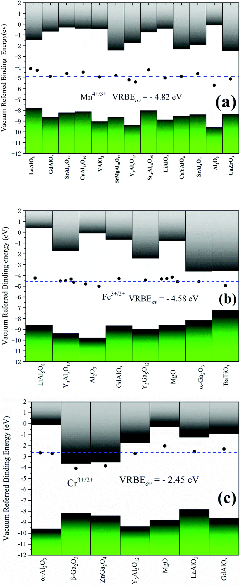 | ||
| Fig. 6 Stacked VRBE schemes for acceptor levels of Mn4+/3+, Fe3+/2+ and Cr3+/2+ in different phosphors. The valence and conduction bands are represented by the bottom and top bars, respectively. The solid data point is the VRBE of those acceptor levels in a specific compound. Horizontal dashed line denotes the average VRBE for those acceptor levels. | ||
Fig. 6(b) shows that the average VRBE of Fe3+/2+ is −4.50 eV in aluminates with a spread ±0.4 eV. We also collected the VRBEs of Fe3+/2+ in other oxides, like Y3Ga5O12, MgO, α-Ga2O3 and the titanate BaTiO3, and find that those values are quite well consistent with that average value. We take the average value (−4.58 eV) covering all the Fe3+-doped oxides listed in Table 2 as the VRBE of Fe3+/2+ with a spread of about ±0.4 eV.
The VRBE of Cr3+/2+ locates at about −2.45 eV with a range of ±0.3 eV, as shown in Fig. 6(c). This value does not cover β-Ga2O3 and ZnGa2O4, since the acceptor level of Cr3+ is very close to their conduction bands. So, it is difficult to distinguish the CT bands of Cr3+ from the host absorption. In the literature,50,51 the host band absorptions of β-Ga2O3 and ZnGa2O4 were regarded as the CT bands as shown in Fig. 6(c). In these cases, the actual VRBE value could be largely underestimated. A similar situation may occur for Sc3+-doped compounds.14
Although the VRBEs of Ti4+/3+, Mn4+/3+, Cr3+/2+ and Fe3+/2+ in the listed compounds show a spread of about ±1 eV, their mean values still can offer a first estimate on the location of TM acceptor levels in compounds. For the average VRBEs of other 3d-TM ions, we could not obtain enough CT data to extract them. An alternative approach is to shift our OTL curves until the VRBEs of Fe3+/2+ and Mn4+/3+ evaluated from our calculation are consistent with the average values in Fig. 6(a and b), respectively. The results are shown in Fig. 7 and Table 3. The VRBEs of Ti4+/3+ and Cr3+/2+ predicted from our VRBE curves are about −3.792 eV and −2.468 eV, and the corresponding experimental mean values are about −3.95 eV49 and −2.49 eV. The VRBEs of Cr3+ impurity levels in GdAlO3 and LaAlO3 obtained through the Cr3+-CB electron transfer process are about −6.2 ± 0.2 eV and −6.3 ± 0.2 eV, respectively,73 which are also very close to our Cr4+/3+ data of −6.235 eV. Such good agreement demonstrates that our VRBE curves in Fig. 7 also fit well with other 3d-TM ions in octahedral aluminates. Thus, the VRBE curves in Fig. 6 can be used to roughly predict the acceptor levels of 3d-TM ions at octahedral sites in a given aluminate.
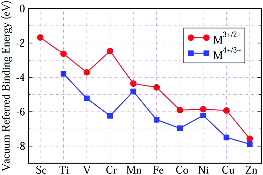 | ||
| Fig. 7 The average VRBE of 3d-TM ions in aluminates predicted by combining the calculated OTL energies with the experimental CT-energies. | ||
| TM3+/2+ | TM4+/3+ | |
|---|---|---|
| Sc | −1.679 | — |
| Ti | −2.626 | −3.792 |
| V | −3.709 | −5.221 |
| Cr | −2.468 | −6.235 |
| Mn | −4.360 | −4.820 |
| Fe | −4.580 | −6.464 |
| Co | −5.904 | −6.962 |
| Ni | −5.853 | −6.214 |
| Cu | −5.924 | −7.494 |
| Zn | −7.566 | −7.885 |
In an attempt to arrive at a more accurate prediction of VRBE, we studied the fluctuation of the 3d-TM VRBE in different aluminates. The dashed line in Fig. 8 shows that when the VRBE at the VBM increases, the VRBE of the Mn4+/3+ acceptor level increases linearly with a slope of about 0.74. The maximum deviation of the experimental VRBE of Mn4+/3+ from the dashed line is 0.19 eV. So, the estimation of the VRBE of Mn4+/3+ in an aluminate might be more accurately made if the VRBE of the VBM is known.
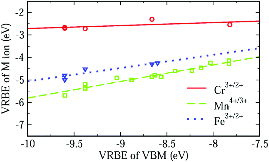 | ||
| Fig. 8 The VRBE of Cr3+/2+, Fe3+/2+ and Mn4+/3+ as a function of the VBM of different aluminates with octahedral sites derived from Table 2. | ||
The relationship between the VRBE of Mn4+/3+ and VBM could be understood from molecular orbital theory. As mentioned above, the VRBE of the Mn ion is dominated by the antibonding orbitals t* and e*. On raising the energies of ligand bonds, the t* and e* orbitals increase in energy and so does the VRBE of the Mn ion. Since the VB is mainly formed by ligand bonds, the increase of the energies of ligand bonds can cause the VBM to shift upwards. So, the VRBE of Mn4+/3+ increases with the increase of VBM. This rule can also be applied for the VRBEs of other 3d-TM ions. So, we fitted the VRBE of Cr3+/2+ or Fe3+/2+ to a straight line as shown by the solid or dotted line in Fig. 8. Their slopes are about 0.13 and 0.59 with the largest data deviations of about 0.23 eV and 0.18 eV, respectively. When more data are available these seemingly linear relationships can be tested further. Here we used the VBM as a variable but other aspects like the crystal field splitting of the 3dn level can also be important.
Finally, we will elaborate somewhat further on the charge states of the M ions in compounds. When the energies of the 3d orbitals are higher than those of the ligand bonds, t* and e* are mainly contributed by the 3d orbitals. Sc, Ti, V, Cr, Mn, Fe and Co ions belong to this category, which can be proved by the PDOS in Fig. S2–S8 of the ESI.† So, the electrons in the t* and e* can be roughly regarded as the 3d electrons of the M ions. The OTL and CT energies then reflect the location of the acceptor levels induced by the t* or e* orbitals and thus approximately reflect the VRBE of the 3d orbitals of M ions. So, we denote them, for example, as OTL(M3+/2+) or ECT(M,3). When the atomic number increases from Sc to Zn, the energies in the 3d orbitals decrease and the contribution of ligand bonds (which are mostly O 2p orbitals) to the t* or e* orbitals increases. Especially, in the case of Zn, the defect levels are mostly contributed by O 2p orbitals, while the contribution of 3d orbitals concentrates on the bonding t and e orbitals, which are about 3–6.0 eV below the VBM. Now, the electrons in the t* and e* should be roughly regarded as the p electrons of O ions. Thus, the charge state of the Zn ion is nearly unrelated to the defect levels in the band gap. In other words, the Zn ion should be approximately in the 2+ state in all the calculations, as two 4s electrons of Zn atom are delocalized when doped. However, the OTL and CT energies still reflect the locations of acceptor levels induced by t* or e* orbitals. Although the contribution of the 3d orbitals of Zn to the t* and e* orbitals is negligibly small, the energies of 3d orbitals still can be considered as part of the e* orbitals. So, we adopted OTL(Zn3+/2+) or ECT(Zn,3) to denote the corresponding OTL or CT bands, nominally.
Conclusion
In this work, we offer a method to predict the acceptor levels of 3d-TM ions in octahedral aluminates by constructing zig-zag like VRBE curves employing the experimental CT band energies of 3d-TM ions and by first-principles calculation. These curves offer a rough estimate about the acceptor level energies of 3d-TM ions with a spread of about ±1 eV. The estimation can be more accurate if we take the molecular orbital theory into consideration without complicated calculations. Our work gives a vivid and quantitative explanation of how binding energy varies with the increase of n for the 3d orbital electrons, and makes it easier to estimate their doping levels in a specific compound. Those predictable levels are very useful in engineering the luminescent properties of 3d-TM activated phosphors. For the phosphors with tetrahedral sites, such as silicates, (oxy)nitrides, we speculate that similar rules may exist from the view of the molecular orbital theory, but the shape of the zig-zag-curve should be different from that in octahedral sites as shown in Fig. 7. We need more experimental data to extract and verify them. This work is under way.Conflicts of interest
There are no conflicts to declare.Acknowledgements
This work was supported by the National Natural Science Foundation of China (Grant No: 51302059 and 11404085), NSAF (Grant No: U1630118), China Scholarship Council (201406695020) and the Natural Science Foundation of Anhui Province (Grant 1708085ME121). Calculations were carried out at the Supercomputing Center of University of Science and Technology of China.References
- S. Kück, Appl. Phys. B: Lasers Opt., 2001, 72, 515–562 CrossRef.
- Y. Hao and Y. Wang, J. Lumin., 2007, 122–123, 1006–1008 CrossRef CAS.
- W. Lü, W. Lv, Q. Zhao, M. Jiao, B. Shao and H. You, Inorg. Chem., 2014, 53, 11985–11990 CrossRef PubMed.
- H.-D. Nguyen, C. C. Lin, M.-H. Fang and R.-S. Liu, J. Mater. Chem. C, 2014, 2, 10268–10272 RSC.
- L. Wang, Z. Dai, R. Zhou, B. Qu and X. C. Zeng, Phys. Chem. Chem. Phys., 2018, 20, 16992–16999 RSC.
- Z. Pan, Y.-Y. Lu and F. Liu, Nat. Mater., 2012, 11, 58–63 CrossRef CAS PubMed.
- Y. Wang and L. Wang, J. Appl. Phys., 2007, 101, 053108 CrossRef.
- Z. Liu, L. Zhao, W. Chen, S. Xin, X. Fan, W. Bian, X. Yu, J. Qiu and X. Xu, J. Am. Ceram. Soc., 2018, 101, 3480–3488 CrossRef CAS.
- B. Qu, B. Zhang, L. Wang, R. Zhou and X. C. Zeng, Chem. Mater., 2015, 27, 2195–2202 CrossRef CAS.
- G. Blasse and B. Grabmaier, Luminescent materials, Springer, Berlin, 1994 Search PubMed.
- B. Qu, B. Zhang, L. Wang, R. Zhou, X. C. Zeng and L. Li, ACS Appl. Mater. Interfaces, 2016, 8, 5439–5444 CrossRef CAS PubMed.
- P. Dorenbos, Phys. Rev. B: Condens. Matter Mater. Phys., 2012, 85, 165107 CrossRef.
- P. Dorenbos, Phys. Rev. B: Condens. Matter Mater. Phys., 2013, 87, 035118 CrossRef.
- E. G. Rogers and P. Dorenbos, ECS J. Solid State Sci. Technol., 2014, 3, R173–R184 CrossRef CAS.
- J. Ueda, A. Hashimoto, S. Takemura, K. Ogasawara, P. Dorenbos and S. Tanabe, J. Lumin., 2017, 192, 371–375 CrossRef CAS.
- J. Ueda, P. Dorenbos, A. J. J. Bos, K. Kuroishi and S. Tanabe, J. Mater. Chem. C, 2015, 3, 5642–5651 RSC.
- P. Dorenbos, Opt. Mater., 2017, 69, 8–22 CrossRef CAS.
- G. Kresse and J. Furthmüller, Phys. Rev. B: Condens. Matter Mater. Phys., 1996, 54, 11169–11186 CrossRef CAS.
- G. Kresse and J. Hafner, Phys. Rev. B: Condens. Matter Mater. Phys., 1993, 47, 558–561 CrossRef CAS.
- J. P. Perdew, K. Burke and M. Ernzerhof, Phys. Rev. Lett., 1996, 77, 3865–3868 CrossRef CAS PubMed.
- C. G. V. d. Walle and J. Neugebauer, J. Appl. Phys., 2004, 95, 3851–3879 CrossRef.
- H. H. Tippins, Phys. Rev. B: Condens. Matter Mater. Phys., 1970, 1, 126–135 CrossRef CAS.
- D. S. McClure, J. Chem. Phys., 1962, 36, 2757–2779 CrossRef CAS.
- M. Kirm, G. Zimmerer, E. Feldbach, A. Lushchik, C. Lushchik and F. Savikhin, Phys. Rev. B: Condens. Matter Mater. Phys., 1999, 60, 502–510 CrossRef CAS.
- V. Mürk and N. Yaroshevich, Phys. Status Solidi B, 1994, 181, K37–K40 CrossRef.
- Y. Zorenko, T. Zorenko, T. Voznyak, S. Nizhankovskiy, E. Krivonosov, A. Danko and V. Puzikov, Opt. Mater., 2013, 35, 2053–2055 CrossRef CAS.
- W. C. Wong, D. S. McClure, S. A. Basun and M. R. Kokta, Phys. Rev. B: Condens. Matter Mater. Phys., 1995, 51, 5682–5692 CrossRef CAS.
- M. Yamaga, T. Yosida, S. Hara, N. Kodama and B. Henderson, J. Appl. Phys., 1994, 75, 1111–1117 CrossRef CAS.
- G. Molnár, M. Benabdesselam, J. Borossay, D. Lapraz, P. Iacconi, V. S. Kortov and A. I. Surdo, Radiat. Meas., 2001, 33, 663–667 CrossRef.
- T. Huang, B. Jiang, Y. Wu, J. Li, Y. Shi, W. Liu, Y. Pan and J. Guo, J. Alloys Compd., 2009, 478, L16–L20 CrossRef CAS.
- J. P. Meyn, T. Danger, K. Petermann and G. Huber, J. Lumin., 1993, 55, 55–62 CrossRef CAS.
- M. J. Weber and L. A. Riseberg, J. Chem. Phys., 1971, 55, 2032–2038 CrossRef CAS.
- V. A. Pustovarov, V. S. Kortov, S. V. Zvonarev and A. I. Medvedev, J. Lumin., 2012, 132, 2868–2873 CrossRef CAS.
- S. Kück, K. Petermann, U. Pohlmann and G. Huber, J. Lumin., 1996, 68, 1–14 CrossRef.
- Y. Xu, L. Wang, B. Qu, D. Li, J. Lu and R. Zhou, J. Am. Ceram. Soc., 2018 DOI:10.1111/JACE.16155.
- K. Petermann and G. Huber, J. Lumin., 1984, 31–32(Part 1), 71–77 CrossRef CAS.
- D. Q. Chen, Y. Zhou, W. Xu, J. S. Zhong, Z. G. Ji and W. D. Xiang, J. Mater. Chem. C, 2016, 4, 1704–1712 RSC.
- J. B. Blum, H. L. Tuller and R. L. Coble, J. Am. Ceram. Soc., 1982, 65, 379–382 CrossRef CAS.
- R. Moncorge, G. Boulon, D. Vivien, A. M. Lejus, R. Collongues, V. Djevahirdjian, K. Djevahirdjian and R. Gagnard, IEEE J. Quantum Electron., 1988, 24, 1049–1051 CAS.
- C. Y. Chen, G. J. Pogatshnik, Y. Chen and M. R. Kokta, Phys. Rev. B: Condens. Matter Mater. Phys., 1988, 38, 8555–8561 CrossRef CAS.
- K. Mori, Phys. Status Solidi A, 1977, 42, 375–384 CrossRef CAS.
- I. S. Akhmadullin, S. A. Migachev and S. P. Mironov, Nucl. Instrum. Methods Phys. Res., Sect. B, 1992, 65, 270–274 CrossRef.
- S. R. Rotman, M. Roth, H. L. Tuller and C. Warde, J. Appl. Phys., 1989, 66, 1366–1369 CrossRef CAS.
- S. R. Rotman and H. L. Tuller, J. Appl. Phys., 1987, 62, 1305–1312 CrossRef CAS.
- N. Manuilov and P. Peshev, Mater. Res. Bull., 1989, 24, 1549–1555 CrossRef CAS.
- M. Yamaga, Y. Oda, H. Uno, K. Hasegawa, H. Ito and S. Mizuno, J. Appl. Phys., 2012, 112, 063508 CrossRef.
- P. Hong, X. X. Zhang, C. W. Struck and B. D. Bartolo, J. Appl. Phys., 1995, 78, 4659–4667 CrossRef CAS.
- P. Dorenbos, J. Lumin., 2013, 134, 310–318 CrossRef CAS.
- E. G. Rogers and P. Dorenbos, J. Lumin., 2014, 153, 40–45 CrossRef CAS.
- H. Wakai, Y. Sinya and A. Yamanaka, Phys. Status Solidi C, 2011, 8, 537–539 CrossRef CAS.
- A. Bessière, S. K. Sharma, N. Basavaraju, K. R. Priolkar, L. Binet, B. Viana, A. J. J. Bos, T. Maldiney, C. Richard, D. Scherman and D. Gourier, Chem. Mater., 2014, 26, 1365–1373 CrossRef.
- E. G. Rogers and P. Dorenbos, J. Lumin., 2014, 155, 135–140 CrossRef CAS.
- Y. Li, Y.-Y. Li, K. Sharafudeen, G.-P. Dong, S.-F. Zhou, Z.-J. Ma, M.-Y. Peng and J.-R. Qiu, J. Mater. Chem. C, 2014, 2, 2019–2027 RSC.
- M. E. van Ipenburg, G. J. Dirksen and G. Blasse, Mater. Chem. Phys., 1995, 39, 236–238 CrossRef CAS.
- A. M. Srivastava and M. G. Brik, Opt. Mater., 2017, 63, 207–212 CrossRef CAS.
- L. Wang, Y. Xu, D. Wang, R. Zhou, N. Ding, M. Shi, Y. Chen, Y. Jiang and Y. Wang, Phys. Status Solidi A, 2013, 210, 1433–1437 CrossRef CAS.
- T. Murata, T. Tanoue, M. Iwasaki, K. Morinaga and T. Hase, J. Lumin., 2005, 114, 207–212 CrossRef CAS.
- M. A. Noginov and G. B. Loutts, J. Opt. Soc. Am. B, 1999, 16, 3–11 CrossRef CAS.
- R. Cao, K. N. Sharafudeen and J. Qiu, Spectrochim. Acta, Part A, 2014, 117, 402–405 CrossRef CAS PubMed.
- M. Peng, X. Yin, P. A. Tanner, C. Liang, P. Li, Q. Zhang and J. Qiu, J. Am. Ceram. Soc., 2013, 96, 2870–2876 CrossRef CAS.
- M. Aoyama, Y. Amano, K. Inoue, S. Honda, S. Hashimoto and Y. Iwamoto, J. Lumin., 2013, 136, 411–414 CrossRef CAS.
- Y. Chen, M. Wang, J. Wang, M. Wu and C. Wang, J. Solid State Light., 2014, 1, 15 CrossRef.
- R. Cao, Q. Xiong, W. Luo, D. Wu, X. Fen and X. Yu, Ceram. Int., 2015, 41, 7191–7196 CrossRef CAS.
- G. Blasse and P. H. M. D. Korte, J. Inorg. Nucl. Chem., 1981, 43, 1505–1506 CrossRef CAS.
- T. R. N. Kutty and M. Nayak, J. Alloys Compd., 1998, 269, 75–87 CrossRef CAS.
- D. E. Lacklison, G. B. Scott and J. L. Page, Solid State Commun., 1974, 14, 861–863 CrossRef CAS.
- S. Clement and E. R. Hodgson, Mrs Online Proceeding Library, 2011, 60.
- A. M. Stoneham, M. J. L. Sangster and P. W. Tasker, Philos. Mag. B, 1981, 44, 603–613 CAS.
- K. Dunphy and W. W. Duley, J. Phys. Chem. Solids, 1990, 51, 1077–1082 CrossRef CAS.
- G. T. Pott and B. D. McNicol, J. Lumin., 1973, 6, 225–228 CrossRef CAS.
- A. Mazur, C. Veber, O. F. Schirmer, C. Kuper and H. Hesse, Radiat. Eff. Defects Solids, 1999, 150, 281–286 CrossRef.
- Y. Katayama, H. Kobayashi and S. Tanabe, Appl. Phys. Express, 2015, 8, 012102 CrossRef.
- H. Luo and P. Dorenbos, J. Mater. Chem. C, 2018, 6, 4977–4984 RSC.
- M. L. Bortz, R. H. French, D. J. Jones, R. V. Kasowski and F. S. Ohuchi, Phys. Scr., 1990, 41, 537 CrossRef CAS.
- P. Dorenbos, J. Lumin., 2005, 111, 89–104 CrossRef CAS.
- C. C. Chao, J. Phys. Chem. Solids, 1971, 32, 2517–2528 CrossRef CAS.
Footnote |
| † Electronic supplementary information (ESI) available. See DOI: 10.1039/c8tc05401k |
| This journal is © The Royal Society of Chemistry 2019 |