DOI:
10.1039/D0MA00603C
(Paper)
Mater. Adv., 2020,
1, 3322-3332
Significant enhancement of the thermoelectric properties of CaP3 through reducing the dimensionality†
Received
14th August 2020
, Accepted 25th October 2020
First published on 26th October 2020
Abstract
Through first-principles calculations and using the Boltzmann transport equation, we explore the thermoelectric (TE) properties of CaP3 from the three-dimensional (3D) bulk form to a two-dimensional (2D) monolayer. Herein, our results prove that reducing the dimensionality not only can avoid the poor TE performance along certain crystal orientations, but also can effectively reduce the thermal conductivity. More remarkably, the Seebeck coefficients of the monolayer exhibit a dramatic enhancement compared to its bulk form. Some inherent phonon properties, such as the low acoustic phonon group velocity of ∼1.41 km s−1, large Grüneisen parameters of ∼30, and short phonon relaxation time, can greatly hinder its heat transport ability, leading to an ultralow lattice thermal conductivity of ∼0.65 W m−1 K−1 for the monolayer at room temperature. The size effect is much less sensitive due to the short intrinsic phonon mean free path (MFP). The maximum figure of merit (ZT) for n-type doping at 700 K can reach 6.39 in the nanosheet along the a direction, which is enhanced nearly two times compared to its bulk form (2.83), due to the quantum confinement effect. Collectively, this work shows that low-dimensional nanostructure technology can effectively improve the thermoelectric conversion of this class of materials.
1 Introduction
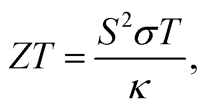
TE materials have attracted much attention because they can be used to directly convert waste heat into electrical energy (the Seebeck effect) and vice versa (the Peltier effect).1–3 Usually, the efficiency of TE energy generators is relatively low (<10%) and it can be determined by the dimensionless figure of merit,4,5| |  | (1) |
in which S, T, and σ are the Seebeck coefficient, absolute temperature, and electric conductivity, respectively, and κ is the total thermal conductivity composed of the phononic (κl) and electronic (κe) contributions. Normally, a low κ and/or large power factor S2σ are required for designing highly efficient TE devices.6 However, optimizing simultaneously these transport parameters is an arduous process due to the complex competition among them, which greatly limits the TE performance of materials.7 In the past few years, in order to regulate and control these complex parameters, band structure engineering8,9 and the quantum confinement effect10 have been used to optimize electric transport coefficients, while other effects are presented to reduce κl through phononic crystal patterning11,12 or dimensionality reduction.13 Generally, inherent low κl is a crucial precondition for achieving high TE performance, because it can maintain in a fixed range when optimizing the electrical coefficients. Therefore, searching for new materials with low κl is of great significance for fast-paced development of TE applications.
2D layered materials, such as single layer graphene,16–18 silicene,19,20 phosphorene,21,22 borophene,23,24 and a series of other layered materials,25–27 have been systematically investigated in the scientific community for use as TE materials. Recently, 2D triphosphides have been reported one after another with fascinating properties, attracting great attention.28,29 For instance, the GeP3 and SnP3 nanosheets exhibit tunable band gaps and strong interlayer quantum confinement effects.30,31 Additionally, it is reported that GaP3 and SbP3 possess high carrier mobility and large optical absorption coefficients (>105 cm−1) in the visible and ultraviolet regions.32 In particular, the InP3 monolayer with a plicated configuration shows an ultralow thermal conductivity (∼0.63 W m−1 K−1 at 300 K) and a high electron mobility of 1919 cm2 V−1 s−1.33,34 With excellent phononic and electronic properties, the unexpectedly high ZT can reach 2.06 for p-type doping at room temperature. Therefore, the triphosphides, as important components of phosphorene derivatives, are hopeful alternatives for applications in microelectronic, photovoltaic and thermoelectric technologies.
Bulk CaP3, first synthesized in the 1970s,15 has been recently regarded as a topological nodal-line semimetal.35 It has been predicted by Lu et al. that a CaP3 nano-thin film, due to its bulk form possessing a layered structure, could be mechanically cleaved from its bulk phase.14 Similar to their bulk form, monolayer and multilayer CaP3 are also direct band gap semiconductors with the band gap strongly dependent on the number of stacked layers. Unlike the surface of the plicated configuration in common triphosphides,30 CaP3 nanosheets possess a unique cage structure and rough surface, which can enhance surface phonon scattering and suppress the heat transport ability. Besides its excellent electronic transport properties and characteristic crystal structure, it also exhibits other advantages of high thermostability (∼1000 K) and a large optical absorption coefficient (∼105 cm−1), opening its potential application in nanoelectronics and optoelectronics.14 In view of these physical properties, CaP3 may have surprising TE performance.
In our present work, we study the TE properties of CaP3 from the bulk to a monolayer by using the density-functional-theory (DFT) and Boltzmann transport methods. The results show that an enormous difference can be observed in the Seebeck coefficients between the two forms, mainly originating from their unique electronic band structures. It is gratifying to find that κl is greatly reduced from the bulk (2.14 W m−1 K−1) to the monolayer (0.65 W m−1 K−1) at room temperature. Detailed discussions of the phonon scattering, phonon group velocity, Grüneisen parameters, atomic vibrational modes, and phonon relaxation time are presented to help understand the difference in thermal conductivity between the two forms. Due to their short intrinsic phonon MFP, the size effect is much less sensitive. Combined with these available parameters, the unexpected high ZT value can approach 6.39 for the monolayer at 700 K, which is a very desirable value for TE generators. All these findings demonstrate that reducing the dimensionality could be an effective way to modulate the TE performance of layered materials.
2 Computational details
First-principles calculations of monolayer and bulk CaP3 were performed by utilizing the Vienna Ab initio Simulation Package (VASP).36 The generalized gradient approximation (GGA)37 in the Perdew–Burke–Ernzerhof (PBE)38 form for the exchange–correlation functional was adopted. The Ca 3p64s2 and the P 3s23p3 orbitals were treated as valence electrons. The kinetic energy cutoff was chosen as 500 eV for the plane-wave expansion of the electronic wave function and the Brillouin zone (BZ) was sampled with 9 × 9 × 1 and 7 × 7 × 7 k-meshes for the unit cells of the monolayer and bulk, respectively. For the monolayer, the layer thickness was set as 20 Å along the z direction to eliminate the interaction between periodic layers. The van der Waals (vdW) interactions were corrected by using optB88-vdW.39 All geometric structures were fully relaxed until the forces on each atom were less than 0.001 eV Å−1. The energy convergence criterion was set as 10−6 eV Å−1. In order to obtain a more accurate electronic structure, the Heyd–Scuseria–Ernzerhof (HSE06)40 screened hybrid functional was also employed.
Boltzmann transport theory and the rigid band approach as implemented in the BoltzTraP code41 were used to calculate the electronic transport properties. The constant relaxation time approximation, which is valid when the relaxation time does not vary strongly with the energy scale of kBT, was applied.42 This formalism has described the TE properties of many materials accurately.43 Dense 35 × 35 × 1 and 25 × 25 × 25 k-meshes were employed for the monolayer and bulk systems, respectively, in the BZ to enable accurate Fourier interpolation of the Kohn–Sham eigenvalues.
The heat transport properties were evaluated by solving the phonon Boltzmann transport equation as implemented in the ShengBTE code,44 using the harmonic second-order interaction force constants (2nd IFCs) and the anharmonic third-order IFCs (3rd IFCs) as inputs. The 2nd IFCs were calculated by the Phonopy code45 using a 2 × 2 × 1 (2 × 2 × 2) supercell with a 3 × 3 × 1 (3 × 3 × 3) k-mesh for the monolayer (bulk). The 3rd IFCs, reflecting the properties of phonon–phonon scatting and anharmonicity, were calculated using the same supercells. An interaction range of 6.0 Å was taken into account for the calculation of the 3rd IFCs. Well-converged 35 × 35 × 1 and 9 × 9 × 9 k-meshes were used for the monolayer and bulk forms, respectively.
3 Results and discussion
3.1 Crystal and electronic structures
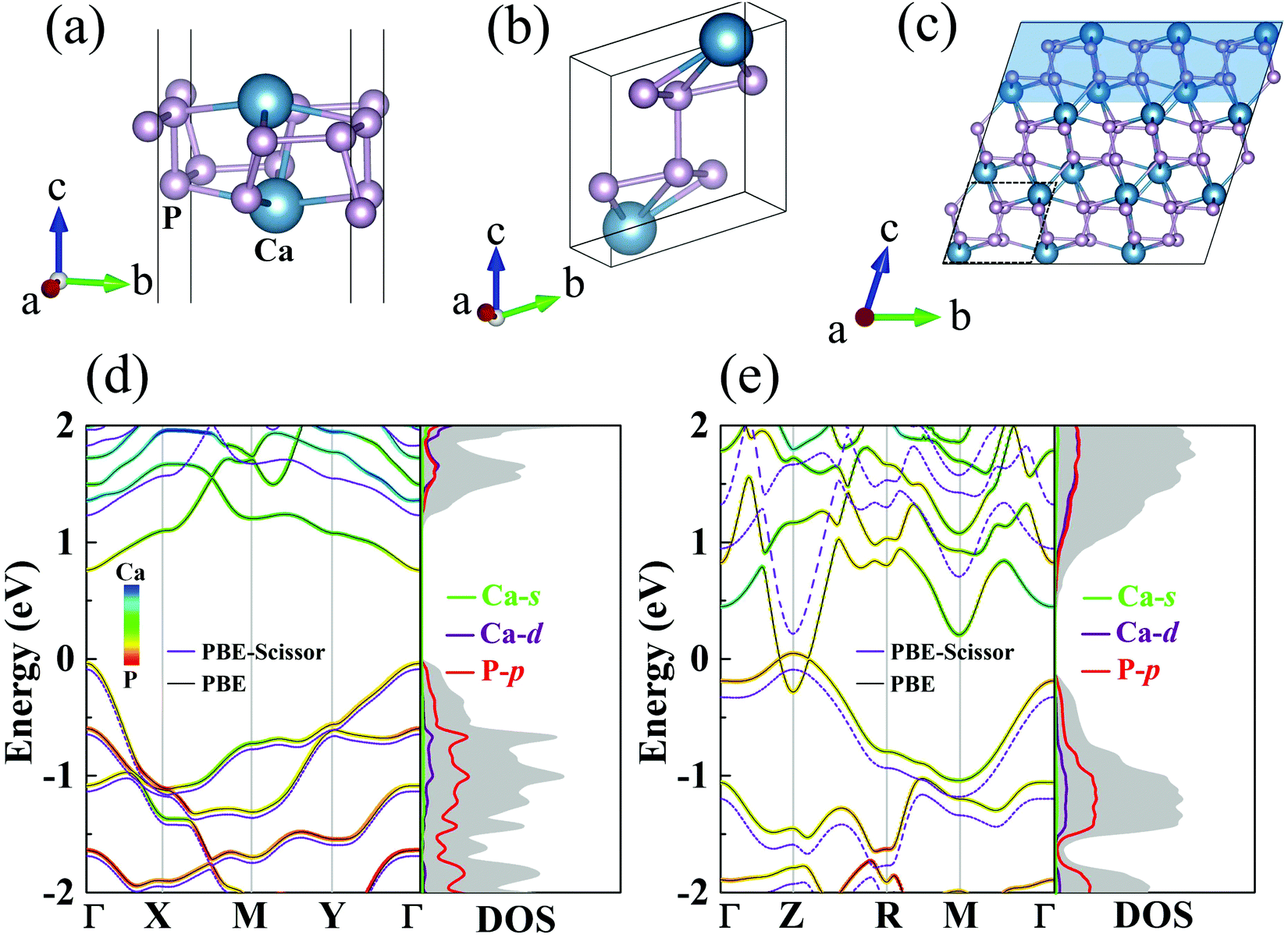
The crystal structures of the monolayer and bulk forms of CaP3 are shown in Fig. 1(a) and (b), respectively. Monolayer CaP3 has P![[1 with combining macron]](https://www.rsc.org/images/entities/char_0031_0304.gif) (no. 2) symmetry with 8 atoms in its unit cell. Unlike 2D InP3 and GeP3,30,34 the CaP3 monolayer possesses a specific cage configuration. As shown in Fig. 1(c), we can see clearly that it exhibits a rough surface and boundary, which would greatly enhance the phonon scattering.46 For the bulk, it also has P(no. 2) symmetry like the monolayer, and can be viewed as a phosphorus dimer with the insertion of calcium atoms at vacancy sites. Interestingly, the optimized lattice constants of bulk CaP3 are a = 5.60 Å, b = 5.68 Å, and c = 5.62 Å, very close to its experimental values,15 as shown in Table 1. According to the formula in ref. 47, the formation enthalpy of bulk CaP3 is calculated to be about −1.62 eV, which guarantees its stability against decomposition to the parent elements. Meanwhile, the theoretical optimized lattice constants of the CaP3 monolayer are a = 5.59 Å and b = 5.71 Å, which have slight differences with respect to the corresponding values of its bulk. This is mainly because the crystal structure of the monolayer gets a little loose without interlayer interaction. More details about the structural parameters are displayed in Table 1.
(no. 2) symmetry with 8 atoms in its unit cell. Unlike 2D InP3 and GeP3,30,34 the CaP3 monolayer possesses a specific cage configuration. As shown in Fig. 1(c), we can see clearly that it exhibits a rough surface and boundary, which would greatly enhance the phonon scattering.46 For the bulk, it also has P(no. 2) symmetry like the monolayer, and can be viewed as a phosphorus dimer with the insertion of calcium atoms at vacancy sites. Interestingly, the optimized lattice constants of bulk CaP3 are a = 5.60 Å, b = 5.68 Å, and c = 5.62 Å, very close to its experimental values,15 as shown in Table 1. According to the formula in ref. 47, the formation enthalpy of bulk CaP3 is calculated to be about −1.62 eV, which guarantees its stability against decomposition to the parent elements. Meanwhile, the theoretical optimized lattice constants of the CaP3 monolayer are a = 5.59 Å and b = 5.71 Å, which have slight differences with respect to the corresponding values of its bulk. This is mainly because the crystal structure of the monolayer gets a little loose without interlayer interaction. More details about the structural parameters are displayed in Table 1.
 |
| | Fig. 1 Crystal structures for the (a) monolayer and (b) bulk forms of CaP3. (c) Side view of the bulk supercell. The shallow region is the exfoliated monolayer structure. The orbital-resolved band structures and DOSs for the (d) monolayer and (e) bulk from PBE (solid lines) and PBE-Scissor (dashed lines). Note that we only present the DOSs after scissor shifting. | |
Table 1 Structural symmetry as well as our calculated lattice parameters (a, b, and c in Å) and band gaps (in eV) based on the PBE and HSE06 methods for the monolayer and bulk forms of CaP3. Available experimental and previous theoretical values are also listed for comparison
| Type |
Symmetry |
a
|
b
|
c
|
PBE |
HSE06 |
Ref. |
| Monolayer |
P(no. 2) |
5.59 |
5.71 |
— |
0.76 |
1.26 |
This work |
| Bulk |
P(no. 2) |
5.60 |
5.68 |
5.62 |
0 |
0.33 |
This work |
| Monolayer |
P(no. 2) |
5.59 |
5.71 |
— |
0.69 |
1.15 |
Thero.14 |
| Bulk |
P(no. 2) |
5.59 |
5.67 |
5.62 |
— |
— |
Expt15 |
As shown in Fig. 1, we present our computed orbital-resolved band structures and corresponding density of states (DOS), which are closely related to the Seebeck coefficients, for the monolayer and bulk. At the PBE level, the semimetal feature of the bulk35 is well reproduced, while the band gap for monolayer CaP3 is predicted to be around 0.76 eV (see Table 1). This value is close to the result reported in one recent study with PBE.14 On the basis of the HSE06 functional, as shown in Fig. S1 in the ESI,†![[thin space (1/6-em)]](https://www.rsc.org/images/entities/char_2009.gif) 48 we find that the band gap of the monolayer is 1.26 eV and that of its bulk is 0.33 eV, which are very close to the values reported in one recent theoretical study.14 Similar to previous studies,14,35 at the HSE06 level, the monolayer (bulk) form is a direct band gap semiconductor with the valence band maximum (VBM) and the conduction band minimum (CBM) both located at the Γ (Z) point. The same as the band gaps of Bi2O2Se (1.01 to 2.12 eV from the bulk to the monolayer),49 the band gaps of CaP3 also increase with the dimensionality reduction, indicating the strong dependence on the layer thickness due to the quantum confinement effect. Near the Fermi level, it can be seen clearly that the conduction band (CB) is evenly derived from hybridization of P-p and Ca-d, whereas the valence band (VB) is mainly occupied by P-p orbitals for those two forms. Consistent with previous reports,14 Ca-s has almost no contribution to the band structure. From the computed DOS, we can see a stair-shape DOS and steep slopes near the Fermi energy level for the monolayer, which are beneficial to its Seebeck coefficients. In addition, we find that the band edge states do not show spin–orbit splitting behavior after including spin–orbit coupling. This mainly due to the small difference between the masses of Ca and P atoms. Besides, comparing the band structures from PBE and HSE06, we find that the band dispersions are relatively unchanged. The HSE06 band structure can be almost reproduced by conducting a rigid shift of the PBE one. Thus, we conduct a scissor shift of the band structures and DOSs from PBE for both the bulk and monolayer forms to amend them to close to those obtained with HSE (see Fig. 1). As known, the computational demand with HSE06 is very expensive and goes beyond our ability. For simplicity, we call this method PBE-Scissor. In the following, in calculating the electronic transport properties as well as ZT, we use the data of the electronic structures from PBE-Scissor, not PBE.
48 we find that the band gap of the monolayer is 1.26 eV and that of its bulk is 0.33 eV, which are very close to the values reported in one recent theoretical study.14 Similar to previous studies,14,35 at the HSE06 level, the monolayer (bulk) form is a direct band gap semiconductor with the valence band maximum (VBM) and the conduction band minimum (CBM) both located at the Γ (Z) point. The same as the band gaps of Bi2O2Se (1.01 to 2.12 eV from the bulk to the monolayer),49 the band gaps of CaP3 also increase with the dimensionality reduction, indicating the strong dependence on the layer thickness due to the quantum confinement effect. Near the Fermi level, it can be seen clearly that the conduction band (CB) is evenly derived from hybridization of P-p and Ca-d, whereas the valence band (VB) is mainly occupied by P-p orbitals for those two forms. Consistent with previous reports,14 Ca-s has almost no contribution to the band structure. From the computed DOS, we can see a stair-shape DOS and steep slopes near the Fermi energy level for the monolayer, which are beneficial to its Seebeck coefficients. In addition, we find that the band edge states do not show spin–orbit splitting behavior after including spin–orbit coupling. This mainly due to the small difference between the masses of Ca and P atoms. Besides, comparing the band structures from PBE and HSE06, we find that the band dispersions are relatively unchanged. The HSE06 band structure can be almost reproduced by conducting a rigid shift of the PBE one. Thus, we conduct a scissor shift of the band structures and DOSs from PBE for both the bulk and monolayer forms to amend them to close to those obtained with HSE (see Fig. 1). As known, the computational demand with HSE06 is very expensive and goes beyond our ability. For simplicity, we call this method PBE-Scissor. In the following, in calculating the electronic transport properties as well as ZT, we use the data of the electronic structures from PBE-Scissor, not PBE.
3.2 Electrical transport properties
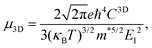
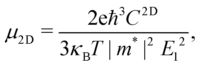
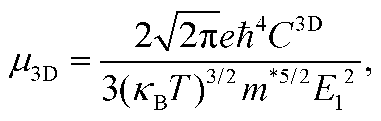
Using deformation potential (DP) theory,50 we can calculate the carrier mobility μ of the monolayer and bulk phases. Meanwhile, the corresponding electron relaxation time τe can be also obtained, which is a vital physical quantity for accurately evaluating the ZT value. For the two systems, μ and τe can be calculated by the formula as follows:| |  | (2) |
| |  | (3) |
| |  | (4) |
where C2D = [∂2E/∂δ2]/S (C3D = [∂2E/∂δ2]/V) is the elastic modulus for the 2D (3D) system, m* = ħ2/[∂2ε/∂k2] is the effective mass, kB is the Boltzmann constant, and E1 = dEedge/dδ is the DP constant.51,52 All our calculated parameters are summarized in Table 2. On the whole, we can find that the two forms both have relatively high electron carrier mobilities, which are much higher than that of monolayer MoS2 (60–200 cm2 V−1 s−1).53 Surprisingly, the carrier mobility of holes exhibits a very small value of 46.32 cm2 V−1 s−1 with a tiny relaxation time of 0.03 ps for the monolayer along the a direction. The effective mass for holes along a is a factor of 3 larger than that for holes along b for the monolayer structure. Such obvious anisotropic behavior for holes originates from its VB structure, which is mainly contributed by the P-py orbital. For the VB near the Fermi level, the contributions from the P-px,z and Ca-dxy,x2−y2 orbitals are limited, while those from other d-orbitals are neglectable. As illustrated in Fig. 1, the first VB bends differently along Γ–X and Γ–Y, which corresponds to the crystallographic directions of a and b, respectively. As a result, the electron velocity vi,k = [∂ε/∂k]/ħ and the value of ∂2ε/∂k2 for holes along a are significantly smaller than the corresponding values for holes along b. Such anisotropy of the band structure is also responsible for the anisotropy of τe and also σ as presented in Table 2 and Fig. 2(a). The electron masses along a and b for the monolayer structure are almost the same. Such isotropy is from the isotropy of the first CB along Γ–X and Γ–Y in the BZ. As shown in Fig. 1, the CB is mainly derived from the hybridization of P-p and Ca-d orbitals. Here, all three P-p and five Ca-d orbitals have contributions.
Table 2 Calculated DP constant E1, elastic modulus C, effective mass m*, electron and hole carrier mobilities μ, and relaxation time τe at 300 K for the monolayer and bulk. a and b are crystallographic directions
| Compound |
Carrier type |
E
1 (eV) |
C (J m−2; GPa) |
m* (m0) |
μ (cm2 V−1 s−1) |
τ
e (ps) |
| Monolayer |
Electron (a) |
0.57 |
52.71 |
0.89 |
2932.98 |
1.48 |
| Hole (a) |
3.45 |
52.71 |
1.17 |
46.32 |
0.03 |
| Electron (b) |
1.13 |
63.92 |
0.95 |
794.19 |
0.43 |
| Hole (b) |
3.02 |
63.92 |
0.39 |
659.71 |
0.14 |
|
|
| Bulk |
Electron (a) |
4.06 |
126.07 |
0.45 |
3488.19 |
0.89 |
| Hole (a) |
7.24 |
126.07 |
0.42 |
1304.39 |
0.31 |
| Electron (b) |
6.33 |
132.02 |
0.41 |
1896.75 |
0.44 |
| Hole (b) |
8.82 |
132.02 |
0.43 |
864.11 |
0.21 |
 |
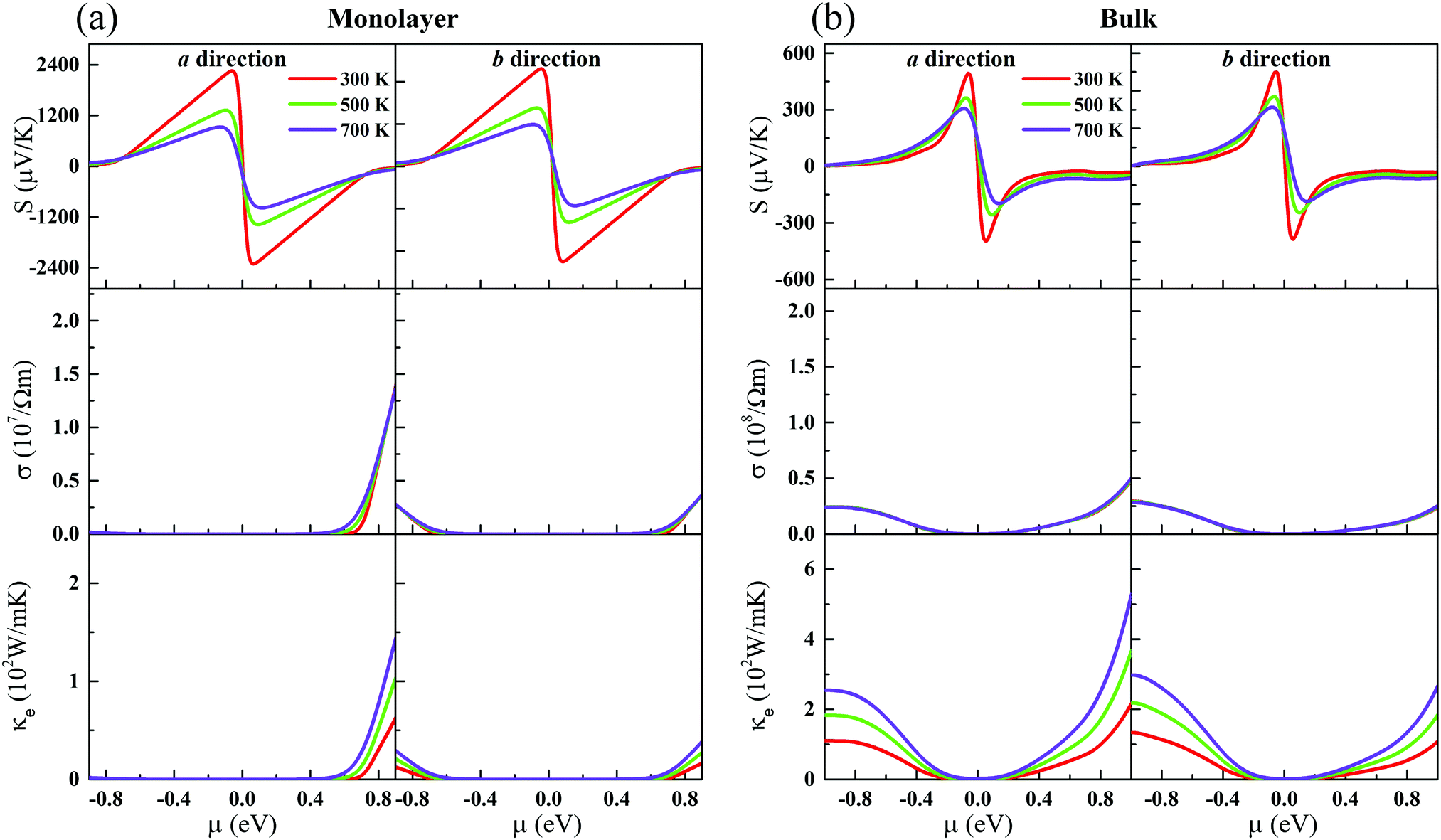
| | Fig. 2 The Seebeck coefficients (the first-layer panels), electrical conductivity (the second-layer panels), and electronic thermal conductivity (the last-layer panels) at different temperatures along the a and b directions, as functions of the chemical potential for the (a) monolayer and (b) bulk. | |
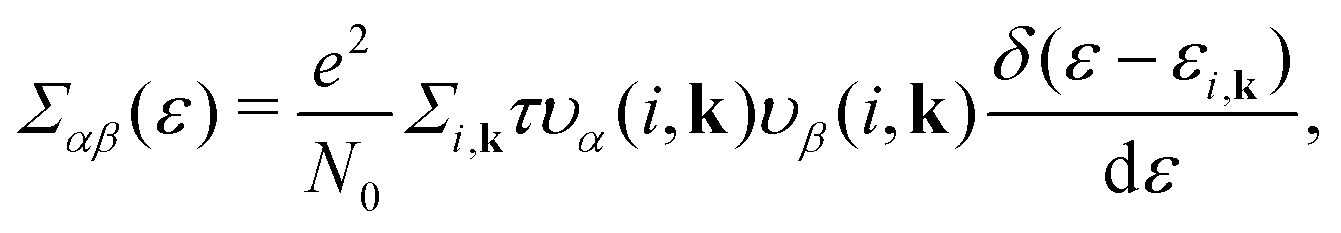
Based on the semiclassical Boltzmann transport theory and the constant scattering time approximation, we calculate the electrical transport coefficients, including the Seebeck coefficient, electrical conductivity and electrical thermal conductivity. To confirm the doping effects on the electronic transport, the rigid band approximation is employed. In this approximation, the electronic structure is deemed to be unchanged with doping and only the Fermi level is modulated. Herein, these transport coefficients can be defined by the following formula,41
| |  | (5) |
| |  | (6) |
| |  | (7) |
where
αβ and
Σαβ(
ε) are Cartesian indices and the transport distribution function, respectively. A series of calculated electrical transport properties are presented in
Fig. 2. The Seebeck coefficient is nearly isotropic for the monolayer and bulk. Meanwhile, we can see clearly that the Seebeck coefficient of the monolayer shows a dramatic increase compared to its bulk form. At room temperature, the maximum Seebeck coefficients along the
a and
b directions can reach 2250 (557) and 2290 (568) μV K
−1 for the monolayer (bulk), respectively. The Seebeck coefficients of the monolayer are fundamentally larger than those of the bulk. Such a large difference mainly originates from their different electronic structures. As has been reported, the Seebeck coefficient vanishes when the Fermi level is at the Weyl nodes.
54 Compared with the Weyl semimetal TaAs (∼80 μV K
−1),
55 bulk CaP
3 exhibits very large values of the Seebeck coefficients.
To further study the transport properties, we calculate the electrical conductivity σ with respect to the chemical potential, as shown in Fig. 2. Obviously, unlike the Seebeck coefficients, σ is less sensitive with respective to the temperature. σ of CaP3 exhibits an obvious anisotropic behavior. σ along the b direction is visibly larger than that along the a direction, originating from the anisotropy of the crystal structure. Meanwhile, we can also find that σ of p-type doping is higher than that of the n-type for the two forms along the b direction in the low chemical potential region (−0.5 eV to 0.5 eV). It is found that σ gets larger and larger with increasing μ, while the Seebeck coefficient achieves a peak value near the Fermi level. This could better balance S and σ and can give rise to a high power factor. We note that the slope of σ for the bulk is relatively flat when compared with that of the monolayer, which can be attributed to their different DOSs as shown in Fig. 1. In addition, σ of the bulk is larger than that of its monolayer.
Note that the electrical transport properties of our studied systems are hardly affected under considering the role of spin-degeneracy. After comparing the Seebeck coefficients as well as σ based on non-spin polarized calculations and spin-degeneracy calculations along the a direction for both the bulk and monolayer forms of CaP3, the differences are invisible.
In general, the total thermal conductivity is mainly contributed by κl and κe in non-degenerate semiconductors. We calculate κe of CaP3 based on the Wiedemann–Franz law,56
where
L is the Lorenz number. Usually,
L is equal to (π
kB)
2/3
e2 for calculation of TE materials. Similar to
σ,
κe is strongly anisotropic as well (see
Fig. 2). Actually, it is almost proportional to
σ at a specific temperature. Increasing chemical potential would increase its sensitivity with respect to the temperature. The same as
σ,
κe of the bulk is also larger than that of its monolayer.
3.3 Phonon spectrum and atomic vibration mode
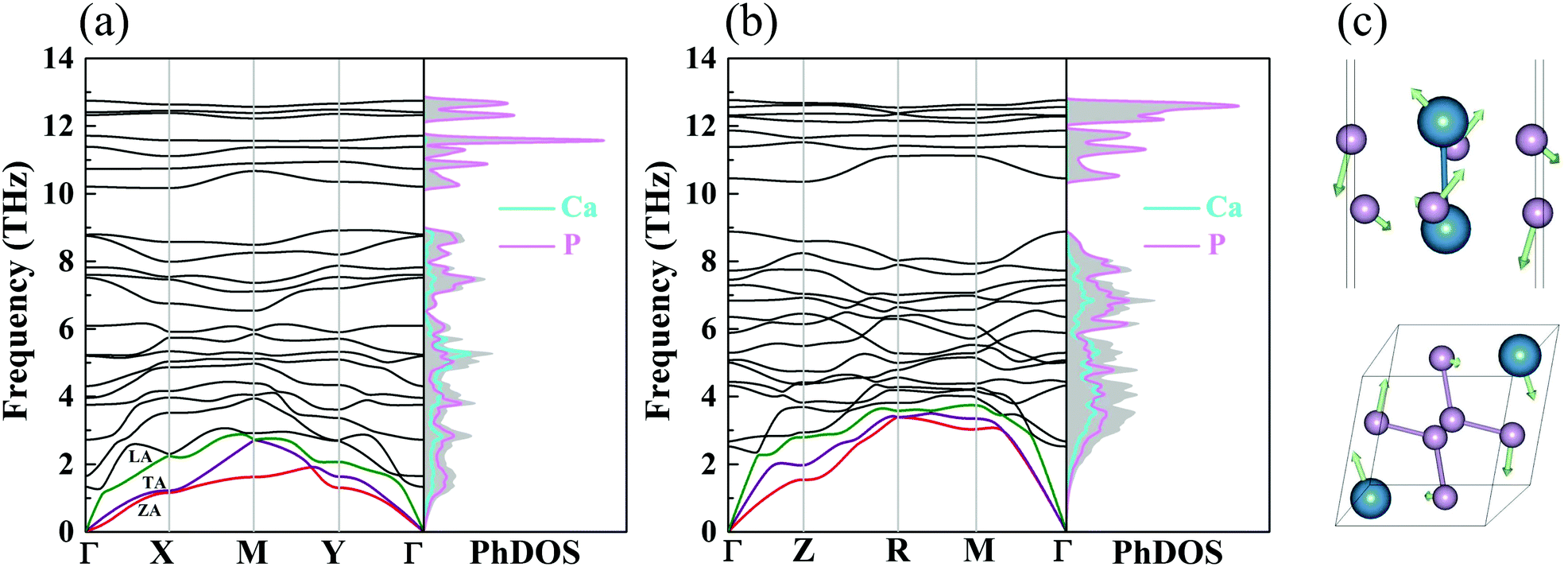
Based upon the 2nd IFCs and using the Phonopy code45 as well as VASP, we obtain the phonon dispersions and partial atomic phonon density of states (PhDOS) of CaP3, as shown in Fig. 3(a) and (b). The phonon branches can be arranged on the basis of the continuity of their eigenvectors57| |  | (9) |
where  is the displacement of atom j in the eigenvector of the vibrational mode and Δ is a small wave vector. Since the acoustic branches play a major contributing role for thermal transport, the acoustic branches are highlighted with different colors while the optical branches are presented in black. As shown, there are no negative frequencies in the BZ, guaranteeing dynamic stability for both forms of CaP3. Herein, we can see clearly that the monolayer exhibits linear components in the ZA dispersion curve. It is reported that the lattice thermal conductivity of the linear components in the ZA mode may be larger than that of the quadratic, due to the larger density of states of the quadratic branch.58 The lowest frequency of the optical modes at the Γ point is 1.3 and 2.5 THz for the monolayer and bulk, respectively. In general, these low optical modes are beneficial to low thermal conductivity.59 Besides, it can be clearly seen that the frequency gaps near 9–10 THz separate the optical branches into low-frequency and high-frequency areas. The amplitudes of these frequency gaps are 1.4 and 1.6 THz for the monolayer and bulk, respectively. Additionally, the monolayer exhibits lower and flatter acoustic branches compared to the bulk form, especially for the ZA mode, leading to smaller phonon velocities and lower lattice thermal conductivities.
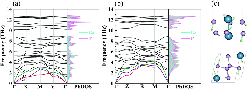 |
| | Fig. 3 The phonon dispersions and partial PhDOS of the (a) monolayer and (b) bulk. The red, purple and green lines are ZA, TA and LA modes. (c) The corresponding vibrational modes of the lowest optical branch at the Γ point for the monolayer and bulk. | |
From the corresponding PhDOS, one can see clearly that the Ca and P atomic vibrations equally dominate the low-frequency region, while the high-frequency region is fully occupied by the vibrations of P atoms for CaP3. Contrasting with its bulk form, the monolayer exhibits more cuspate peaks in the PhDOS, resulting in low phonon velocities. In addition, the corresponding vibrational modes of the lowest optical branch for the two forms at the Γ point are shown in Fig. 3(c). Simultaneously, disordered characteristic atomic vibrations can be seen. For the bulk, the Ca and P atoms move in opposite directions to one another, while the monolayer exhibits fierce movement along different directions. These disordered vibrations will greatly reduce the heat conductivity, leading to low thermal conductivity.60
3.4 Lattice thermal conductivity
In most cases, κl is greatly larger than κe, thus playing a critical role in measuring the heat transport ability of TE materials. Based on the iterative approach, κl can be computed according to61| | | κl,i = ΣλΣqcphυg,i2(q,λ)τ(q,λ). | (10) |
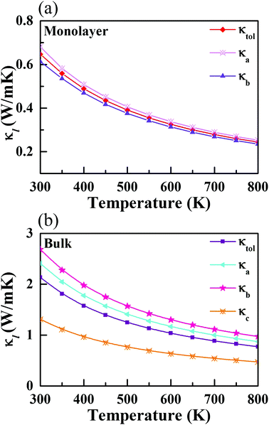
cph is the heat capacity per mode, υg,i(q,λ) is the phonon group velocity vector, and τ(q,λ) is the relaxation time of the phonon mode with wave vector q and dispersion branch λ. Herein, the total κl can be defined by κl = (κa + κb + κc)/3 and κl = (κa + κb)/2 for the bulk and monolayer forms, respectively. Note that the definition of κl is somewhat arbitrary for a low-dimensional system. Indeed, κl may be underestimated without considering the influence of the vacuum thickness in 2D materials. For monolayer CaP3, the effective thickness can be determined by a double-layer system which has the minimum energy stacking structure. Herein, an effective thickness of 7.74 Å is chosen to revise the undervalued κl. The κl values of the two materials along different directions, at temperatures from 300 to 800 K, are presented in Fig. 4. Obviously, we can see that κl possesses evident temperature dependent behavior and is proportional to 1/T, which is mainly attributed to the enhancement of intrinsic scattering with the temperature increasing. It is noteworthy that κl of the monolayer is 0.65 W m−1 K−1 at room temperature, which is much lower than those of many 2D layered materials, such as phosphorene (∼83.5 W m−1 K−1)62 and layered MoS2 (∼23.2 W m−1 K−1).60 Compared with κl of Weyl semimetal TaAs (39.26 W m−1 K−1 at 300 K),63 the bulk form (2.14 W m−1 K−1) also shows absolute superiority in thermal transport. When the system changes from the bulk to the monolayer, we can find that κl has a significant reduction. Unlike κl of the monolayer (κa > κb), the bulk shows an inverse trend with the following order: κb > κa, which mainly originates from the characteristic atomic configuration. Interestingly, contrary to graphene,64 the value of κl gradually increases with the increase of the number of layers for the CaP3 crystal structure. To further analyze their intrinsic low κl and these differences, we calculate the correlative phonon transport properties, which will be systematically studied in the next section.
 |
| | Fig. 4 Calculated lattice thermal conductivity along different directions for the (a) monolayer and (b) bulk. | |
3.5 Phonon transport properties
The phonon velocity is a direct physical quantity for evaluating thermal transportation. Based on our calculated phonon spectrum, the phonon group velocities can be calculated by| |  | (11) |
where ωi(q) is the phonon frequency. The phonon group velocities are presented in Fig. 5(a), and the acoustic phonon group velocities for the ZA, TA, and LA modes are highlighted with different colors. As we predicted above, the average of the acoustic group velocities of the monolayer (3.23 km s−1) is fairly lower than that of the bulk (4.52 km s−1), particularly for the ZA and TA modes, which will give rise to a decreasing behavior of κl. This is mainly attributed to the more flat and relatively low acoustic modes for the monolayer, as shown in Fig. 3. Specifically, the phonon velocities of the two transverse (ZA and TA) modes and one longitudinal (LA) mode are 1.39, 2.12, and 6.19 km s−1 for the monolayer at the Γ point, respectively, which are lower than the corresponding values of 3.21, 4.13, and 6.23 km s−1 for the bulk. More details of the phonon transport are summarized in Table 3.
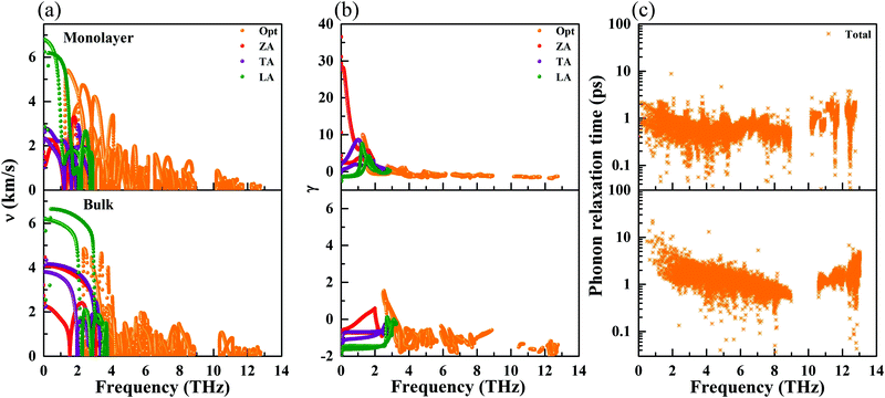 |
| | Fig. 5 Calculated phonon group velocity (a), Grüneisen parameters (b), and phonon relaxation time (c) for the monolayer and bulk at 300 K. | |
Table 3 Summary of the lowest optical frequency ωo,min at the Γ point (in THz), lattice thermal conductivity (κl in W m−1 K−1), transverse (ZA/TA) and longitudinal (LA) phonon group velocities (υZA/TA/LA in km s−1) and average Grüneisen parameters (![[small gamma, Greek, macron]](https://www.rsc.org/images/entities/i_char_e0c4.gif) ZA/TA/LA) for the monolayer and bulk
ZA/TA/LA) for the monolayer and bulk
| Type |
ω
o,min
|
κ
l
|
υ
ZA
|
υ
TA
|
υ
LA
|
ZA
|
TA
|
LA
|
| Monolayer |
1.32 |
0.65 |
1.39 |
2.12 |
6.19 |
6.57 |
3.12 |
1.21 |
| Bulk |
2.52 |
2.14 |
3.21 |
4.13 |
6.23 |
0.59 |
0.75 |
0.72 |
To further study the phonon transport properties, we calculated the corresponding Grüneisen parameters and phonon relaxation time. The Grüneisen parameter can qualitatively characterize the anharmonic interactions of materials. It can be defined by
| | 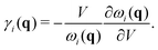 | (12) |
In general, large
γ means the existence of strong phonon–phonon anharmonic scattering,
65 leading to low
κl. To effectively evaluate the anharmonicity, the Grüneisen parameters of acoustic modes are plotted in
Fig. 5(b). Surprisingly, the monolayer exhibits ultrahigh values of the Grüneisen parameters of ∼30, which are much larger than those of the bulk form. Additionally, the lone-pair electrons and the nonbonding electrons can interact with the valence electrons of neighboring atoms, leading to large Grüneisen parameters at limited temperature. As shown in
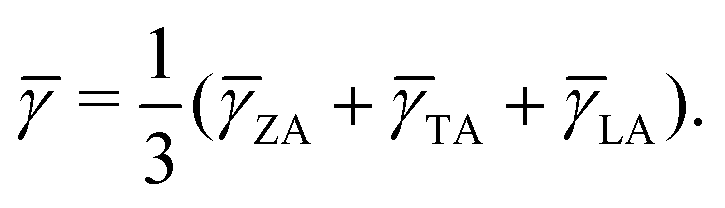
Fig. 5(b), we can see clearly that the large Grüneisen parameters mainly exist in the low-frequency area, which is a typical behavior for heat transport in materials. The average of the acoustic Grüneisen parameters can be obtained by,
66,67| |  | (13) |
| |  | (14) |
The calculated
can reach 3.63 for monolayer CaP
3. This value is comparable to the average Grüneisen parameters of low
κl compounds, such as SnSe (2.83)
66 and PbTe (1.45).
68 From
Table 3, we can also find that the monolayer shows large
compared to the bulk, indicating that it possesses stronger anharmonicity than the bulk. This explains to some extent why
κl of the monolayer is lower than that of the bulk. Generally, strongly anharmonic materials require being measured using higher-order anharmonicity (four-phonon). On the basis of the three-phonon scattering, the four-phonon scattering can better evaluate the heat transport properties of materials.
69 However, the computation of the four-phonon scattering probabilities and the iterative solution is very difficult, which requires extremely large computation time and storage memory. Therefore, we don't consider the influence of four-phonon scattering in this work.
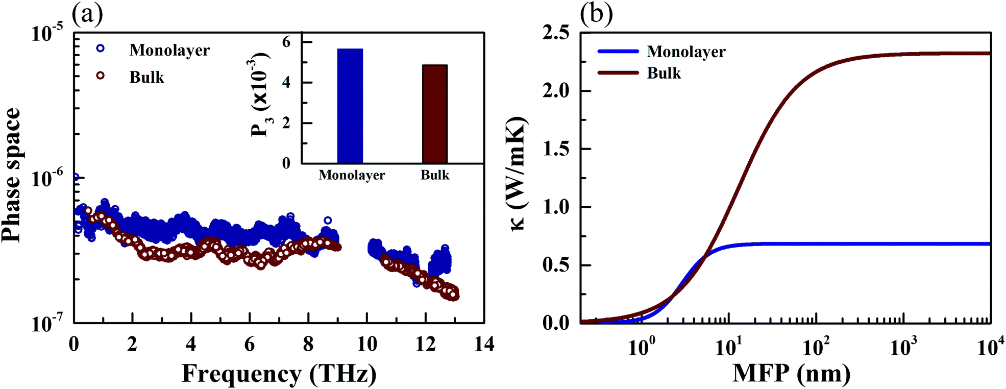
The phonon relaxation time is a significant factor to κl, and can be calculated from the anharmonic 3rd IFCs. The results of the phonon relaxation time are plotted in Fig. 5(c). We can see that the phonon relaxation time of the monolayer is dominantly shorter than that of the bulk, indicating that the monolayer has stronger phonon scattering. As shown in Fig. 6(a), we calculate the three phonon scattering phase space (P3). It can be used to qualitatively analyze the magnitude of the phonon scattering. P3 can be written as70
| |  | (15) |
| |  | (16) |
where
Ω and
Dj(±) are a normalization factor, and the absorption and emission processes, respectively. Obviously, we find that the monolayer has a larger scattering phase space than that of the bulk phase, which implies that the monolayer possesses more phase space allowing phonon–phonon scattering, resulting in a shorter phonon relaxation time and lower
κl.
 |
| | Fig. 6 Calculated three phonon scattering phase space (a) and cumulative lattice thermal conductivity along the a direction (b) for the monolayer and bulk CaP3 at 300 K. (Inset) Total three phonon scattering phase space. | |
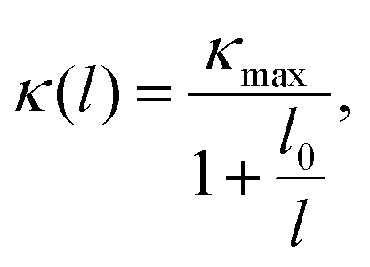
Investigating the size effect of a TE material can help people to further regulate the thermal conductivity in designing TE nanostructures.71,72 It can be evaluated in terms of the phonon MFP. When the size of a TE device is shorter than that of the phonon MFP, κl would be significantly depressed by the frequent phonon-surface scattering. In the present work, the MFP is obtained by fitting the cumulative κl,
| |  | (17) |
where
κmax is the ultimate thermal conductivity and
l0 is the evaluated characteristic phonon MFP. A comparison of the cumulative
κl of the monolayer and bulk at 300 K can be found in
Fig. 6(b). One can see that the cumulative
κl keeps increasing as
l increases, until reaching the thermodynamic limit. Additionally, the values of
l0 are 4.07 and 12.62 nm for the monolayer and bulk at 300 K, respectively. In general, nanostructures with
l0 longer than 100 nm possess a relatively sensitive size effect. Compared with TaAs, which possesses an
l0 of 110 nm,
63 the size dependence of
κl for CaP
3 is not sensitive.
3.6 Thermoelectric figure of merit
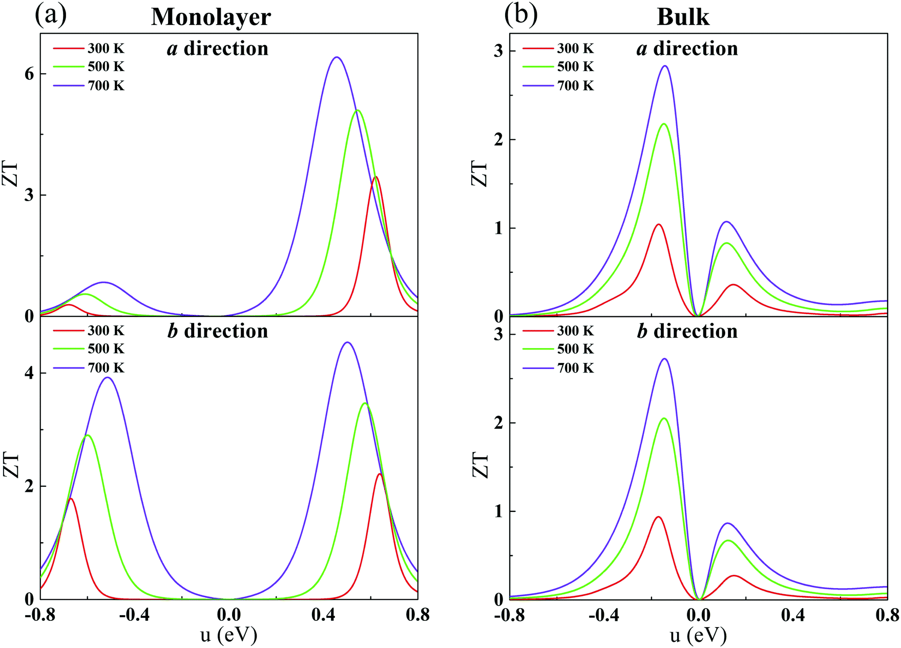
Combining our calculated phononic and electronic transport coefficients, we estimate ZT for monolayer and bulk CaP3. The constant τe (Table 2) is adopted. As shown in Fig. 7, the calculated ZT as a function of chemical potential for CaP3 is presented at typical temperatures of 300, 500 and 700 K. Surprisingly, we find that the maximum value of ZT at 700 K can reach 6.39 along the a direction for the monolayer, which is markedly higher than that of the bulk phase, ∼2.83. Such a high ZT value is comparable to several star TE materials, such as the ZrSe2/HfSe2 superlattice-monolayer structure (ZT = 5.3 at 300 K),73 thin-film Fe2V0.8W0.2Al (ZT = 5 around 300–400 K),74 monolayer SnP3 (6.10 at 500 K)75 and InP3 (5.16 at 700 K).33
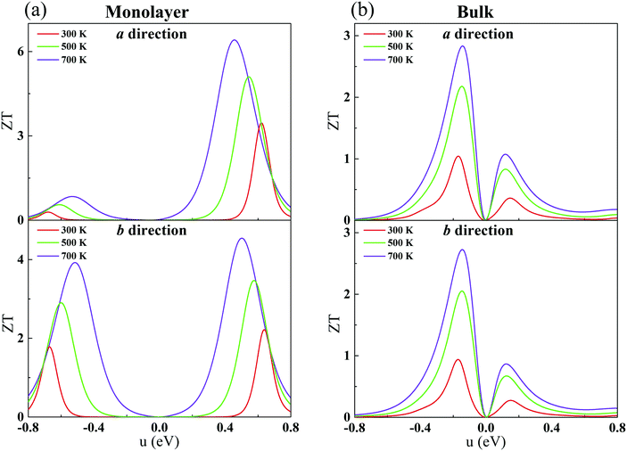 |
| | Fig. 7 Calculated ZT with respect to the chemical potential for the monolayer (a) and bulk (b) along the a and b directions. | |
Additionally, for the monolayer, one can see that ZT of the n-type is much higher than that of the p-type along the a direction. After carefully comparing the electronic and lattice transport parameters for the n- and p-types, we find that the large anisotropy of ZT is from the big differences in the electrical conductivity σ. The values of the relaxation time τe listed in Table 2 are very different for the n- and p-types, by almost two orders of magnitude. As clearly indicated in Table 2, since the effective masses (as well as the elastic modulus) for the n- and p-types along the a direction in the monolayer have the same order of magnitude, according to eqn (2) and (4), we know that the anisotropy of ZT is mainly from the different values of the carrier mobilities μ and different DP constant E1. According to the formulas of the DP constant and the electron–phonon coupling (EPC) matrix element under the thermodynamic average  ,52 we find that the anisotropy of ZT is finally originating from the different EPC under the n- and p-types of doping. Although the EPC here is modeled by the DP theory in a very simple way, only considering the LA phonon scattering, our results still can be regarded as a good starting point for quantitatively analyzing the thermoelectric properties of CaP3.
Generally, when the ZT value of a material exceeds 1.0, it can be considered as an ideal TE material.76 Herein, it is noted that monolayer CaP3 exhibits excellent TE properties, which make it a candidate for TE applications. From the above results, we can conclude that the low-dimensional nanostructure technique can greatly improve the TE performances of CaP3 as well as similar layered materials.
In addition, we compare the electronic transport results as well as the ZT values obtained from PBE-Scissor with those from PBE in the ESI.†48 From Fig. S2–S5 (ESI†), we find that the PBE-Scissor method can greatly improve the results. Zero conductivity for an energy window equal to the HSE band gap centered around μ = 0 eV is successfully obtained by using PBE-Scissor.
4 Conclusion
In summary, we investigate the electronic structures, phonon vibrations, and TE properties of CaP3 in 3D bulk and 2D monolayer forms by using first-principles calculations and the Boltzmann transport equation. Our results show that the values of the Seebeck coefficients show great distinction between these two forms. Meanwhile, the electronic conductivity and the electronic thermal conductivity exhibit strong anisotropic behaviors. The intrinsic κl of the monolayer is extremely low, ∼0.65 W m−1 K−1 at 300 K, which can be attributed to its phonon transport properties, such as lower values of phonon velocities ∼1.41 km s−1, larger Grüneisen parameters ∼30, and shorter phonon relaxation time, when compared with the bulk. As a consequence, the monolayer exhibits excellent TE performance and the maximum ZT value can reach as high as 6.39 at 700 K, indicating that the CaP3 nano-thin film can be a promising candidate for TE applications. Therefore, our work provides a forceful theoretical basis for effective improvement of the TE conversion efficiency by low-dimensional nano-engineered technology.
Conflicts of interest
There are no conflicts to declare.
Acknowledgements
The calculations were performed at the Supercomputer Centre in the China Spallation Neutron Source. This work was financially supported by National Natural Science Foundation of China (NSFC) (Grant No. 11874145 and 12074381) and Guangdong Provincial Department of Science and Technology, China (No. 2018A0303100013).
References
- S. Chu, Y. Cui and N. Liu, Nat. Mater., 2016, 16, 16 CrossRef.
- M. Aneke and M. Wang, Appl. Energy, 2016, 179, 350–377 CrossRef.
- D. Champier, Energy Convers. Manage., 2017, 140, 167–181 CrossRef.
- J. Yang, L. Xi, W. Qiu, L. Wu, X. Shi, L. Chen, J. Yang, W. Zhang, C. Uher and D. J. Singh, npj Comput. Mater., 2016, 2, 15015 CrossRef CAS.
- W.-X. Zhou, Y. Cheng, K.-Q. Chen, G. Xie, T. Wang and G. Zhang, Adv. Funct. Mater., 2019, 1903829 Search PubMed.
- J. M. Skelton, S. C. Parker, A. Togo, I. Tanaka and A. Walsh, Phys. Rev. B: Condens. Matter Mater. Phys., 2014, 89, 205203 CrossRef.
- Y.-J. Zeng, D. Wu, X.-H. Cao, W.-X. Zhou, L.-M. Tang and K.-Q. Chen, Adv. Funct. Mater., 2019, 1903873 Search PubMed.
- Z. Wang, L. Zhao, K. F. Mak and J. Shan, Nano Lett., 2017, 17, 740–760 CrossRef CAS.
- Y. Pei, H. Wang and G. J. Snyder, Adv. Mater., 2012, 24, 6125–6135 CrossRef CAS.
- L. D. Hicks and M. S. Dresselhaus, Phys. Rev. B: Condens. Matter Mater. Phys., 1993, 47, 12727 CrossRef CAS.
- X. Y. Mi, X. Yu, K. L. Yao, X. Huang, N. Yang and J. T. Lü, Nano Lett., 2015, 15, 5229–5234 CrossRef CAS.
- G. Xie, D. Ding and G. Zhang, Adv. Phys. X, 2018, 3, 1480417 Search PubMed.
- M. Hu and D. Poulikakos, Nano Lett., 2012, 12, 5487–5494 CrossRef CAS.
- N. Lu, Z. Zhuo, H. Guo, P. Wu, W. Fa, X. Wu and X. C. Zeng, J. Phys. Chem. Lett., 2018, 9, 1728–1733 CrossRef CAS.
- W. Dahlmann and H. Schnering, Naturwissenschaften, 1973, 60, 518 CrossRef CAS.
- K. S. Novoselov, A. K. Geim, S. V. Morozov, D. Jiang, Y. Zhang, S. V. Dubonos, I. V. Grigorieva and A. A. Firsov, Science, 2004, 306, 666–669 CrossRef CAS.
- X.-K. Chen, J. Liu, Z.-X. Xie, Y. Zhang, Y.-X. Deng and K.-Q. Chen, Appl. Phys. Lett., 2018, 113, 121906 CrossRef.
- B.-Y. Cao, J.-H. Zou, G.-J. Hu and G.-X. Cao, Appl. Phys. Lett., 2018, 112, 041603 CrossRef.
- A. Kara, H. Enriquez, A. P. Seitsonen, L. L. Y. Voon, S. Vizzini, B. Aufray and H. Oughaddou, Surf. Sci. Rep., 2012, 67, 1–18 CrossRef CAS.
- W.-B. Zhang, Z.-B. Song and L.-M. Dou, J. Mater. Chem. C, 2015, 3, 3087–3094 RSC.
- H. Liu, A. T. Neal, Z. Zhu, Z. Luo, X. Xu, D. Tománek and P. D. Ye, ACS Nano, 2014, 8, 4033–4041 CrossRef CAS.
- W. Yu, Z. Zhu, S. Zhang, X. Cai, X. Wang, C.-Y. Niu and W.-B. Zhang, Appl. Phys. Lett., 2016, 109, 103104 CrossRef.
- D. Li, J. Gao, P. Cheng, J. He, Y. Yin, Y. Hu, L. Chen, Y. Cheng and J. Zhao, Adv. Funct. Mater., 2019, 1904349 Search PubMed.
- J. He, D. Li, Y. Ying, C. Feng, J. He, C. Zhong, H. Zhou, P. Zhou and G. Zhang, npj Comput. Mater., 2019, 5, 47 CrossRef.
- Z. Ding, M. An, S. Mo, X. Yu, Z. Jin, Y. Liao, K. Esfarjani, J. T. Lü, J. Shiomi and N. Yang, J. Mater. Chem. A, 2019, 7, 2114–2121 RSC.
- X.-L. Zhu, P.-F. Liu, J. Zhang, P. Zhang, W.-X. Zhou, G. Xie and B.-T. Wang, Nanoscale, 2019, 11, 19923–19932 RSC.
- X.-L. Zhu, H. Yang, W.-X. Zhou, B. Wang, N. Xu and G. Xie, ACS Appl. Mater. Interfaces, 2020, 12, 36102–36109 CrossRef CAS.
- F. Shojaei and H. S. Kang, J. Mater. Chem. C, 2017, 5, 11267–11274 RSC.
- H.-H. Wu, H. Huang, J. Zhong, S. Yu, Q. Zhang and X. C. Zeng, Nanoscale, 2019, 11, 12210–12219 RSC.
- Y. Jing, Y. Ma, Y. Li and T. Heine, Nano Lett., 2017, 17, 1833–1838 CrossRef CAS.
- S. Sun, F. Meng, H. Wang, H. Wang and Y. Ni, J. Mater. Chem. A, 2018, 6, 11890–11897 RSC.
- S. Yao, X. Zhang, Z. Zhang, A. Chen and Z. Zhou, Int. J. Hydrogen Energy, 2019, 44, 5948–5954 CrossRef CAS.
- T. Ouyang, E. Jiang, C. Tang, J. Li, C. He and J. Zhong, J. Mater. Chem. A, 2018, 6, 21532–21541 RSC.
- N. Miao, B. Xu, N. C. Bristowe, J. Zhou and Z. Sun, J. Am. Chem. Soc., 2017, 139, 11125–11131 CrossRef CAS.
- Q. Xu, R. Yu, Z. Fang, X. Dai and H. Weng, Phys. Rev. B, 2017, 95, 045136 CrossRef.
- G. Kresse and J. Furthmüller, Phys. Rev. B: Condens. Matter Mater. Phys., 1996, 54, 11169 CrossRef CAS.
- P. E. Blöchl, Phys. Rev. B: Condens. Matter Mater. Phys., 1994, 50, 17953 CrossRef.
- G. Kresse and D. Joubert, Phys. Rev. B: Condens. Matter Mater. Phys., 1999, 59, 1758–1775 CrossRef CAS.
- J. Klimeš, D. R. Bowler and A. Michaelides, J. Phys.: Condens. Matter, 2010, 22, 022201 CrossRef.
- J. Heyd, G. E. Scuseria and M. Ernzerhof, J. Chem. Phys., 2003, 118, 8207–8215 CrossRef CAS.
- G. K. H. Madsen and D. J. Singh, Comput. Phys. Commun., 2006, 175, 67–71 CrossRef CAS.
- L. Chaput, P. Pécheur and H. Scherrer, Phys. Rev. B: Condens. Matter Mater. Phys., 2007, 75, 045116 CrossRef.
- D. Parker and D. J. Singh, Phys. Rev. B: Condens. Matter Mater. Phys., 2010, 82, 035204 CrossRef.
- W. Li, J. Carrete, N. A. Katcho and N. Mingo, Comput. Phys. Commun., 2014, 185, 1747–1758 CrossRef CAS.
- A. Togo, F. Oba and I. Tanaka, Phys. Rev. B: Condens. Matter Mater. Phys., 2008, 78, 134106 CrossRef.
- H. Xiao, W. Cao, T. Ouyang, X. Xu, Y. Ding and J. Zhong, Appl. Phys. Lett., 2018, 112, 233107 CrossRef.
- C. Wolverton and V. Ozoliņš, Phys. Rev. B: Condens. Matter Mater. Phys., 2006, 73, 144104 CrossRef.
- See the ESI† for the electronic transport properties and ZT obtained with PBE and PBE-Scissor.
- X. L. Zhu, P. F. Liu, G. Xie and B. T. Wang, Phys. Chem. Chem. Phys., 2019, 21, 10931–10938 RSC.
- J. Bardeen and W. Shockley, Phys. Rev., 1950, 80, 72–80 CrossRef CAS.
- Y. Cai, G. Zhang and Y. W. Zhang, J. Am. Chem. Soc., 2014, 136, 6269–6275 CrossRef CAS.
- J. Xi, M. Long, L. Tang, D. Wang and Z. Shuai, Nanoscale, 2012, 4, 4348–4369 RSC.
- M. M. Perera, M.-W. Lin, H.-J. Chuang, B. P. Chamlagain, C. Wang, X. Tan, M. M.-C. Cheng, D. Tománek and Z. Zhou, ACS Nano, 2013, 7, 4449–4458 CrossRef CAS.
- R. Lundgren, P. Laurell and G. A. Fiete, Phys. Rev. B: Condens. Matter Mater. Phys., 2014, 90, 165115 CrossRef.
- B. Peng, H. Zhang, H. Shao, H. Lu, D. W. Zhang and H. Zhu, Nano Energy, 2016, 30, 225–234 CrossRef CAS.
- M. Jonson and G. D. Mahan, Phys. Rev. B: Condens. Matter Mater. Phys., 1980, 21, 4223 CrossRef CAS.
- L. F. Huang, P. L. Gong and Z. Zeng, Phys. Rev. B: Condens. Matter Mater. Phys., 2014, 90, 045409 CrossRef.
- J. Carrete, W. Li, L. Lindsay, D. A. Broido, L. J. Gallego and N. Mingo, Mater. Res. Lett., 2016, 4, 204–211 CrossRef CAS.
- X.-L. Zhu, C. Hou, P. Zhang, P.-F. Liu, G. Xie and B. T. Wang, J. Phys. Chem. C, 2019, 124, 1812–1819 CrossRef.
- Y. Cai, J. Lan, G. Zhang and Y. W. Zhang, Phys. Rev. B: Condens. Matter Mater. Phys., 2014, 89, 035438 CrossRef.
- A. J. McGaughey, E. S. Landry, D. P. Sellan and C. H. Amon, Appl. Phys. Lett., 2011, 99, 131904 CrossRef.
- L. Zhu, G. Zhang and B. Li, Phys. Rev. B: Condens. Matter Mater. Phys., 2014, 90, 214302 CrossRef.
- T. Ouyang, H. Xiao, C. Tang, M. Hu and J. Zhong, Phys. Chem. Chem. Phys., 2016, 18, 16709–16714 RSC.
- D. Nika, S. Ghosh, E. Pokatilov and A. Balandin, Appl. Phys. Lett., 2009, 94, 203103 CrossRef.
- L. Hou, W. D. Li, F. Wang, O. Eriksson and B. T. Wang, Phys. Rev. B, 2017, 96, 235137 CrossRef.
- L. D. Zhao, S. H. Lo, Y. Zhang, H. Sun, G. Tan, C. Uher, C. Wolverton, V. P. Dravid and M. G. Kanatzidis, Nature, 2014, 508, 373–377 CrossRef CAS.
- P. F. Liu, T. Bo, J. Xu, W. Yin, J. Zhang, F. Wang, O. Eriksson and B. T. Wang, Phys. Rev. B, 2018, 98, 235426 CrossRef CAS.
- G. A. Slack, Solid State Phys., 1979, 34, 1–71 CAS.
- N. K. Ravichandran and D. Broido, Phys. Rev. B, 2018, 98, 085205 CrossRef CAS.
- S. Lee, K. Esfarjani, T. Luo, J. Zhou, Z. Tian and G. Chen, Nat. Commun., 2014, 5, 3525 CrossRef.
- T. Markussen, A. P. Jauho and M. Brandbyge, Phys. Rev. Lett., 2009, 103, 055502 CrossRef.
- G. Xie, Z. Ju, K. Zhou, X. Wei, Z. Guo, Y. Cai and G. Zhang, npj Comput. Mater., 2018, 4, 21 CrossRef.
- G. Ding, C. Wang, G. Gao, K. Yao, C. Dun, C. Feng, D. Li and G. Zhang, Nanoscale, 2018, 10, 7077–7084 RSC.
- B. Hinterleitner, I. Knapp, M. Poneder, Y. Shi, H. Müller, G. Eguchi, C. Eisenmenger-Sittner, M. Stöger-Pollach, Y. Kakefuda and N. Kawamoto,
et al.
, Nature, 2019, 576, 85–90 CrossRef CAS.
- Z. Sun, K. Yuan, Z. Chang, S. Bi, X. Zhang and D. Tang, Nanoscale, 2020, 12, 3330–3342 RSC.
- T. Harman, P. Taylor, M. Walsh and B. LaForge, Science, 2002, 297, 2229–2232 CrossRef CAS.
Footnote |
| † Electronic supplementary information (ESI) available. See DOI: 10.1039/d0ma00603c |
|
| This journal is © The Royal Society of Chemistry 2020 |
Click here to see how this site uses Cookies. View our privacy policy here. 
 Open Access Article
 This Open Access Article is licensed under a Creative Commons Attribution-Non Commercial 3.0 Unported Licence
 a,
Yi-Yuan
Wu
a,
Ping
Zhang
*b,
Guofeng
Xie
a,
Yi-Yuan
Wu
a,
Ping
Zhang
*b,
Guofeng
Xie
 is the displacement of atom j in the eigenvector of the vibrational mode and Δ is a small wave vector. Since the acoustic branches play a major contributing role for thermal transport, the acoustic branches are highlighted with different colors while the optical branches are presented in black. As shown, there are no negative frequencies in the BZ, guaranteeing dynamic stability for both forms of CaP3. Herein, we can see clearly that the monolayer exhibits linear components in the ZA dispersion curve. It is reported that the lattice thermal conductivity of the linear components in the ZA mode may be larger than that of the quadratic, due to the larger density of states of the quadratic branch.58 The lowest frequency of the optical modes at the Γ point is 1.3 and 2.5 THz for the monolayer and bulk, respectively. In general, these low optical modes are beneficial to low thermal conductivity.59 Besides, it can be clearly seen that the frequency gaps near 9–10 THz separate the optical branches into low-frequency and high-frequency areas. The amplitudes of these frequency gaps are 1.4 and 1.6 THz for the monolayer and bulk, respectively. Additionally, the monolayer exhibits lower and flatter acoustic branches compared to the bulk form, especially for the ZA mode, leading to smaller phonon velocities and lower lattice thermal conductivities.


 ,52 we find that the anisotropy of ZT is finally originating from the different EPC under the n- and p-types of doping. Although the EPC here is modeled by the DP theory in a very simple way, only considering the LA phonon scattering, our results still can be regarded as a good starting point for quantitatively analyzing the thermoelectric properties of CaP3.