
 Open Access Article
 This Open Access Article is licensed under a Creative Commons Attribution-Non Commercial 3.0 Unported Licence
Theoretical prediction of silicether: a two-dimensional hyperconjugated disilicon monoxide nanosheet†
Gui-Lin
Zhu‡
,
Xiao-Juan
Ye‡
,
Chun-Sheng
Liu
 * and
Xiao-Hong
Yan
* and
Xiao-Hong
Yan
College of Electronic and Optical Engineering, Nanjing University of Posts and Telecommunications, Nanjing 210023, China. E-mail: csliu@njupt.edu.cn
First published on 15th May 2020
Abstract
The gapless feature and air instability greatly hinder the applications of silicene in nanoelectronics. We theoretically design an oxidized derivative of silicene (named silicether) assembled by disilyl ether molecules. Silicether has an indirect band gap of 1.89 eV with a photoresponse in the ultraviolet-visible region. In addition to excellent thermodynamic stability, it is inert towards oxygen molecules. The material shows the hyperconjugation effect, leading to high performances of in-plane stiffness (107.8 N m−1) and electron mobility (6.4 × 103 cm2 V−1 s−1). Moreover, the uniaxial tensile strain can trigger an indirect–direct–indirect band gap transition. We identify Ag(100) as a potential substrate for the adsorption and dehydrogenation of disilyl ether. The moderate reaction barriers of dehydrogenation may provide a good possibility of bottom-up growth of silicether. All these outstanding properties make silicether a promising candidate for silicon-based nanoelectronic devices.
1. Introduction
Silicene, a silicon analogue of graphene, has attracted intensive attention due to its unique physical and chemical properties.1,2 It has a linear energy dispersion around the Fermi level, leading to massless Dirac Fermions with a very large Fermi velocity (∼105 m s−1).3 In addition, because of its high scalability and good compatibility with current silicon-based nanotechnology, silicene is a promising candidate for next generation nanoelectronic devices.4,5However, some issues associated with silicene restrict its practical applications: (1) silicene has an intrinsic zero band gap, which limits its application in transistors and logic devices.6,7 (2) free-standing silicene is unstable under ambient conditions, leading to serious degradation of silicene-based devices.5,8–10 Silicon atoms prefer to adopt sp3 hybridization over sp2 which results in the high chemical reactivity of silicene. Accordingly, chemical functionalization, e.g., oxidation, is an effective way not only to open the band gap, but also to enhance the stability of silicene.11–13 Recently, Wang et al. have systematically investigated the geometrical and electronic properties of silicene oxides (SOs).14 At the same level of theory, the range of band gap opened in SOs (∼0–5.2 eV) is even wider than that in graphene oxide (∼0–4.1 eV),15 suggesting that SOs may have a wider range of applications. Nevertheless, these SOs exhibit very small carrier mobilities (∼2–490 cm2 V−1 s−1)14 due to the disruption of the π-conjugation network. Therefore, it is necessary to explore new silicene-like materials with a sizeable band gap, high carrier mobility, and air stability simultaneously.
Besides π-conjugation, there exists hyperconjugation which arises from the delocalization of σ electrons.16 Inspired by the fabrication of two-dimensional (2D) materials through molecular assembly, we chose a hyperconjugated molecule, disilyl ether (SiH3–O–SiH3),17 in which the oxygen lone electron pairs are partially injected into the σ*-antibonding orbital of the Si–H bonds. Furthermore, it has been demonstrated that the hyperconjugative interaction can lead to high mechanical and electrical performances in 2D oxocarbon.18 In this study, our main concerns are as follows: (i) whether there is a stable 2D material assembled by disilyl ether molecules, (ii) whether it possesses a wide band gap, and (iii) whether the in-plane stiffness and carrier mobility is affected by hyperconjugation.
Based on density functional theory (DFT) calculations, we have designed a stable disilicon monoxide (named silicether) assembled by disilyl ether molecules. Silicether has a wide indirect band gap of 1.89 eV with a photoresponse in the ultraviolet-visible region. Due to the hyperconjugation effects, silicether has high electron mobility and in-plane stiffness. In addition, the band gap manipulation and indirect–direct–indirect band gap transition can be achieved in silicether by uniaxial strain. However, the feature of indirect band gap is retained for bilayer silicether systems with different stacking orders. Finally, we investigated the dehydrogenation of disilyl ether on Ag(100) to assess the feasibility of silicether growth.
2. Computational details
All calculations are carried out using the Cambridge Sequential Total Energy Package (CASTEP)19 under the generalized gradient approximation (GGA)20 expressed by the Perdew–Burke–Ernzerhof (PBE) functional. The Tkatchenko and Scheffler (DFT-TS)21 approach is adopted to account for the long-range van der Waals (vdW) interactions. A vacuum thickness of 20 Å is used to eliminate the interaction between adjacent layers. All structures are fully optimized without any symmetry constrains until the atomic forces and energy tolerances are less than 0.005 eV Å−1 and 5 × 10⁻⁷ eV per atom, respectively. A cutoff energy of 1430 eV of the plane-wave basis set for norm-conserving pseudopotentials22 is used. The Brillouin zone is sampled using k-points with 0.01 Å−1 spacing in the Monkhorst–pack scheme for all calculations. The linear response method23 is applied to calculate the phonon dispersion curves. To get more accurate electronic structures, the Heyd–Scuseria–Ernzerhof (HSE06)24 hybrid functional is used. We choose the positive screening parameter ω = 0.25 with the mixing parameter of 0.5 for the short-range exchange.25The ab initio molecular dynamics (AIMD) simulations in the NVT ensemble last for 10 ps with a time step of 1 fs. The Nosé–Hoover thermostat scheme is used.26,27 The activation barriers in the dehydrogenation network for disilyl ether on Ag(100) are calculated by the complete linear synchronous transit/quadratic synchronous transit method.28 The variation of the Gibbs free energy (ΔG) of each dehydrogenation step is defined as ΔG = ΔE + ΔZPE − TΔS, where ΔEDFT, ΔZPE and ΔS are the changes of the total energy obtained from DFT calculations, zero-point energy, and entropy of the reactant and product, respectively. T is set to 298 K.
3. Results and discussion
3.1. Structure and stability
The material design of 2D silicether is on the basis of the disilyl ether molecule (Fig. 1a). Each disilyl ether molecule is connected to the six neighbouring molecules after being fully dehydrogenated. The optimized crystal lattice of silicether is shown in Fig. 1b, which consists of a buckled honeycomb layer of silicene with all Si atoms bonded to O atoms in a 1,4-epoxide group. For comparison, we also plotted the structure of P6mm-Si2O (Fig. 1c), an allotrope of silicether proposed by Wang et al.,14 in which the overbridging O atoms are located at a single side of the silicene plane. The Si–Si bond lengths of silicether are 2.325 Å (2.421 Å) along the armchair (zigzag) direction, slightly longer than that in P6mm-Si2O (2.269–2.372 Å). Moreover, the O–Si–Si angles (100°–137°) in silicether are close to 109.47°, indicating the strong sp3 hybridization of Si atoms in silicether.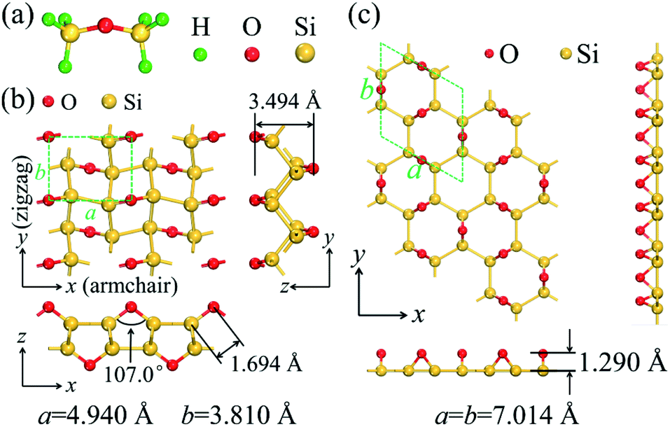 | ||
| Fig. 1 (a) The molecular structure of disilyl ether. Top and side views of the optimized structure of (b) silicether and (c) P6mm-Si2O. The dashed lines represent the corresponding primitive cells. | ||
To assess the relative stability of silicether, the cohesive energy is calculated as Ecoh = (mESi + nEO − Etotal)/(m + n), where ESi (EO) and Etotal are the total energies of an isolated Si (O) atom and a primitive cell, respectively. m (n) is the number of Si (O) atoms in the primitive cell. The cohesive energy of silicether is 6.19 eV per atom, much greater than that of silicene (∼3.4–4.0 eV per atom).29P6mm-Si2O has been identified as the most likely structure for the oxidation of silicene in an atmosphere of oxygen gas.14 However, its cohesive energy (5.91 eV per atom) is much smaller than that of silicether computed at the same level of theory, suggesting that silicether may be the most favourable structure for oxidized silicene with a Si![[thin space (1/6-em)]](https://www.rsc.org/images/entities/char_2009.gif) :O ratio of 2:1.
:O ratio of 2:1.
Next, we studied the phonon dispersion curves to assess the dynamical stability of silicether. The absence of imaginary frequencies in the phonon spectrum confirms the dynamic stability (Fig. 2a). The highest optical frequency reaches up to 800 cm−1, which is much larger than that in pristine silicene (∼550 cm−1),30 implying the strong covalent Si–O bonding. Furthermore, the thermal stability of silicether is tested by performing AIMD simulations on a relatively large 4 × 4 × 1 supercell. The time-dependent evolution of total energies oscillates within a very narrow range, indicating that silicether can maintain its structural integrity at 750 K (Fig. 2b). In addition, the structure is disrupted after ∼0.3 ps at 1000 K (Fig. S1†), which reveals that the melting point of silicether may be between 750 and 1000 K.
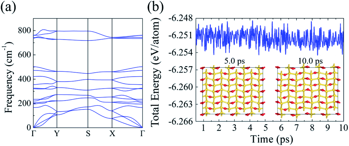 | ||
| Fig. 2 (a) Phonon dispersion of silicether. (b) Evolution of the total energies and snapshots for silicether at 750 K. | ||
As is well known, the instability of silicene, mainly because of its reaction with O2, greatly hinders the development of practical silicene-based devices. Thus, it is critical to examine the stability of silicether under ambient conditions. We carry out the AIMD simulation at 300 K for silicether exposed in O2 molecules. As shown in Fig. S2,† the structural integrity is perfectly maintained after 10 ps, and O2 molecules keep away from the surface of silicether without dissociating into oxygen atoms.
3.2. Electronic structures
After confirming the stabilities of silicether, we wonder whether it has a high band gap as well as high carrier mobility. Fig. 3a illustrates the band structure and the corresponding projected density of states (PDOS). Clearly, both the PBE and HSE06 results show that silicether is an indirect band gap semiconductor with both the conduction band minimum (CBM) and valence band maximum (VBM) locating between the Γ and X points. The indirect band gap (1.89 eV) is very close in energy with respect to the direct one (1.99 eV) at the HSE06 level. This weakly indirect band gap feature might be beneficial for light-emitting devices because of a very small change of electron momentum during the transition. The band gap is evidently wider than that of P6mm-Si2O (0.3 eV) but narrower than that of the fully oxidized silicene (2.1–5.1 eV from the PBE calculations).14 The moderate band gap is comparable to the ideal band gap for solar cell materials (∼1.4 eV),31 indicating that silicether has great potential for photovoltaic applications.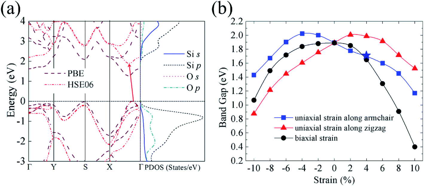 | ||
| Fig. 3 (a) Band structure and PDOS of silicether. (b) Band gap of silicether under the uniaxial and biaxial strain calculated by the HSE06 functional. The star indicates the direct band gap feature, and others represent the indirect band gap features. | ||
Moreover, the PDOS display the valence band mainly derived from the Si-3s3p and O-2p orbitals. The strongly overlapping of these orbitals in a broad energy range suggests the robust covalent bonding nature of the Si–Si and Si–O bonds. Moreover, from the charge densities of the VBM (Fig. S3†), we can see that the VBM state is mostly derived from the Si-3p and O-2p orbitals. The neighbouring Si–Si σ bonds are obviously overlapped. The delocalization of σ electrons originates from the charge transfer from oxygen lone electron pairs to σ*-antibonding orbitals of the Si–Si bonds, which is referred to as the hyperconjugation effect.
One of the most common methods to modulate the electronic properties of 2D materials is strain engineering.32–34 In addition, the structural deformations inevitably arise in material growth due to the lattice mismatch between the 2D layer and the substrate. As presented in Fig. 3b, the band gap of silicether shows a parabolic behaviour when applying uniaxial or biaxial strain. Under the uniaxial strain along the zigzag (armchair) direction, the band gap increases first and then decreases rapidly with increasing strain. This trend is similar to that of silicane with the application of uniaxial strain.35,36 On the other hand, the band gap of silicether exhibits a decreasing trend under the biaxial strain. It decreases to 0.41 eV at 10% of biaxial strain, which is of the same order of magnitude as that of the partially hydrogenated silicene (0.12 eV) under the biaxial strain of 12%.37 Moreover, the uniaxial tensile strain along the armchair direction can trigger an indirect–direct–indirect band gap transition (Fig. S4†). The potential direct band gap feature may be of interest in silicon-based light emitting devices.
To obtain insight into the nature of the indirect–direct–indirect band gap transition, we analyze the variation of the VBM and CBM states under uniaxial strain. The VBM located between the X and Γ points is mainly composed of Si (O)-py orbitals, but the CBM predominantly consists of Si-pxpz orbitals. The more px orbitals suggest that the CBM is more sensitive to the strain along the x (armchair) direction. Thus, the CBM experiences a faster change rate than the VBM. Both the VBM and CBM are situated at the same k-point under the 4% strain. As the strain continues to increase, the locations of VBM and CBM become different again. The sensitivities of different states to the uniaxial strain play a dominating role in the indirect–direct–indirect band gap transition.
3.3. Carrier mobilities
The carrier mobility of 2D materials has a great effect on the performance of electronic devices. The charge transport of silicether is estimated by using the acoustic-phonon-limited scattering model (see the ESI for details).38–40 The calculated deformation-potential constant, in-plane stiffness, effective mass, and carrier mobility are summarized in Table 1. From the band structure of silicether, the top of the valence band and the bottom of the conduction band are more dispersive along the Γ–X direction compared to the rather flat bands along the Γ–Y direction. Therefore, the carrier effective masses in the zigzag direction are an order of magnitude smaller than that in the armchair direction (Table 1). Furthermore, the in-plane stiffness values are anisotropic. In the zigzag direction, the in-plane stiffness of silicether is comparable to that of silicene (50–62 N m−1),41 while it becomes double in the armchair direction, suggesting the strong Si–O or Si–Si bond strength in silicether.| Carrier type | C 2D (N m−1) | E DP (eV) | m* (m0) | μ (cm2 V−1 s−1) |
|---|---|---|---|---|
| Electron (armchair) | 107.8 | 1.42 | 1.39 | 1.2 × 10³ |
| Hole (armchair) | 0.75 | 2.96 | 70 | |
| Electron (zigzag) | 57.4 | 0.56 | 0.34 | 6.4 × 10³ |
| Hole (zigzag) | 5.58 | 0.26 | 345 |
The calculated carrier mobilities show strong anisotropy. The electron (hole) mobility along the zigzag direction is about five times larger than that along the armchair direction. In addition, the electron mobility is significantly larger than the hole mobility. The marked difference between the electron and hole mobilities is favourable for electron–hole separation. Although the largest electron mobility (6.4 × 103 cm2 V−1 s−1) is smaller than that of silicene (2.6 × 105 cm2 V−1 s−1),42 it is much larger than that of black phosphorene (600–1580 cm2 V−1 s−1),43 MoS2 (72–201 cm2 V−1 s−1),44 and other predicted SOs (2–490 cm2 V−1 s−1).14 This suggests that the hyperconjugation effect plays an important role in enhancing the carrier mobility.
3.4. Optical properties
The band gap of silicether (1.89 eV) is close to that of cubic α-CsPbI3 (1.73 eV) which is a promising material for the top cell in organic–inorganic halide perovskite solar cells.45 To assess its light-harvesting performance, we calculate the in-plane and out-of-plane absorption coefficients (Fig. 4). The maximum in-plane absorption coefficient occurs at ∼270 nm, corresponding to the ultraviolet region. Moreover, in the visible light region, silicether also shows sizeable absorption coefficients (103–104 cm−1), indicating its potential in photovoltaic applications. On the other hand, the out-of-plane absorption coefficients can reach up to ∼105 cm−1 around 150 nm. In contrast to MoS2,46 the narrow absorption peak for silicether centered at 150 nm is favourable to developing ultraviolet light sensors.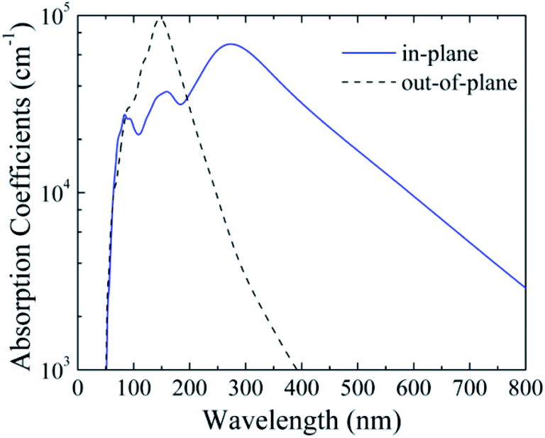 | ||
| Fig. 4 Calculated in-plane and out-of-plane absorption coefficients of silicether with the HSE06 method. | ||
3.5. Bilayer structures
Stacking is also an effective strategy to tune the electronic properties of 2D materials.47–49 Here we consider four possible stacking types of bilayer silicether, namely, AA-, AB-, AC-, and AD-stacking (Fig. S5†). As shown in Table 2, for the different stacking orders, the lattice constants (a and b) differ slightly. The most difference among the four stacking orders is the interlayer distance, which ranges from 1.643 Å in the AA-stacking to 3.121 Å in the AB-stacking. The AA-stacking is the most energetically stable, which shows the largest binding energy. The calculated binding energy of bilayer graphene (−25.82 meV Å−2) at the same level of theory is of the same order of magnitude as that of bilayer silicether. In contrast to the strong covalent interlayer bonding formed in bilayer silicene, the weak interlayer interaction in silicether layers indicates that the foreign O atoms effectively passivate the silicon network.50 Moreover, compared with monolayer silicether, bilayers have narrower band gaps. However, the indirect gap nature is preserved irrespective of the stacking order (Fig. S6†).| Stacking pattern | Lattice parameter (Å) | d z (Å) | E b (meV Å−2) | Band gap (eV) | |
|---|---|---|---|---|---|
| a | b | ||||
| AA | 9.858 | 7.626 | 1.643 | −30.64 | 1.55 |
| AB | 9.873 | 7.625 | 2.355 | −14.71 | 1.66 |
| AC | 9.878 | 7.604 | 2.191 | −20.66 | 1.60 |
| AD | 9.874 | 7.610 | 3.121 | −8.82 | 1.72 |
3.6. Potential synthesis mechanism
On the synthesis mechanism of silicether, one may wonder whether it could be formed by the assembly of precursor molecules. Thus, we investigated the adsorption and dehydrogenation of disilyl ether on Ag(100) as the initial stage of silicether growth.Various sites as well as different molecular orientations have been considered to confirm the stable adsorption site of disilyl ether (Fig. S7†). The disilyl ether adsorbed on the bridge site is the most stable configuration with the adsorption energy of 0.71 eV, in which the O atom is located on top of an Ag atom and two Si atoms lie above the midpoint between the two adjacent Ag atoms. The nearest Ag–O bond length is 3.072 Å, smaller than the sum of their vdW radii (4.08 Å).51 Therefore, the interaction between disilyl ether and Ag(100) is stronger than the vdW force. Furthermore, the DOS of the disilyl ether/Ag system could be viewed as a superposition of the ones of the two contributing isolated systems (Fig. S8†). Since there is no significant orbital hybridization, the covalent interaction between disilyl ether and Ag substrate is rather weak. The Hirshfeld charge analysis shows the charge transfer (∼0.3e) from the bottom Ag atom to the oxygen atom, indicating that the electrostatic interaction plays an important role in the disilyl ether adsorption.
In addition, the length of the Si–H bond is 1.492–1.503 Å, which is ∼0.01 Å larger than that in the free disilyl ether. In contrast, the Si–O bond length remains almost invariable, suggesting that the Si–O bond is difficult to break at the initial stage. As a result, the Ag(100) surface may be beneficial for disilyl ether dehydrogenation rather than dissociation.
We then investigate the dehydrogenation process of disilyl ether on Ag(100). The final product we considered is a SiOSi radical plus six H atoms on the surface. As shown in Fig. 5, there are eight intermediates in the reaction network. The structures of these intermediates and transition states for each elementary dehydrogenation step are plotted in Fig. S9.† All dehydrogenation steps are endergonic with the reaction energies in the range of 0.23–0.78 eV. Based on the activation barriers and reaction energies, we highlight the optimal pathway. The highest activation barrier along the optimal pathway is 1.02 eV, smaller than that of methane (∼2.0 eV)52 and coronene (1.87 eV)53 on Cu(111). During the six dehydrogenation steps, the reaction energy firstly increases from 0.23 eV to 0.74 eV and then decreases to 0.56 eV. Overall, the final product is 2.95 eV higher in energy than the initial state, suggesting that the complete dehydrogenation for disilyl ether is energetically unfavourable. Therefore, the partially dehydrogenated species will coalesce before going to the final hydrogen-free product. Silicether nucleation could be a continuous SixHyOz aggregation process and the full dehydrogenation occurs at a very late stage.
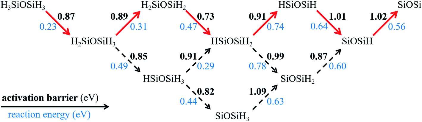 | ||
| Fig. 5 Activation barriers and reaction energies of the dehydrogenation network for disilyl ether on Ag(100). The reaction energy is defined by the difference between the Gibbs free energies of the product and reactant. The solid arrows highlight the optimal pathway. | ||
3.7. Exfoliation
Finally, to check the feasibility of isolating the silicether monolayer, we calculate the cleavage energy from a four-layer slab (Fig. 6). The total energy increases with the separation distance, reaching convergence at about 8 Å. The calculated exfoliation energy is 0.65 J m−2, which is larger than that of graphite (0.32 ± 0.03 J m−2) but of the same order of magnitude. Therefore, the monolayer could be isolated from few-layer silicether sheets via mechanical cleavage or liquid phase exfoliation.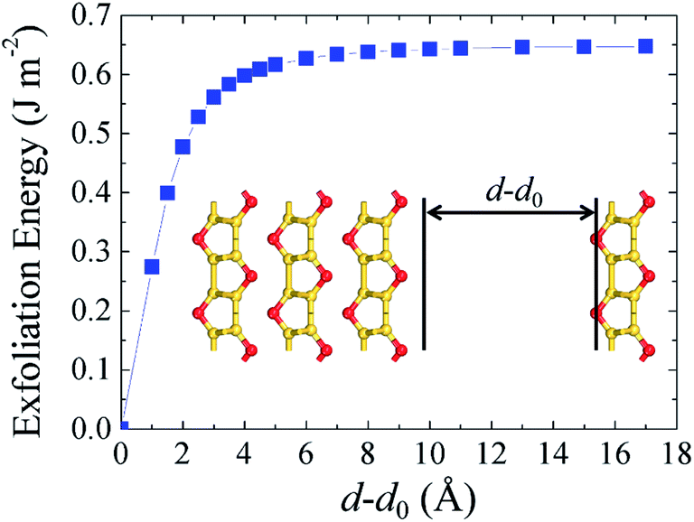 | ||
| Fig. 6 Calculated exfoliation energy with respect to the separation distance d–d0, where d0 represents the interlayer distance in the four-layer system. | ||
4. Conclusions
To summarize, we have designed a silicether monolayer via assembly of disilyl ether molecules, which has an indirect band gap (1.89 eV). An indirect–direct–indirect transition can be triggered under uniaxial strain. With unique hyperconjugation effects, silicether possesses high electron mobility (6.4 × 103 cm2 V−1) and in-plane stiffness (107.8 N m−1). Moreover, it shows excellent light harvesting ability in the ultraviolet-visible light region. Silicether bilayers also possess sizable band gaps with an indirect band gap characteristic due to the weak interlayer interaction. The successive dehydrogenation steps of disilyl ether on Ag(100) have the activation barriers lower than 1.02 eV, thus requiring moderate temperatures for this process. All these appealing properties make silicether a promising candidate for nanoelectronic and photovoltaic applications. We believe that our study will stimulate the design of 2D materials with hyperconjugated effects.Conflicts of interest
The authors declare no competing financial interests.Acknowledgements
This work was supported by the National Natural Science Foundation of China (grant no. 61974068 and 11704198) and the Summit of the Six Top Talents Program of Jiangsu Province (grant no. 2015-XCL-022).References
- J. Zhao, H. Liu, Z. Yu, R. Quhe, S. Zhou, Y. Wang, C. Cheng, H. Zhong, N. Han, J. Lu, Y. Yao and K. Wu, Prog. Mater. Sci., 2016, 83, 24–151 CrossRef CAS.
- P. Vogt, P. De Padova, C. Quaresima, J. Avila, E. Frantzeskakis, G. Le Lay, M. C. Asensio, A. Resta, B. Ealet and G. L. Lay, Phys. Rev. Lett., 2012, 108, 155501 CrossRef PubMed.
- N. D. Drummond, V. Zólyomi and V. I. Fal'ko, Phys. Rev. B: Condens. Matter Mater. Phys., 2012, 85, 075423 CrossRef.
- R. Quhe, R. Fei, Q. Liu, J. Zheng, H. Li, C. Xu, Z. Ni, Y. Wang, D. Yu, Z. Gao and J. Lu, Sci. Rep., 2012, 2, 853 CrossRef PubMed.
- L. Tao, E. Cinquanta, D. Chiappe, C. Grazianetti, M. Fanciulli, M. Dubey, A. Molle and D. Akinwande, Nat. Nanotechnol., 2015, 10, 227–231 CrossRef CAS PubMed.
- L. Chen, C. C. Liu, B. Feng, X. He, P. Cheng, Z. Ding, S. Meng, Y. Yao and K. Wu, Phys. Rev. Lett., 2012, 109, 056804 CrossRef PubMed.
- C. C. Liu, W. Feng and Y. Yao, Phys. Rev. Lett., 2011, 107, 076802 CrossRef PubMed.
- G. Li, L. Zhang, W. Xu, J. Pan, S. Song, Y. Zhang, H. Zhou, Y. Wang, L. Bao, Y.-Y. Zhang, S. Du, M. Ouyang, S. T. Pantelides and H.-J. Gao, Adv. Mater., 2018, 30, 1804650 CrossRef PubMed.
- L. Huang, Y.-F. Zhang, Y.-Y. Zhang, W. Xu, Y. Que, E. Li, J.-B. Pan, Y.-L. Wang, Y. Liu, S.-X. Du, S. T. Pantelides and H.-J. Gao, Nano Lett., 2017, 17, 1161–1166 CrossRef CAS PubMed.
- C.-C. Liu, W. Feng and Y. Yao, Phys. Rev. Lett., 2011, 107, 076802 CrossRef PubMed.
- A. Molle, C. Grazianetti, L. Tao, D. Taneja, M. H. Alam and D. Akinwande, Chem. Soc. Rev., 2018, 47, 6370–6387 RSC.
- M. Ali, Z. Ni, S. Cottenier, Y. Liu, X. Pi and D. Yang, J. Mater. Sci. Technol., 2017, 33, 751–757 CrossRef.
- R. Wang, M.-S. Xu and X.-D. Pi, Chin. Phys. B, 2015, 24, 086807 CrossRef.
- R. Wang, X. Pi, Z. Ni, Y. Liu, S. Lin, M. Xu and D. Yang, Sci. Rep., 2013, 3, 3507 CrossRef PubMed.
- M. Lundie, Ž. Šljivančanin and S. Tomić, J. Mater. Chem. C, 2015, 3, 7632–7641 RSC.
- D. Cremer, J. S. Binkley, J. A. Pople and W. J. Hehre, J. Am. Chem. Soc., 1974, 96, 6900–6903 CrossRef CAS.
- E. A. V. Ebsworth, R. Taylor and L. A. Woodward, Trans. Faraday Soc., 1959, 55, 211–219 RSC.
- G.-L. Zhu, X.-J. Ye and C.-S. Liu, Nanoscale, 2019, 11, 22482–22492 RSC.
- M. D. Segall, P. J. D. Lindan, M. J. Probert, C. J. Pickard, P. J. Hasnip, S. J. Clark and M. C. Payne, J. Phys.: Condens. Matter, 2002, 14, 2717–2744 CrossRef CAS.
- J. P. Perdew, K. Burke and M. Ernzerhof, Phys. Rev. Lett., 1996, 77, 3865–3868 CrossRef CAS PubMed.
- A. Tkatchenko and M. Scheffler, Phys. Rev. Lett., 2009, 102, 073005 CrossRef PubMed.
- D. R. Hamann, M. Schlüter and C. Chiang, Phys. Rev. Lett., 1979, 43, 1494–1497 CrossRef CAS.
- S. Savrasov and D. Savrasov, Phys. Rev. B: Condens. Matter Mater. Phys., 1996, 54, 16487–16501 CrossRef CAS PubMed.
- J. Heyd, G. E. Scuseria and M. Ernzerhof, J. Chem. Phys., 2003, 118, 8207–8215 CrossRef CAS.
- O. A. Vydrov, J. Heyd, A. V. Krukau and G. E. Scuseria, J. Chem. Phys., 2006, 125, 074106 CrossRef PubMed.
- S. Nosé, J. Chem. Phys., 1984, 81, 511–519 CrossRef.
- W. G. Hoover, Phys. Rev. A, 1985, 31, 1695–1697 CrossRef PubMed.
- N. Govind, M. Petersen, G. Fitzgerald, D. King-Smith and J. Andzelm, Comput. Mater. Sci., 2003, 28, 250–258 CrossRef CAS.
- S. Cahangirov, H. Sahin, G. Le Lay and A. Rubio, Lecture Notes in Physics 2017, vol. 230, Springer, Cham Search PubMed.
- X.-J. Ge, K.-L. Yao and J.-T. Lü, Phys. Rev. B: Condens. Matter Mater. Phys., 2016, 94, 165433 CrossRef.
- T. Minemoto, Y. Hashimoto, W. Shams-Kolahi, T. Satoh, T. Negami, H. Takakura and Y. Hamakawa, Sol. Energy Mater. Sol. Cells, 2003, 75, 121–126 CrossRef CAS.
- Z. Dai, L. Liu and Z. Zhang, Adv. Mater., 2019, 31, 1805417 CrossRef CAS PubMed.
- Y. Sun and K. Liu, J. Appl. Phys., 2018, 125, 082402 CrossRef.
- H. Xie, T. Ouyang, É. Germaneau, G. Qin, M. Hu and H. Bao, Phys. Rev. B: Condens. Matter Mater. Phys., 2016, 93, 075404 CrossRef.
- L. C. Lew Yan Voon, E. Sandberg, R. S. Aga and A. A. Farajian, Appl. Phys. Lett., 2010, 97, 163114 CrossRef.
- H. B. Shu, S. D. Wang, Y. H. Li, J. Yip and J. L. Wang, J. Chem. Phys., 2014, 141, 064707 CrossRef PubMed.
- W. C. Wu, Z. M. Ao, C. H. Yang, S. Li, G. X. Wang, C. M. Lie and S. Li, J. Mater. Chem. C, 2015, 3, 2593–2602 RSC.
- H. Lang, S. Zhang and Z. Liu, Phys. Rev. B: Condens. Matter Mater. Phys., 2016, 94, 235306 CrossRef.
- A. Rawat, N. Jena and A. De Sarkar, J. Mater. Chem. A, 2018, 6, 8693–8704 RSC.
- Y.-Q. Song, J.-H. Yuan, L.-H. Li, M. Xu, J.-F. Wang, K.-H. Xue and X.-S. Miao, Nanoscale, 2019, 11, 1131–1139 RSC.
- R. E. Roman and S. W. Cranford, Comput. Mater. Sci., 2014, 82, 50–55 CrossRef CAS.
- Z.-G. Shao, X.-S. Ye, L. Yang and C.-L. Wang, J. Appl. Phys., 2013, 114, 093712 CrossRef.
- J. Qiao, X. Kong, Z.-X. Hu, F. Yang and W. Ji, Nat. Commun., 2014, 5, 4475 CrossRef CAS PubMed.
- Y. Cai, G. Zhang and Y.-W. Zhang, J. Am. Chem. Soc., 2014, 136, 6269–6275 CrossRef CAS PubMed.
- W. Ahmad, J. Khan, G. Niu and J. Tang, Sol. RRL, 2017, 1, 1700048 CrossRef.
- H. Shi, H. Pan, Y.-W. Zhang and B. I. Yakobson, Phys. Rev. B: Condens. Matter Mater. Phys., 2013, 87, 155304 CrossRef.
- A. Azizi, G. Antonius, E. Regan, R. Eskandari, S. Kahn, F. Wang, S. G. Louie and A. Zettl, Nano Lett., 2019, 19, 1782–1787 CrossRef CAS PubMed.
- O. E. Parfenov, A. M. Tokmachev, D. V. Averyanov, I. A. Karateev, I. S. Sokolov, A. N. Taldenkov and V. G. Storchak, Mater. Today, 2019, 29, 20–25 CrossRef CAS.
- W. Zheng, B. Zheng, Y. Jiang, C. Yan, S. Chen, Y. Liu, X. Sun, C. Zhu, Z. Qi, T. Yang, W. Huang, P. Fan, F. Jiang, X. Wang, X. Zhuang, D. Li, Z. Li, W. Xie, W. Ji, X. Wang and A. Pan, Nano Lett., 2019, 19, 7217–7225 CrossRef CAS PubMed.
- T. Morishita and M. J. S. Spencer, Springer Series in Materials Science, 2016, vol. 235, Springer, Cham Search PubMed.
- S. S. Batsanov, Inorg. Mater., 2001, 37, 1031–1046 Search PubMed.
- W. Zhang, P. Wu, Z. Li and J. Yang, J. Phys. Chem. C, 2011, 115, 17782–17787 CrossRef CAS.
- X. Wan, K. Chen, D. Liu, J. Chen, Q. Miao and J. Xu, Chem. Mater., 2012, 24, 3906–3915 CrossRef CAS.
Footnotes |
| † Electronic supplementary information (ESI) available. See DOI: 10.1039/d0na00110d |
| ‡ The first two authors contributed equally to this work. |
| This journal is © The Royal Society of Chemistry 2020 |