
 Open Access Article
 This Open Access Article is licensed under a Creative Commons Attribution-Non Commercial 3.0 Unported Licence
A P/N type silicon semiconductor loaded with silver nanoparticles used as a SERS substrate to selectively drive the coupling reaction induced by surface plasmons
Yuanchun
Zhao
a,
Qijia
Zhang
a,
Liping
Ma
a,
Peng
Song
 *b and
Lixin
Xia
*ac
*b and
Lixin
Xia
*ac
aDepartment of Chemistry, Liaoning University, Shenyang 110036, P. R. China. E-mail: lixinxia@lnu.edu.cn
bDepartment of Physics, Liaoning University, Shenyang 110036, P. R. China. E-mail: songpeng@lnu.edu.cn
cYingkou Institute of Technology, Yingkou 115014, China
First published on 19th June 2020
Abstract
Semiconductor materials are favoured in the field of photocatalysis due to their unique optoelectronic properties. When a semiconductor is excited by external energy, electrons will transition through the band gap, providing electrons or holes for the reaction. This is similar to the chemical enhancement mode of a catalytic reaction initiated by the rough noble metal on the surface excited by plasmon resonance. In this study, different types of semiconductor silicon loaded with silver nanoparticles were used as SERS substrates. SERS detection of p-aminothiophenol (PATP) and p-nitrothiophenol (PNTP) probe molecules was performed using typical surface plasmon-driven coupling reactions, and the mechanism of optical drive charge transfer in semiconductor–metal–molecular systems was investigated. Scanning electron microscopy and plasmon luminescence spectroscopy were used to characterize the silver deposited on the substrate surface. Mapping technology and electrochemistry were used to characterize the photocatalytic reaction of the probe molecules. This study proposed a mechanism for the coupling reaction of “hot electrons” and “hot holes” on the surface of plasmon-driven molecules and provides a method for preparing a stable SERS substrate.
Introduction
In 1928, the Indian physicist Raman discovered that two colours of scattered light changed slightly when monochromatic light was used as a light source to observe scattered light – this phenomenon was called the Raman effect.1 The Raman effect is very weak because the scattered light intensity is only 10−10 times the intensity of incident light. Fleischmann et al. tested the single-molecule signal of pyridine molecules adsorbed on a rough silver electrode, which was 106 times higher than the signal in solution.2 Subsequent studies showed that this signal enhancement was due to the adsorption of molecules on the rough silver electrode surface. The signal enhancement of certain molecules is called Surface-Enhanced Raman Scattering (SERS).3,4 The electromagnetic enhancement (EM) and chemical enhancement mechanisms (CM) are two theories that describe SERS.5–10 The co-resonance of free electrons in a metal particle in a specific area under the action of incident light is called Local Surface Plasmon Resonance (LSPR).11,12 The EM mechanism is generally considered to be the detection of the SERS signal due to the enhancement of the electromagnetic field on the metal surface caused by the LSPR; whereas the CM mechanism is due to the charge transfer between the substrate and the molecule. In some systems, the CM and EM mechanisms are often complementary.13 Recent studies have shown that the reaction mechanisms of the typical surface plasmon induce the oxidation reaction of p-aminothiophenol (PATP), and the reduction reaction of p-nitrothiophenol (PNTP) to p-dimercaptoazobenzene (DMAB).14–18The quality of the SERS signal is closely related to the performance of the SERS substrate. Because the metal nanoparticles prepared by the sol method are easily clustered in solution, the reproduction performance in Raman spectroscopy is poor, and inexpensive and easily available semiconductor materials have also been tried as SERS substrate materials.19–22 Semiconductors are important catalyst components in the field of photocatalysis. The electron–hole pairs in a semiconductor are induced to transition by light and provided for the reaction. Compared with conventional photocatalytic performance, semiconductors undergo laser induced plasmon resonance. This not only allows electrons or holes to be better transported to its surface and greatly improves the material's ability to transport electrons, but also enhances the local photoelectric magnetic field on the surface to increase the formation of electron–hole pairs. The thermal effect of the process can also better promote the progress of the chemical reaction and is not limited to improving the selective enhancement of molecular signals.23–26
The enhancement effect of semiconductors as SERS substrates is not as obvious as that of metal nanoparticles such as gold and silver. In order to solve the problem of the stability and enhancement effect of the substrate, Lombardi dispersed silver nanoparticles on CuO films and used it as a SERS substrate. The probe molecules showed a good signal and stability and high reproducibility.27 As for the preparation method of the metal–semiconductor composite material, it is mainly based on a semiconductor self-assembly method, a sputtering method, a vapor deposition method, and a redox method. Recent research has focused on semiconductor–metal nanoparticle systems, such as Si/GaN–Au/Ag nanoparticles.28,29 In this system, the substrate morphology and synthesis process can affect the detection performance of SERS.18,30,31 Therefore, this paper provides a method for preparing SERS composite substrates with strong and reusable silicon semiconductor–silver nanoparticles synthesized by the self-assembly method, and analyses the regulation process of the electron (hole) caused by the optical drive charge transfer.
Experimental
Materials
PATP and PNTP were purchased from Aldrich Chemical Co. AgNO3 and NaSO4 were purchased from Energy Chemical. The samples were used without additional treatment. P-type silicon doped with boron, n-type silicon doped with phosphorus, and ordinary undoped intrinsic silicon wafers were purchased from Tuoxu Electronic Technology Co., Ltd. (Guangzhou, China). P-type silicon and n-type silicon were fully doped, the crystal orientation was <100>, resistivity was all 0.001–0.005 Ω cm, and since the intrinsic silicon is not doped, its resistivity is >1000 Ω cm. Sulfuric acid, hydrochloric acid, nitric acid, hydrofluoric acid, hydrogen peroxide, acetone, and ethanol were purchased from ANAGI Chemicals. All aqueous solutions used in the study were freshly prepared in Milli-Q water (>18 MΩ cm−1).Preparation of SERS substrates
P- type silicon, n-type silicon, and ordinary undoped intrinsic silicon wafers were cut into 1 cm × 2 cm (2 pieces each, 6 pieces in total), immersed in acetone solution for 10 min, rinsed with deionized water, and then placed in a piranha solution of H2O2![[thin space (1/6-em)]](https://www.rsc.org/images/entities/char_2009.gif) :H2SO4 (1:4) for 10 min to remove organic matter from the surface. After washing with deionized water, the silicon wafers were placed in 5% hydrofluoric acid for 5 min to remove surface oxides before dilution with deionized water for termination. After washing with deionized water and drying with nitrogen, the silicon wafers were washed again with ethanol and water before being dried by nitrogen. They were then placed vertically in 10 mM AgNO3 containing 5% hydrofluoric acid, and silver was deposited for 10 minutes under UV light at a wavelength of 365 nm. After removing from UV light after 10 minutes, the silicon wafers were rinsed with 10 mM HCl.
:H2SO4 (1:4) for 10 min to remove organic matter from the surface. After washing with deionized water, the silicon wafers were placed in 5% hydrofluoric acid for 5 min to remove surface oxides before dilution with deionized water for termination. After washing with deionized water and drying with nitrogen, the silicon wafers were washed again with ethanol and water before being dried by nitrogen. They were then placed vertically in 10 mM AgNO3 containing 5% hydrofluoric acid, and silver was deposited for 10 minutes under UV light at a wavelength of 365 nm. After removing from UV light after 10 minutes, the silicon wafers were rinsed with 10 mM HCl.
After SEM characterization of the obtained substrates, the substrates were immersed in 10−3 M PATP or 10−3 M PNTP solutions for 30 min and then completely dried for SERS detection (Scheme 1). The Mott–Schottky curve of the substrate was tested with an electrochemical workstation before and after the reaction. The carrier concentration change value and its flat band potential were calculated before and after the reaction, and the positions of the conduction band and valence band were derived. Based on density functional theory (DFT), the highest occupied molecular orbital (HOMO) and lowest unoccupied molecular orbital (LUMO) were calculated, and the photo-induced charge transfer model between the semiconductor–metal–molecule was studied.
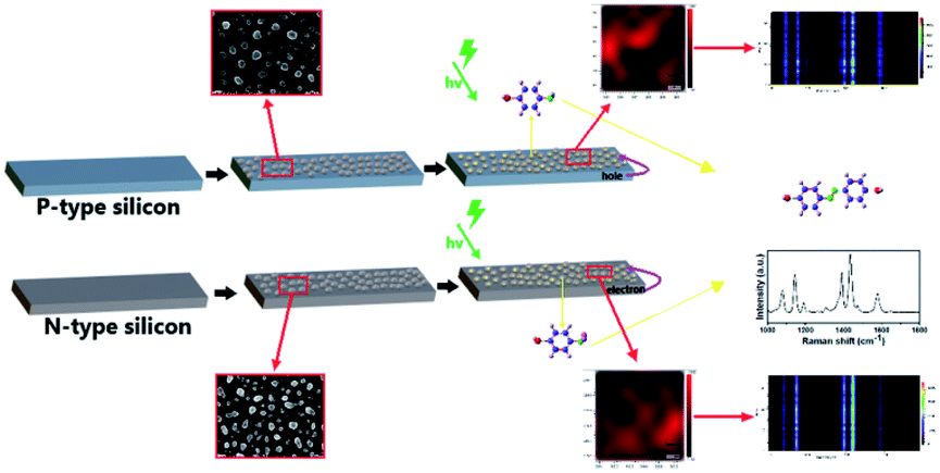 | ||
| Scheme 1 Description of the SERS mechanism used to detect probe molecules on silicon substrates of different doping types. | ||
Material characterization
Scanning electron microscopy was performed with a JEOL JSM-7400F SEM at an operating voltage of 15 kV. The Raman spectrum was measured with an inVia Raman spectrometer (Renishaw Trading Co., Ltd.). Among them, PATP and PNTP-related Raman detection used a laser with a wavelength of 532 nm for excitation and an exposure time of 10 seconds. Since under the catalysis of plasmons, the reduction reaction of the nitro group had better SERS sensitivity compared with the oxidation reaction of the amino group.18 The SERS signal, for which the probe molecule was PATP, was detected at 2.5 mV (PNTP, 0.5 mV). Mapping technology was used to randomly select 36 points, and a green light source with an excitation wavelength of 532 nm was used. The exposure time was 1 second (36 seconds in a row). The Mott–Schottky curve was obtained using a CHI660e electrochemical workstation (Shanghai Chenhua Instrument Co., Ltd., China), and the electrolyte solution was 0.5 M NaSO4. The silver nanoparticles on the substrate were dissolved with 5% nitric acid and analysed by inductively coupled plasmon luminescence spectroscopy (ICP, 7500A). X-ray photoelectron spectrometer (XPS) analysis was carried out using a Thermo Scientific ESCALAB 250 (150 W, spot size of 500 μm), and corrected according to the standard carbon peak 284.6 eV.Results and discussion
Morphological characterization of SERS substrates deposited under different conditions
Three types of silicon wafers (p-type silicon, n-type silicon, and ordinary undoped silicon wafers) were exposed to either dark conditions or UV irradiation. In the presence of hydrofluoric acid, the silver deposition occurred mainly from the following process:| Si + 6F− → SiF62− + 4e− |
| Ag+ + e− → Ag |
Fig. 1 shows SEM images of p-type silicon, n-type silicon and intrinsic silicon following exposure to dark conditions and UV irradiation. Among them, (a–c) are SEM images of silver nanoparticles deposited on p-type silicon, n-type silicon, and ordinary undoped high-resistance silicon wafers, respectively, under dark conditions; (d–f) are SEM images of silver nanoparticles deposited on the same three types of silicon wafers under UV light.
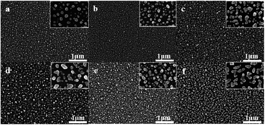 | ||
| Fig. 1 SEM characterization of silver nanoparticles deposited on different substrates under the two conditions. | ||
The three silicon wafers exposed to either condition showed extremely high uniformity. Under dark conditions, the silver deposited on the surface of p-type silicon and n-type silicon appeared as spherical particles with a diameter of approximately 60 nm, while the silver on the intrinsic silicon wafer appeared as irregular shapes with more intercept points, which could provide more “hot spots” in SERS detection. The results indicated that different silver nanoparticle morphologies can develop on different types of silicon substrates.32 Under UV light irradiation, the silver particle sizes increased. The silver nanoparticles deposited on the surface of p-type silicon and n-type silicon also showed irregular shapes with multiple intercept points. This indicated that UV light can affect the morphology of silver nanoparticles. In addition, the silver nanoparticles deposited on n-type silicon under UV light showed greater density. This is because the conduction band of n-type silicon had excess electrons. Under UV light, a large number of electrons transition to the surface and are directly provided to Ag+ for reduction reactions, and silver nanoparticles on an n-type silicon surface show greater density.33
In addition, we immersed the six substrates in 5% HNO3 for one hour, and then analysed the silver content on the substrate surfaces. The ICP test results are shown in Table 1. The contents of various substrates were consistent with the results shown in Fig. 1. The density of silver nanoparticles deposited on (d–f) under UV light is higher than that of silver in (a–c). The silver content of (e and f) is obviously higher than that of other bases. The high content of the (e) base is due to the excess electrons in the base itself. The high (f) content is due to the measurement error caused by the inconsistency in the cutting process of the silicon wafer.
| a | b | c | d | e | f | |
|---|---|---|---|---|---|---|
| Ag mg L−1 | 4.24 | 4.19 | 5.43 | 5.18 | 6.18 | 6.78 |
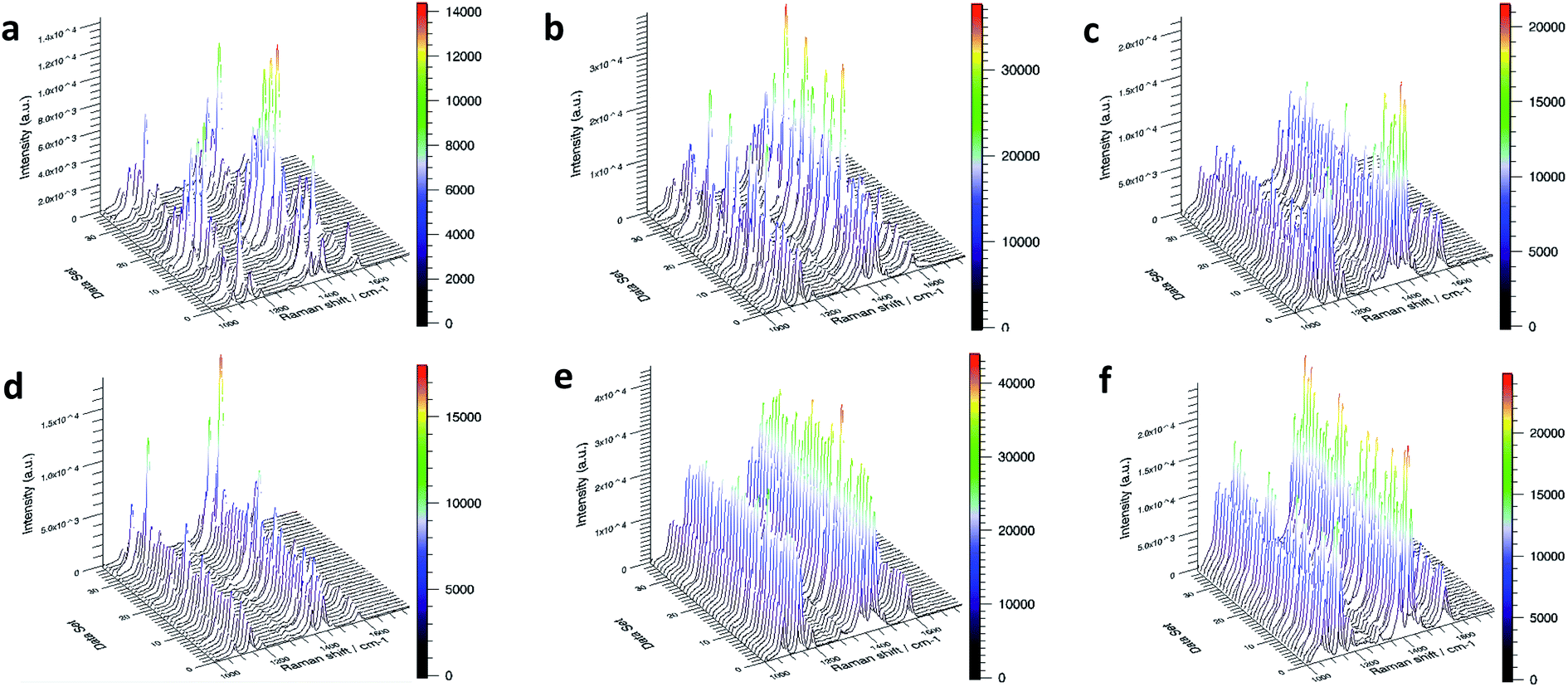
SERS signal analysis of PATP/PNTP molecules on different substrates
As shown in Fig. 2, we first measured the Raman spectra of powders PATP and PNTP to determine the peak location of the substance. And then, the six substrates were immersed in 10−3 M PATP or 10−3 M PNTP solution for 30 min. The SERS-based mapping results are shown in Fig. 3 (PATP) and 4 (PNTP). PATP undergoes a coupling reaction on all substrates to become DMAB.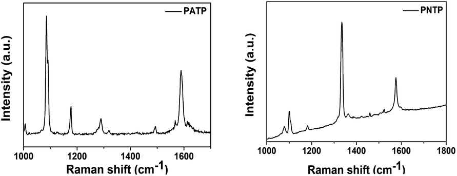 | ||
| Fig. 2 Raman spectra of PATP and PNTP powders. | ||
 | ||
| Fig. 3 Mapping analysis of PATP on different substrates by SERS. | ||
 | ||
| Fig. 4 Mapping analysis of PNTP on different substrates by SERS. | ||
The reaction on the ordinary intrinsic silicon wafer (Fig. 3c and f) showed a good signal-to-noise ratio because the silver nanoparticles deposited under both conditions had a rough 3D structure. For p-type silicon and n-type silicon substrates with the same resistivity, the comparison of the detection signals of PATP on different substrates showed that the SERS signal of the PATP reaction on p-type silicon was superior to that on n-type silicon.
The coupling reaction of PNTP to DMAB occurred on all substrates tested (Fig. 4). The reactions on the ordinary intrinsic silicon wafers (Fig. 4c and f) showed a good signal-to-noise ratio. Since the silver nanoparticles deposited under both conditions had a 3D rough structure and many hot spots, the reaction was considered to be effective. Comparing the reaction of PNTP on p-type silicon and n-type silicon, the SERS signal of the PNTP reaction on n-type silicon was better than that of p-type silicon, and the reaction on p-type silicon was not complete (Fig. 4). Substrates deposited with silver under UV light had a better SERS signal than under dark conditions. This is because silver nanoparticles produced LSPR absorption under 365 nm UV light, so they are stronger during SERS detection. The electromagnetic field produces a better SERS signal.
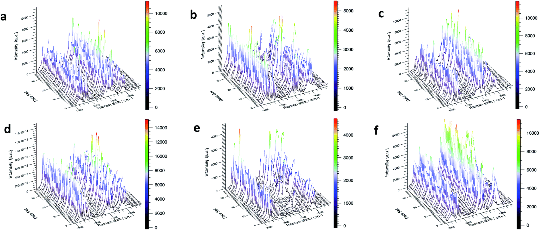
Based on the above experimental results, SERS signals of different enhanced factors could be obtained from PATP and PNTP on different bases. According to the mapping detection diagram in Fig. 3 and 4, the corresponding spectral analysis diagram is drawn, as shown in Fig. 5. Among them, (a–f) is the morphology of silver nanoparticles on different substrates; the second row is the spectrum analysis diagram based on SERS of PATP on each substrate, and the third row is the spectrum analysis diagram of PNTP. By comparing Fig. 3 with Fig. 5, it can be seen that in the reaction on n-type silicon (bases b and e), the characteristic peaks of PATP at 1084 cm−1, 1176 cm−1, and 1616 cm−1 had not disappeared and are more obvious than those of the other two substrates. The characteristic peaks 1141 cm−1, 1389 cm−1, and 1429 cm−1 corresponding to DMAB were not continuous and weaker than those of the other two substrates, indicating that the reaction was not complete.34 Therefore, the enhanced factor of PATP SERS detection on n-type silicon was smaller than that on p-type silicon. Similarly, by comparing the Raman spectrogram of PNTP and the relative spectrogram based on SERS, it can be seen that the enhanced factor of SERS detection of PNTP on p-type silicon was smaller than that on n-type silicon.
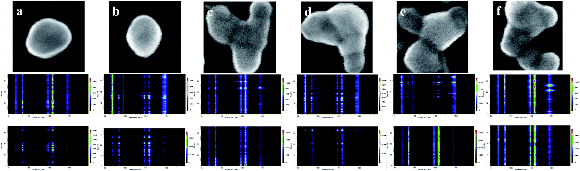 | ||
| Fig. 5 PATP and PNTP spectra on different substrates. | ||
Change of carrier concentration before and after the reaction in the substrate
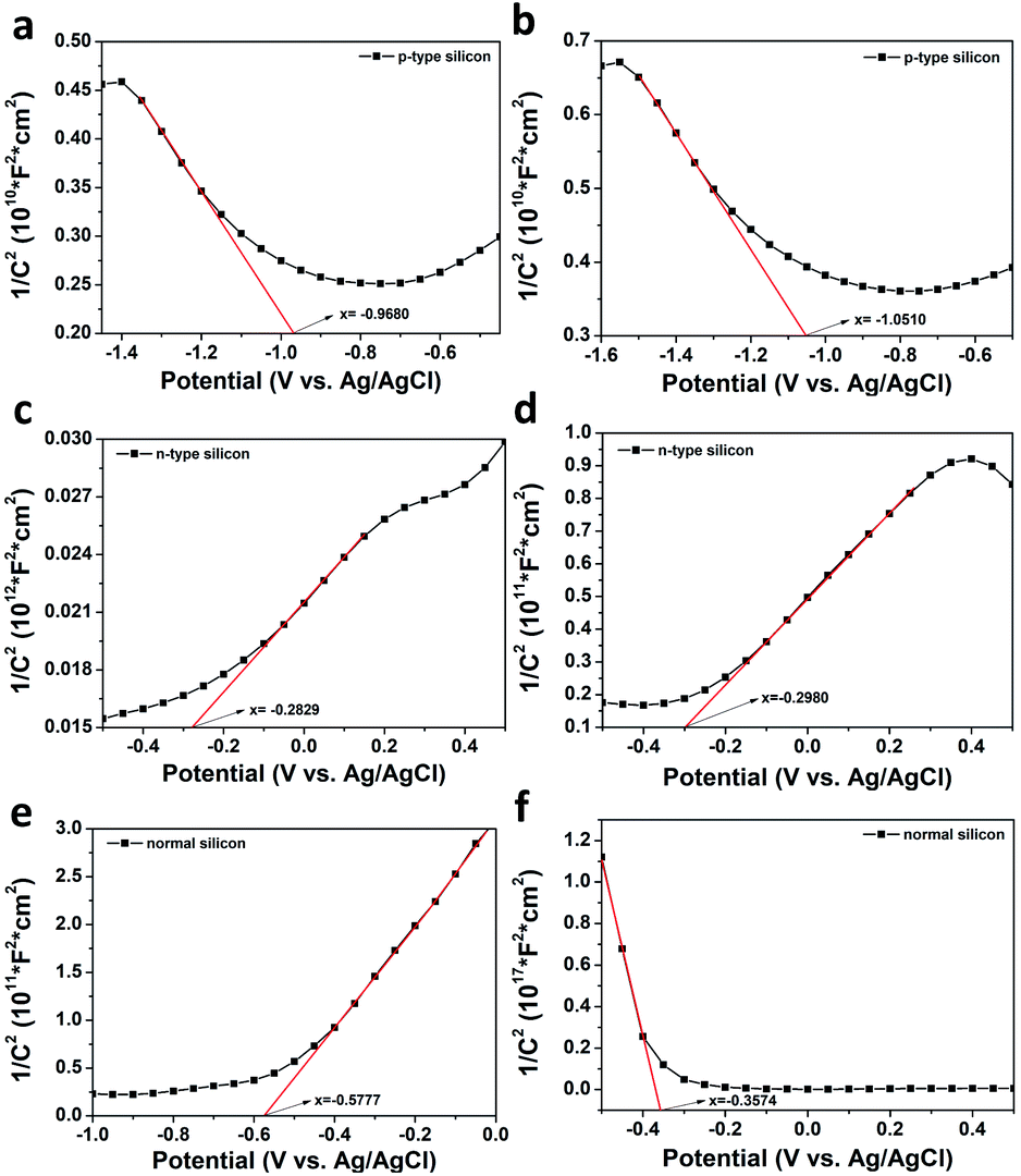
As shown above, the coupling reaction of the p-type silicon to the probe molecule PATP was more favourable. Similarly, the coupling reaction of the n-type silicon to the probe molecule PNTP was more favourable. Therefore, we hypothesised that during the reaction between PATP and PNTP, p-type silicon and n-type silicon provided holes and electrons to the reaction molecules, respectively.Based on the above, we studied the carrier concentration before and after the substrate reaction. The p-type silicon and n-type silicon substrates were irradiated by a 532 nm laser and the unreacted p-type silicon and n-type silicon were placed in 0.5 M NaSO4 electrolyte solution for a Mott–Schottky test.
Fig. 6 shows the Mott–Schottky measurement results of the silicon substrates before and after the reaction. Among them (a and b) are the Mott–Schottky curves measured before and after the reaction of the PATP molecules on the p-type semiconductor; (c and d) are the Mott–Schottky curves measured before and after the reaction of the PNTP molecules on the n-type semiconductor; (e and f) are Mott–Schottky curves measured after the reaction of PATP and PNTP molecules on the intrinsic semiconductor.
 | ||
| Fig. 6 Mott–Schottky test results on different substrates. | ||
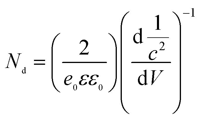
As shown in Fig. 6a–d, the measured slope of p-type silicon and n-type silicon substrates before and after the reaction did not change, but the flat band potential changed. The carrier concentration was calculated according to the following formula, as well as the slope and abscissa (Table 2), where e0 is the electronic charge, ε is the dielectric constant of silicon, and ε0 is the vacuum dielectric constant.
| Carrier concentration before reaction (cm−3) | Carrier concentration after reaction (cm−3) | |
|---|---|---|
| P-type silicon | 1.98 × 10¹⁹ | 1.56 × 10¹⁹ |
| N-type silicon | 0.62 × 10¹⁹ | 0.10 × 10¹⁹ |
The results showed that the carrier concentration of p-type silicon and n-type silicon decreased after the reaction, indicating that during the reaction, p-type silicon provides holes for the reaction of PATP, and n-type silicon provides it with electrons for the PNTP reaction. Based on this, we studied the reaction on an intrinsic silicon substrate. Fig. 6e and f show the Mott–Schottky curves of PATP and PNTP on the intrinsic silicon substrate measured after the reaction. Fig. 6e shows the characteristics of n-type semiconductors, indicating that the internal electron content was relatively high, which also explained the supply of holes during the reaction. In contrast, Fig. 6f shows the characteristics of the p-type semiconductor, indicating that the substrate provides electrons during the PNTP coupling reaction.
Principles of optical drive charge transfer for semiconductor–metal-probe molecules
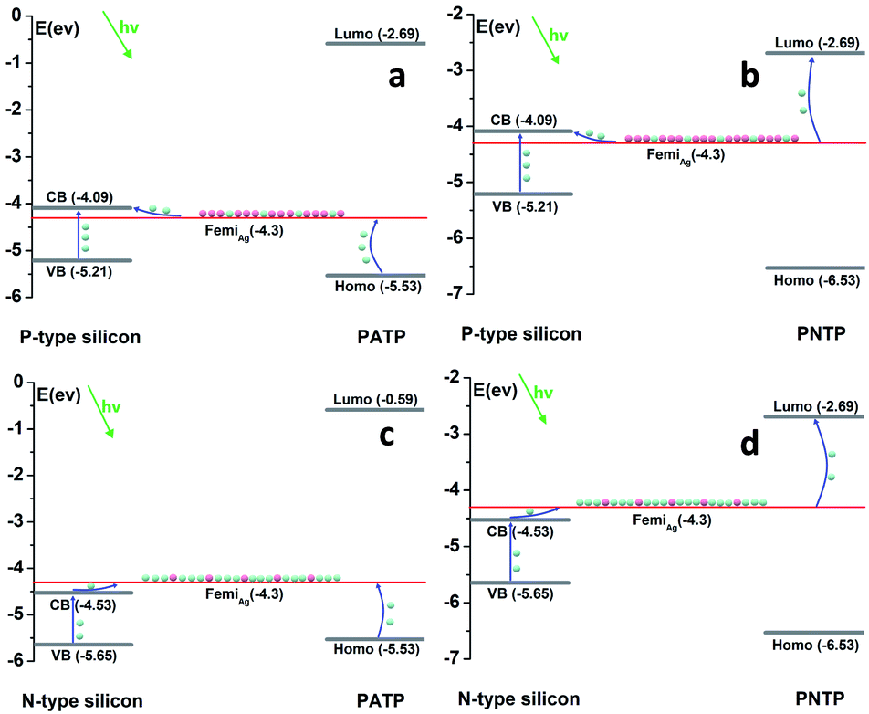
In the system of silicon–silver-probe molecules prepared by the above experiments, it is very unlikely that the semiconductor can directly provide electrons or holes to the probe molecule over the metal.35 Therefore, we believed that during the reaction, the laser excites the electrons or holes of the semiconductor to the surface of the silver nanoparticle, so that the surface of the silver nanoparticle is loaded with more electrons or holes for the reaction.We detailed the reaction mechanism of the system (Fig. 7). According to the flat band potential measured by the Mott–Schottky curve and the band gap of silicon, the conduction and valence band positions of the three silicon types were obtained. The flat band potential was converted according to the following formula, where the pH is 7 and the absolute electrode potential of the standard hydrogen electrode (SHE) is −4.44 eV, as specified by the International Union of Pure and Applied Chemistry (IUPAC).36 The Fermi level of silver is −4.3 eV, and the corresponding theoretical analysis was made according to the LUMO and HOMO values of PATP and PNTP molecules.37
| ERHE = EAg/Agcl + 0.059pH + E0Ag/Agcl |
 | ||
| Fig. 7 Light-induced charge transfer mechanism at the semiconductor–metal–molecule interface. The green spheres represent electrons and the red spheres represent holes. | ||
Fig. 7a shows a p-type semiconductor–silver–PATP molecular model. Excited by a laser with a wavelength of 532 nm, the electrons in the valence band of the p-type semiconductor transition to the conduction band. During the electronic transition, some of the electrons that belong to silver also transition to the semiconductor. PATP is oxidized by the loss of electrons. Under the catalysis of plasmons, the multi-electron HOMO calculated based on density functional theory needs to transfer electrons to the surface of silver to complete the oxidation reaction of PATP under the irradiation of a laser.37 Because some electrons are transferred to the semiconductor during the transfer process, the silver nanoparticles have a lower electron concentration, so they are more receptive to HOMO electrons, making the reaction more favorable. Similarly, for the p-type semiconductor–silver–PNTP molecular model shown in Fig. 7b, PNTP needs to gain electrons in order to obtain the reduced product. Under laser induction, molecular LUMOs need to capture electrons from the silver surface in order to complete the reduction reaction of the nitro group. In this state, the silver nanoparticle has a low electron concentration, and it is difficult for the electronic transition from the Fermi level to the LUMO to occur. Likewise, for the n-type semiconductor–silver–PATP molecular model, the electrons in the valence band begin to guide the band transition upon laser induction, and the electrons transition to the silver to make the electron concentration on the silver surface higher. Due to the difference in concentration, the electrons in the LUMO of PATP are less likely to undergo a transition to the silver Fermi level. However, for the n-type semiconductor–silver–PNTP molecular model shown in Fig. 7, the electrons located at the silver Fermi level are more likely to make the transition to the HOMO level of the PNTP molecule. Therefore, p-type semiconductors are more prone to oxidation reactions involving amino groups, whereas n-type semiconductors have a driving effect on the reduction reactions of nitro groups.
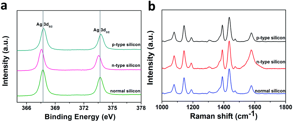
In order to confirm the above charge transfer mechanism, we carried out XPS tests on p-type silicon, n-type silicon and ordinary intrinsic silicon substrates deposited with silver nanoparticles. As shown in Fig. 8a, compared to the silver nanoparticles deposited on intrinsic silicon, the binding energy shift of the silver nanoparticles deposited on n-type silicon was smaller, indicating that the silver valence state on n-type silicon was slightly reduced. This result also demonstrated that a large number of electrons were loaded on the silver nanoparticles. Similarly, the displacement of silver on p-type silicon was larger, indicating that there were more holes on the surface of silver nanoparticles on p-type silicon.
 | ||
| Fig. 8 (a) XPS analysis of silver particles deposited on different substrates and (b) SERS signal detection performed on substrates prepared three months earlier. | ||
We also performed a SERS test on the substrate prepared three months earlier to test the stability of the SERS substrate. As shown in Fig. 8b, the signals of various substrates were of good quality, indicating a stable performance by the substrates.
Conclusions
In summary, this article not only provides a method for preparing electroless deposition of a SERS composite substrate with high activity and stability, but also showed that UV light affects the morphology of nanoparticles. In addition, the principle of optical drive charge transfer in semiconductor–metal–organic molecular systems was investigated. Combined with the results of theoretical calculations, the study demonstrated that the electrons or holes generated by P/N semiconductors under laser induction can achieve a selective coupling reaction of driving molecules.Conflicts of interest
There are no conflicts of interest to declare.Acknowledgements
This work was supported by the Shenyang High-Level Innovative Talents Program (Grant no. RC180227), the LiaoNing Revitalization Talents Program (Grant No. XLYC1807162), the National Natural Science Foundation of China (Grant No. 21671089 and 11974152), the Scientific Research Fund of Liaoning Province (Grant No. 2019-ZD-0487) and the Liaoning Provincial Department of Education Project (Grant No. LJC201904).Notes and references
- C. V. Raman and K. S. Krishnan, Nature, 1928, 121, 501–502 CrossRef CAS.
- M. Fleischmann, P. J. Hendra and A. J. Mcquillan, Chem. Phys. Lett., 1974, 26, 163–166 CrossRef CAS.
- D. L. Jeanmaire and R. P. V. Duyne, J. Electroanal. Chem. Interfacial Electrochem., 1977, 84, 1–20 CrossRef CAS.
- M. G. Albrecht and J. A. Creighton, J. Am. Chem. Soc., 1977, 99, 5215–5217 CrossRef CAS.
- J. Gersten and A. Nitzan, J. Chem. Phys., 1980, 73, 3023–3037 CrossRef CAS.
- D. A. Weitz, J. Chem. Phys., 1983, 78, 5324 CrossRef CAS.
- A. Otto, I. Mrozek, H. Grabhorn and W. Akemann, J. Phys.: Condens. Matter, 1992, 4, 1143–1212 CrossRef CAS.
- M. Moskovits, Rev. Mod. Phys., 1985, 57, 783–826 CrossRef CAS.
- J. Billmann and A. Otto, Solid State Commun., 1982, 44, 105 CrossRef CAS.
- J. R. Lombardi, R. L. Birke, T. Lu and J. Xu, J. Chem. Phys., 1986, 84, 4174–4180 CrossRef CAS.
- M. S. Yavuz, G. C. Jensen and D. P. Penaloza, Langmuir, 2009, 25, 13120–13124 CrossRef CAS PubMed.
- Y. W. Ma, Z. W. Wu and L. H. Zhang, Plasmonics, 2013, 8, 1351–1360 CrossRef CAS PubMed.
- J. R. Lombardi and R. L. Birke, J. Phys. Chem. C, 2008, 112, 5605–5617 CrossRef CAS.
- H. Wang, T. Liu and Y. Huang, Sci. Rep., 2014, 4, 7087 CrossRef CAS PubMed.
- Y. F. Huang, M. Zhang, L. B. Zhao, J. M. Feng and D. Y. Wu, Angew. Chem., Int. Ed., 2014, 53, 2385–2389 CrossRef.
- D. Y. Wu, M. Zhang, L. B. Zhao, Y. F. Huang, B. Ren and Z. Q. Tian, Sci. China: Chem., 2015, 58, 574–585 CrossRef CAS.
- L. Kang, P. Xu and B. Zhang, Chem. Commun., 2013, 49, 3389 RSC.
- Y. C. Zhao, H. C. Zhang, P. Song and L. X. Xia, Plasmonics, 2020, 15, 31–37 CrossRef CAS.
- P. Dimitrios, D. Angeliki and A. Petros, Nanoscale, 2019, 11, 21542–21553 RSC.
- Q. Tao, J. Dong and W. Qian, Progress in Chemistry, 2013, 25, 1031–1041 CAS.
- X. Li, Y. Shang and J. Lin, Adv. Funct. Mater., 2018, 28, 1870228 CrossRef.
- Y. Wang, W. Ruan and J. Zhang, J. Raman Spectrosc., 2009, 40, 1072–1077 CrossRef CAS.
- S. Fateixa, H. I. S. Nogueira and T. Trindade, Phys. Chem. Chem. Phys., 2015, 17, 21046–21071 RSC.
- S. A. Belhout, F. R. Baptista and S. J. Devereux, Nanoscale, 2019, 11, 19884–19894 RSC.
- L. Brus, Acc. Chem. Res., 2008, 41, 1742–1749 CrossRef CAS PubMed.
- K. Watanabe, D. Menzel and N. Nilius, Chem. Rev., 2006, 106, 4301–4320 CrossRef CAS PubMed.
- Y. Wang, W. Song and W. Ruan, et al. , J. Phys. Chem. C, 2009, 113, 8065–8069 CrossRef CAS.
- M. Kosović, M. Balarin and M. Ivanda, Appl. Spectrosc., 2015, 69, 1417–1424 CrossRef PubMed.
- N. Mhlanga, T. Domfe and A. Skepu, Appl. Surf. Sci., 2019, 476, 1108–1117 CrossRef CAS.
- J. Guo, S. Xu and X. Liu, Appl. Surf. Sci., 2016, 396, 1130–1137 CrossRef.
- A. B. Sagyndykov, Z. K. Kalkozova and G. S. Yar-Mukhamedova, Tech. Phys., 2017, 62, 1675–1678 CrossRef CAS.
- A. Lahiri, R. Wen and S. Kuimalee, CrystEngComm, 2012, 14, 1241–1246 RSC.
- R. Wang, D. Liu and Z. Zuo, J. Mater. Chem., 2012, 22, 2410 RSC.
- M. T. Sun, Z. Zhang and H. Zheng, Sci. Rep., 2012, 2, 647 CrossRef.
- X. Y. Wang, D. K. Parrish, J. A. Malen and K. L. P. Chan, Sci. Rep., 2015, 5, 16095 CrossRef CAS PubMed.
- W. A. Donald, R. D. Leib and M. Demireva, J. Am. Chem. Soc., 2009, 131, 13328–13337 CrossRef CAS PubMed.
- L. B. Zhao, Y. F. Huang and X. M. Liu, Phys. Chem. Chem. Phys., 2012, 14, 12919 RSC.
| This journal is © The Royal Society of Chemistry 2020 |