
 Open Access Article
 This Open Access Article is licensed under a Creative Commons Attribution-Non Commercial 3.0 Unported Licence
The dual interfacial modification of 2D g-C3N4 for high-efficiency and stable planar perovskite solar cells
Zhou
Liu
ab,
Shuzhen
Wu
ab,
Xiaojie
Yang
ab,
Yijun
Zhou
ab,
Jiaren
Jin
ab,
Junmei
Sun
c,
Li
Zhao
 *ab and
Shimin
Wang
*ab
*ab and
Shimin
Wang
*ab
aHubei Collaborative Innovation Center for Advanced Organic Chemical Materials, Wuhan 430062, PR China. E-mail: zhaoli7376@163.com
bMinistry-of-Education Key Laboratory for the Green Preparation and Application of Functional Materials, Faculty of Materials Science and Engineering, Hubei University, Wuhan 430062, P. R. China
cCollege of Pharmacy and Biological Engineering, Chengdu University, Chengdu 610106, P. R. China
First published on 13th October 2020
Abstract
Carrier recombination and charge loss at the interfaces of perovskite layers have a significant influence on high-performance planar perovskite solar cells (PSCs). We employed two-dimensional graphitic carbon nitride (g-C3N4), which is a heat-resistant n-type semiconductor, to modify the electron-transport layer/perovskite and perovskite/hole-transport layer interfaces, respectively. g-C3N4 could passivate the surface trap states of the methylammonium lead iodide light absorber through the formation of a Lewis adduct between N and the under-coordinated Pb, and it could also remarkably reduce the grain boundaries between perovskite crystal particles. A maximum power conversion efficiency (PCE) of 19.67% (Voc = 1.14 V, Jsc = 21.45 mA cm−2, FF = 0.807) could be obtained from planar PSCs with long-term stability using dual-positioned g-C3N4. Therefore, we consider that ultrathin semiconductor films with a Lewis base nature are suitable as dual-functional transport materials for devices. This work provides new guidance for dual-interfacial modification to improve the PCE and stability of devices.
1. Introduction
Organic–inorganic lead halide perovskite solar cells (PSCs) have attracted extensive attention because of their outstanding photovoltaic and optical properties, such as long charge carrier diffusion lengths, strong optical absorption, and low electron–hole recombination rates.1–6 Therefore, the power conversion efficiency (PCE) of these devices has increased from 3.9% to 25.2% over the past few years.7–11 However, trap states have a great influence on PSC performance, which limits the ability of PSCs to obtain theoretical PCE of >30%.12Currently, four main defects exist on the surface of perovskite layer: (1) halide vacancies bringing about uncoordinated Pb2+ defects (2); Pb–I anti-site or halide excess; (3) cation vacancies (FA+ and MA+); (4) metallic lead.13–22 Energy disorder and obstruction of charge extraction are caused by the surface of perovskite layer defects as interfacial non-radiative recombination centers, which will result in a lower fill factor (FF), smaller open-circuit voltage (Voc), and a sharply decreased PCE.23–25 Hence, interfacial modification is helpful to optimize perovskite films because it alters the interface of the perovskite layer to reduce defects.26 For example, Mohamadkhani et al. reported planar PSCs with CdS modification at the perovskite/SnO2 electron transport layer (ETL) interface, which achieved a PCE of 17.18%.27 Luo et al. showed devices with interfacial modification by thiourea to obtain a PCE of 19.18%.28 However, the complex defects in polycrystalline perovskite films (grain boundaries, pinholes, and crystal defects) are inevitable at the perovskite/hole transport layer (HTL) interface. Li et al. studied devices grown with the polymer poly(4-vinylpyridine) (PVP) at the perovskite/HTL interface, and an average PCE of 18.95% was obtained.29 Wang et al. introduced planar PSCs based on a multifunctional ammonium salt at the perovskite/HTL interface to yield an optimum PCE of 18.95% and a steady-state output PCE of 18.11%.30 Nevertheless, these methods solve only one problem, which is not conducive to gaining higher FF and short-circuit current density (Jsc).31–35 Thus, it is necessary to find a material to modify at ETL/perovskite and perovskite/HTL interfaces.36 Dual interfacial modification is conducive to reducing defects while passivating defects.
In this work, we used g-C3N4 to modify the interfaces of ETL/perovskite and perovskite/HTL, respectively. A several layer-thick or monolayer-thick g-C3N4 have been shown to be outstanding two-dimensional (2D) nanomaterials in optoelectronics and electronics thanks to their excellent tunable optoelectronic properties and high chemical and thermal stability.37–43 Although g-C3N4 modification does not exhibit desirable band alignments among ETL, HTL, and MAPbI3 perovskite absorbers at the two interfaces, an observably increased PCE of 19.69% for g-C3N4 dual-incorporated PSCs over the pristine device (PCE = 18.03%) has been obtained.44 This result is principally because g-C3N4 can reduce trap density dramatically at ETL/perovskite and perovskite/HTL interfaces.
2. Experimental section
2.1 Materials
Perovskite (PbI2, MAI) and HTL ((spiro-MeOTAD, lithium-bis(tri-fluoromethanesulfonyl)imide (Li-TFSI), and (4-tert-butylpyridine (tBP)) solutions were purchased from Xi'an Polymer Light Technology. Dimethyl sulfoxide (DMSO) (99.9%) and 4-hydroxybutyric acid lactone (DMF) (99.9%) were purchased from Sigma-Aldrich and Aladdin, respectively. SnCl2·2H2O (98%) and urea (99.9%) were purchased from Alfa Aesar.2.2 Device fabrication
The F-doped SnO2 substrate was cleaned by using deionized water, isopropyl alcohol, ethanol, and isopropyl alcohol, respectively. The F-doped SnO2 substrate was irradiated by UV-ozone for 15 min before deposition of SnO2 ETLs. The solution of SnO2 precursor was spin-coated on glass at 4000 rpm for 30 s, and then annealed for 10 min at 180 °C. The g-C3N4 precursor was spin-coated on an SnO2 film at 4000 rpm for 30 s, and then annealed for 5 min at 100 °C. A MAPbI3 perovskite solution (1.3 M) was spin-coated on top of the g-C3N4 layer at 1000 rpm for 6 s and 4000 rpm for 30 s. During spinning, 100 μL of chlorobenzene was dropped onto the spinning perovskite film for 16 s. Then, the films were annealed for 10 min at 100 °C. The g-C3N4 precursor was spin-coated on top of the perovskite layer at 4000 rpm for 30 s, and then annealed for 5 min at 100 °C. Then, 20 μL of spiro-OMeTAD solution containing 36.1 mg of spiro-OMeTAD, 14.4 μL of t-BP, 9 μL of Li-TFSI solution (520 mg in acetonitrile) and 500 μL of chlorobenzene was spin-coated on the g-C3N4 layer at 4000 rpm for 30 s. Finally, Au of thickness 50 nm was deposited by thermal evaporation.
2.3 Device characterization
Absorbance was recorded with a UV-vis spectrophotometer (UV-3600; Shimadzu). The X-ray diffraction (XRD) patterns of samples and perovskite films were measured with an AXS D8 advance system (Bruker). The morphology of MAPbI3 perovskite films was measured with a scanning electron microscope (500 series; Sigma). g-C3N4 particles were characterized via transmission electron microscopy (TEM) using a G2 F20 system (Tecnai). The incident photo-to-electron conversion efficiency (IPCE) of PSCs was analyzed using a 300 W xenon lamp (66984; Newport). The photocurrent–voltage (J–V) characteristics of PSCs were analyzed under simulated AM 1.5 G radiation (irradiance of 100 mW cm−2) using a solar simulator (91192-1000; Oriel) and a source meter (2400; Keithley). Electrochemical impedance spectroscopy (EIS) was employed using an electrochemical workstation (IM6; Zennium) over a frequency range of 100 mHz to 2 MHz with 10 mV AC amplitude at −1 V bias under simulated AM 1.5 G radiation (irradiance of 100 mW cm−2). Devices were measured under ambient conditions [15% < relative humidity (RH) < 60%] each time (winter or summer). After measurements had been taken, devices were stored in a humidity-controlled dry room (15% < RH < 40%).3. Results and discussion
A schematic diagram of g-C3N4 dual-modified PSCs is displayed as Fig. 1. We fabricated a typical planar PSC configuration of FTO/SnO2/MAPbI3/spiro-OMeTAD/Au. The other layers were coated by spin-coating except that Au was deposited by thermal evaporation. The upper and lower layers of perovskite were modified by multilayer g-C3N4. Lone-pair electrons on g-C3N4 could usefully coordinate unreacted lead ions at the perovskite/HTL interface, which could reduce the surface defects of the perovskite layer and improve the photoelectric performance of devices. Meanwhile, g-C3N4 could reduce the Gibbs free energy of the SnO2 surface to serve as nucleation centers for perovskite growth and promote the nucleation process of perovskites at the ETL/perovskite interface. The porous structure of g-C3N4 also strengthened the contact between the perovskite layer and HTL and ETL, respectively.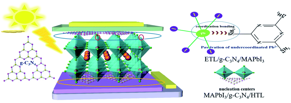 | ||
| Fig. 1 g-C3N4 dual-modified PSCs (schematic diagram). | ||
The XRD pattern of samples obtained after urea had been treated at high temperature is shown in Fig. 2(a). The intense diffraction peak at 27.5° was assigned to the (002) crystal plane of g-C3N4 (JCPDS-87-1526).45 g-C3N4 was a typical polymer semiconductor in which the C–N atoms were sp2 hybrid orbitals to form a highly delocalized conjugated system and electron-donor group. Covalent bonds were formed by the 6p empty orbit in under-coordinated Pb2+ and the lone pair electrons on C–N atoms, which helped to reduce the surface defects of the perovskite layer. A lower concentration of defects could increase the transportation and extraction of charge carriers. Fourier transform infrared (FTIR) spectroscopy of g-C3N4 was used to analyze absorption bonds. Peaks at ∼3363 cm−1 and ∼3362 cm−1 represent –NH2 bending vibrations (Fig. 2(b)). Peaks at ∼800 cm−1 and 1200–1650 cm−1 represent the stretching vibration of the triazine units and C–N heterocycle. g-C3N4 had several N–H groups, which could passivate the defects of the perovskite layer effectively and improve the PCE of PSCs. The optical changes of MAPbI3 perovskite films with and without g-C3N4 dual-positioned at both interfaces were evaluated (Fig. 2(c)). Dual interfacial modification (g-C3N4) could help the perovskite films to gain absorbance in the absorption range 350–750 nm. This result showed that the perovskite layer had good crystallinity, which would enhance Jsc of PSCs. We also obtained the XRD of the samples of SnO2 ETLs interface-modified with and without g-C3N4 (Fig. 2(d)). The characteristic peaks of MAPbI3 at 14.5° and 28.5° corresponded to the (110) and (220) crystal planes, respectively. The enhanced diffraction peak intensities showed that perovskite crystallization improved after g-C3N4 modified SnO2 ETLs.
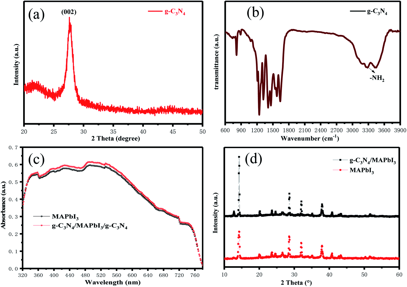 | ||
| Fig. 2 (a) The XRD pattern of g-C3N4 film. (b) The FTIR spectrum of g-C3N4 film. (c) UV-vis absorption spectra of SnO2/MAPbI3 and SnO2/g-C3N4/MAPbI3/g-C3N4 films. (d) XRD patterns of MAPbI3 and g-C3N4/MAPbI3 films. | ||
Fig. 3(a) shows the TEM image of pure g-C3N4 particles: a multi-layer sheet-like morphology with smooth surface was observed.46 We adopted dynamic spin-coating during the experiment, which was good for thinner and smoother g-C3N4 films. The top-view SEM images exhibited in Fig. 3(b) and (c) demonstrate that MAPbI3 perovskite film grown on SnO2/g-C3N4 exhibited a larger average particle size than that of perovskite on pristine SnO2. The enlarged grains could be attributed to g-C3N4 with hydrophobic and low surface-restraining perovskite nucleation. SEM revealed that g-C3N4 obviously reduce the number of surface defects and grain boundaries. The size of layer-built g-C3N4 materials covered on perovskite films was from several nanometers to ∼10 nm (Fig. 3(d)). Defects of perovskite grain boundaries are usually caused by loss of intergranular atoms, disordered arrangement or bond distortion, which leads to accumulation, serious trapping, and recombination of charge carriers. Small-scale g-C3N4 nanoparticles can effectively passivate defects at grain boundaries of the MAPbI3 film surface by forming strong hydrogen bonds between MA+ and N atoms, which enhances charge extraction and suppresses carrier recombination.
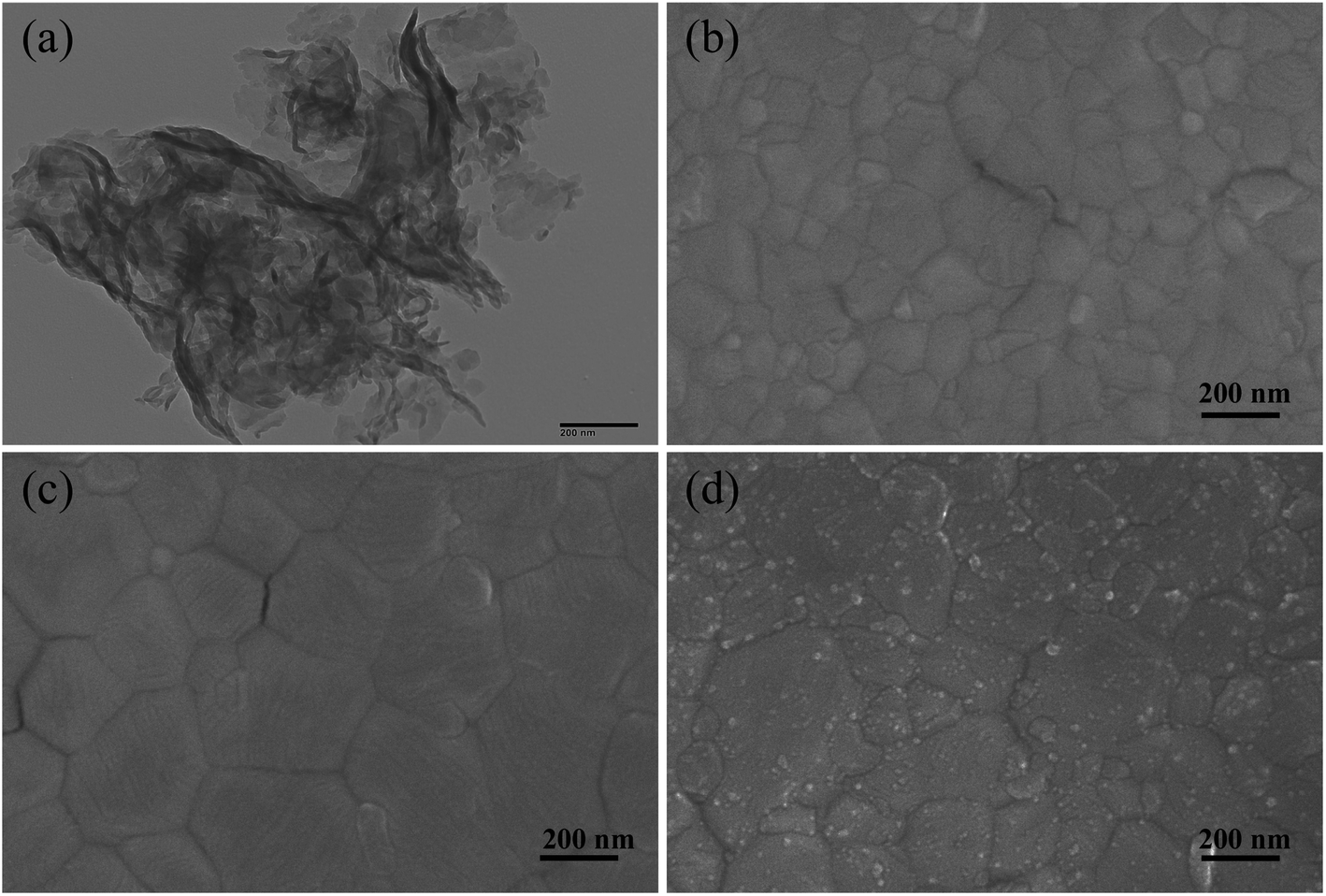 | ||
Fig. 3 (a) A TEM image of pure g-C3N4. (b–d) Top-view SEM images of planar PSCs with and without g-C3N4-modified SnO2 ETLs and a planar PSC with g-C3N4 simultaneously modifying the SnO2 ETL and perovskite-layer (50![[thin space (1/6-em)]](https://www.rsc.org/images/entities/char_2009.gif) 000×). 000×). | ||
Fig. 4(a) demonstrates the photovoltaic characteristics of typical PSCs (0.06 cm−2) and one with a g-C3N4-modified MAPbI3 perovskite absorber at the two interfaces under AM 1.5 G irradiation at 100 mW cm−2. The control device showed a PCE of 18.03% with Voc of 1.12 V, Jsc of 20.3 mA cm−2 and FF of 0.793. By contrast, the champion device with g-C3N4 dual positions exhibited a Jsc of 21.45 mA cm−2, Voc of 1.14 V, and FF of 0.807 and, thus, a much higher PCE of 19.67%. Dual-interface treatment led to an increase in Voc from 1.12 to 1.14 V, of Jsc from 20.30 to 21.45 mA cm−2, and of FF from 0.793 to 0.807. The increase in Voc and FF could have been because g-C3N4 modified at the perovskite/HTL interface reduced the surface defects of perovskite films. g-C3N4 modified at the ETL/perovskite interface increased the absorption of the perovskite layer, which resulted in an increase in Jsc. The external quantum efficiency (EQE) spectra of devices and the one with g-C3N4 dual-positioned at both interfaces are sketched in Fig. 4(b). The EQE responses of the two champion devices exhibited high photon current conversion efficiency (75–90%). The integrated current value counted from the IPCE spectra was 20.59 and 21.17 mA cm−2, respectively. Compared with the pristine device, the IPCE spectra of the devices with g-C3N4 dual-incorporation increased significantly. These consequences were consistent with the corresponding best short-circuit current density, which demonstrated that the emission of our solar simulator was in accordance with the spectrum. IPCE = LHE × φinj × ηcc, where LHE is the light-harvesting efficiency, φinj is the electron-injection efficiency, and ηcc is the charge-collection efficiency.47 Hence, a better device with g-C3N4 dual-incorporation will have stronger light absorption and charge transport.
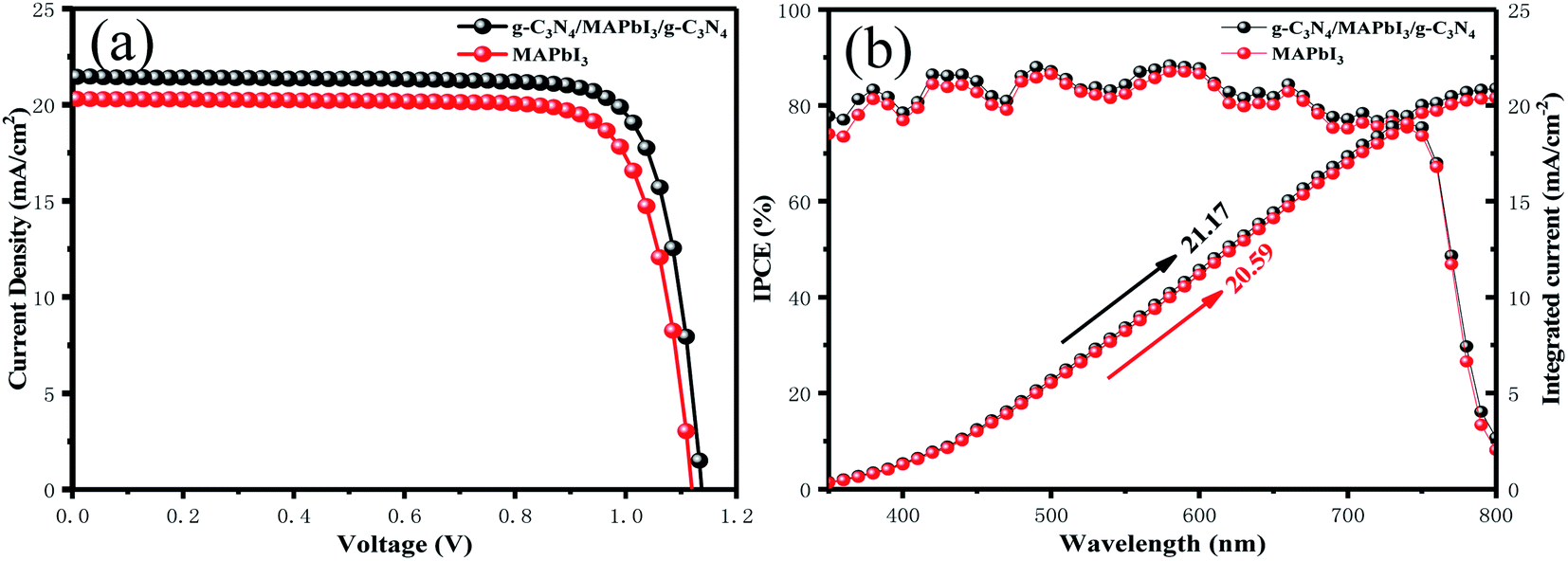 | ||
| Fig. 4 (a) J–V curves of a pristine planar PSC and a planar PSC with g-C3N4 simultaneously modifying the SnO2 ETL and perovskite layer. (b) IPCE spectra of a pristine device and a device with g-C3N4-modified interfaces (ETL/g-C3N4/perovskite/g-C3N4/spiro-OMeTAD). | ||
Devices with and without g-C3N4 dual-positioned at both interfaces and statistical analyses of the key photovoltaic parameters (PCE, FF, Voc, and Jsc) are shown in the inset of Fig. 5(a)–(d). Pristine PSCs displayed a mean PCE of 17.46 ± 0.57%, mean Voc of 1.11 ± 0.02 V, mean Jsc of 20.33 ± 0.32 mA cm−2, and mean FF of 0.772 ± 0.021. The photovoltaic parameters of the g-C3N4 dual-modified PSCs were all higher than those of pristine devices because the PSCs could bring about an enhanced mean PCE of 19.1 ± 0.68%, mean Voc of 1.13 ± 0.02 V, mean Jsc of 21.31 ± 0.32 mA cm−2, and mean FF of 0.793 ± 0.024. The photovoltaic parameters of the devices and the one with g-C3N4 dual modifications are summarized in Table 1. Based on the analyses mentioned above, we think that ultrathin semiconductor films based on the property of Lewis bases are suitable for dual-modification at the two interfaces of the perovskite layer. Consequently, the device with g-C3N4 dual-incorporation at both interfaces performed best.
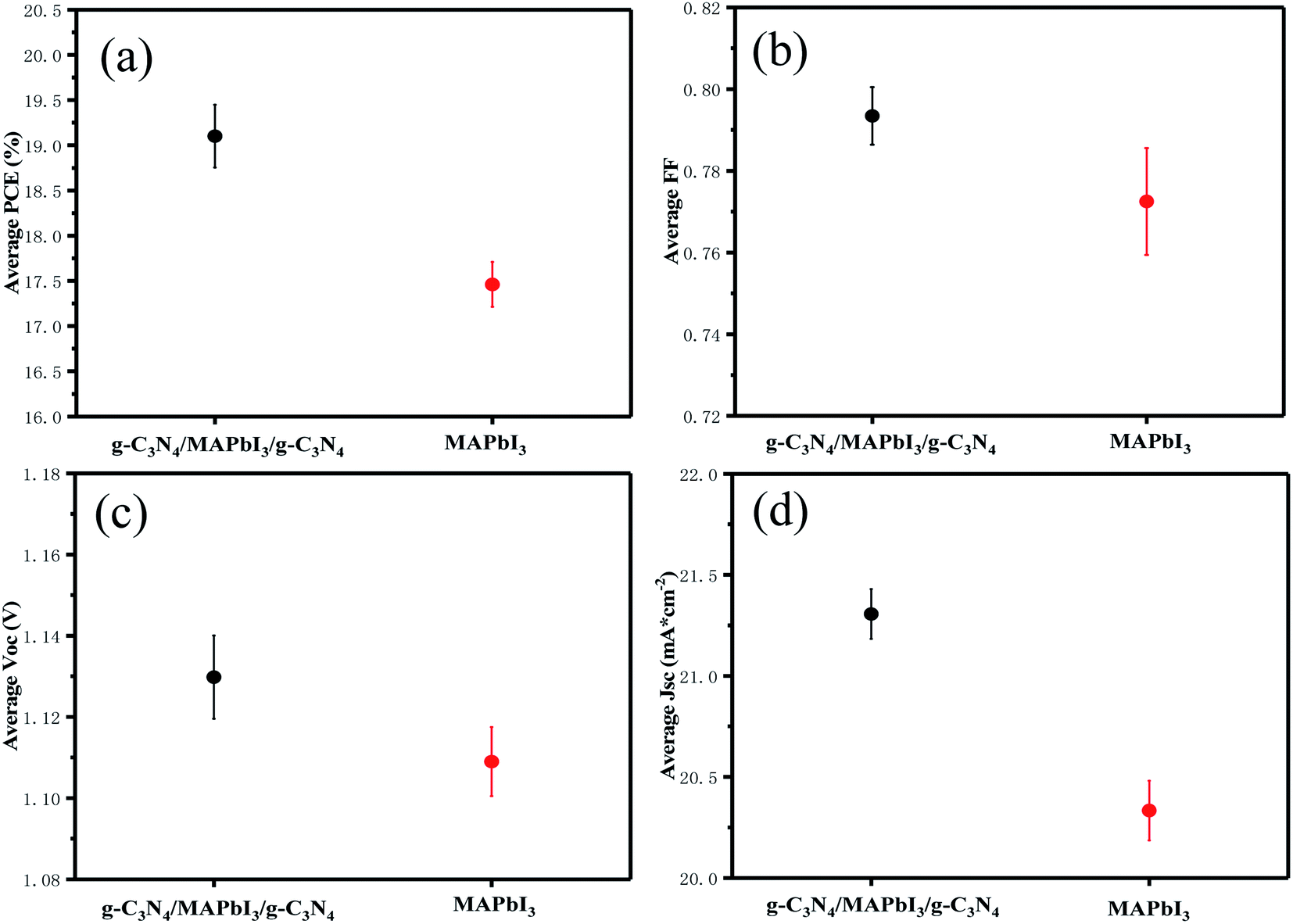 | ||
| Fig. 5 Statistical analyses of (a) PCE, (b) FF, (c) Voc, and (d) Jsc efficiency values, using 10 devices to calculate each value. | ||
| PSC | V oc (V) | J sc (mA cm−2) | FF | PCE (%) | Highest PCE (%) |
|---|---|---|---|---|---|
| Standard | 1.11 ± 0.02 | 20.33 ± 0.32 | 0.772 ± 0.021 | 17.46 ± 0.57 | 18.03 |
| Modified | 1.13 ± 0.02 | 21.31 ± 0.32 | 0.793 ± 0.024 | 19.1 ± 0.68 | 19.67 |
A photoluminescence (PL) quenching experiment was used to analyze charge-transfer kinetics. More efficient PL-quenching of perovskite films upon g-C3N4 dual-incorporation than that of pristine perovskite films are depicted in Fig. 6(a). PL quenching was due to enhancement in extraction of charge carriers across the interface at the ETL/perovskite and perovskite/HTL interfaces with g-C3N4 dual positions. Enhanced interfacial contact conductivity can lead to a reduction in charge accumulation and can improve the injection and transportation of electrons. The charge-transport behavior of devices with and without g-C3N4 dual-incorporation was studied further using time-resolved photoluminescence (TR-PL) spectra (Fig. 6(b)). A bi-exponential decay function could fit the PL decay time, and corresponded to a slow radiative decay and a fast radiative decay in perovskite materials. Table 2 lists all the important parameters. For the pristine sample, the fast decay time (τ1) was 116.9 ns, and the slow decay time (τ2) was 31.47 ns, with an amplitude τave (τave = ΣAiτi2/ΣAiτi, where A1 and A2 are pre-exponential factors) of 56.06 ns. Compared with the pristine perovskite, τ1 was 99.5 ns, and τ2 was 28.01 ns, and resulted in an amplitude τave of 46 ns. The average lifetime of the g-C3N4 dual-incorporated device decreased sharply, which is beneficial for suppressing charge recombination and increasing the number of photon-induced electrons and hole transfer at the ETL/perovskite and perovskite/HTL interfaces, respectively. Hence, FF and Jsc were enhanced markedly, a finding that was consistent with the J–V and IPCE (Fig. 4(a) and (b)) measurement.
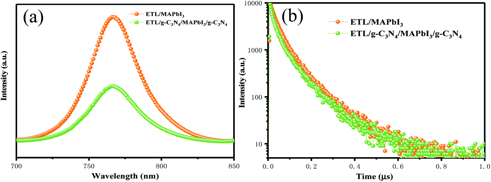 | ||
| Fig. 6 (a) Steady-state PL spectra of PSCs with and without g-C3N4 dual-incorporation. (b) Time-resolved PL spectra of PSCs with and without g-C3N4 dual-incorporation. | ||
| PSC | τ 1 (ns) | τ 2 (ns) | τ ave (ns) |
|---|---|---|---|
| SnO2/MAPbI3 | 116.9 | 31.47 | 56.06 |
| SnO2/g-C3N4/MAPbI3/g-C3N4 | 99.5 | 28.01 | 46 |
For the interpretation of the effect of g-C3N4 dual-modified devices on charge recombination, we measured EIS within the frequency range of 10 mHz to 2 MHz at −1 V bias under dark conditions. The Nyquist plots of the devices with and without g-C3N4 dual-incorporation are shown in Fig. 7. The latter shows the equivalent circuit containing a recombination resistance (Rrec), chemical capacitance (C), and series resistance (Rs). A smaller Rs of 11.31 Ω for the device with g-C3N4 dual-positioned than that of the pristine device (Rs = 15.26 Ω) indicated enhanced conductivity. The devices had a much lower Rs with a relatively higher FF. A larger Rrec of 716.2 Ω for the device with g-C3N4 dual modifications than that of the pristine device (Rrec = 413.8 Ω) showed more efficient charge dissociation and transport. As a consequence, the boosted charge transfer relieved the loss in interfacial charge, thereby contributing to increase Voc (Voc = Eg/q − Vloss) and Jsc.
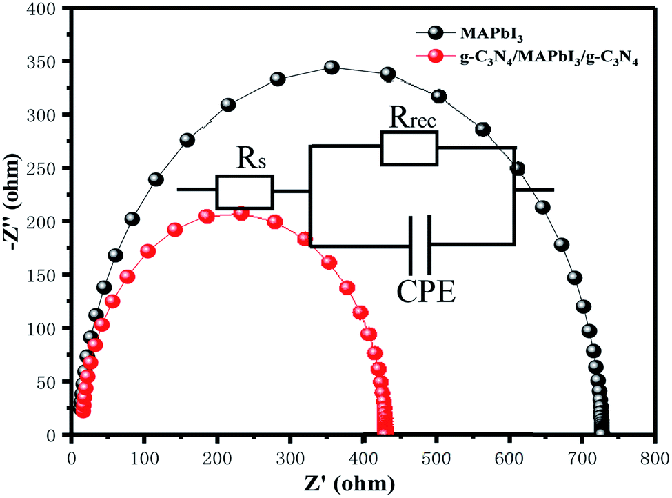 | ||
| Fig. 7 Nyquist plots of PSCs with and without g-C3N4-modified interfaces (ETL/g-C3N4/perovskite/g-C3N4/spiro-OMeTAD). | ||
Fig. 8 shows the steady-state output at the maximum power point (MPPT) under the constant bias voltages and AM 1.5 G illumination measured. Champion devices with and without g-C3N4 dual-incorporation were biased at 0.97 and 0.89 V, respectively. In a continuous measurement for 200 s, the g-C3N4 dual-incorporated device achieved a stabilized efficiency of 19.2%, which was superior to that of the pristine device (17.32%). High values of MPPT and biasing voltage could have been because g-C3N4 reduced the surface defects of perovskite films while passivating defects. The surface defects of the perovskite layer and trapped charge can give rise to the migration of iodide and ion mobilization within perovskite lattices, which eventually affect PSC stability. Therefore, the highly stable PCE of PSCs explained how the g-C3N4 dual interface reduced defects significantly.
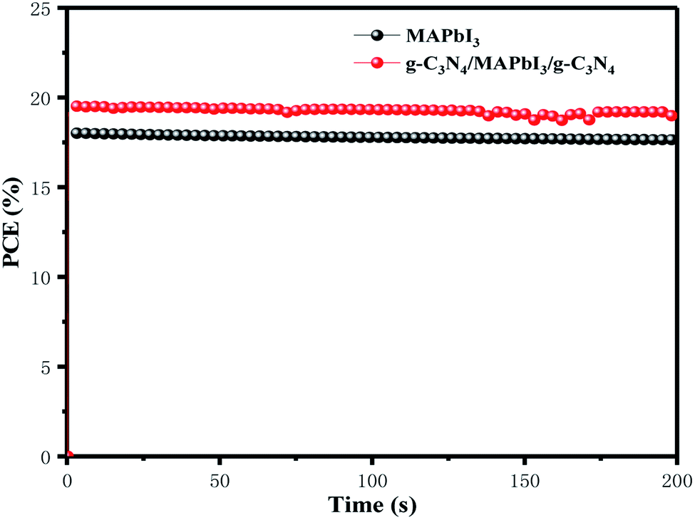 | ||
| Fig. 8 Steady-state efficiencies of PSCs with and without g-C3N4 dual-incorporation measured at maximum power output. | ||
4. Conclusions
We demonstrated a simple and effective method to fabricate n-type g-C3N4 ultrathin films at HTL/perovskite and ETL/perovskite interfaces in planar PSCs to obtain high efficiency and long-term stability. FF, Voc, and Jsc values were enhanced to 0.807, 1.14 V, and 21.45 mA cm−2, respectively, and enabled the PCE to increase to 19.67%. The better performance of the planar PSCs after g-C3N4 dual-incorporation was attributed mainly to two reasons: (i) g-C3N4 dual-incorporation enhanced the absorption of visible light by the perovskite layer; and (ii) the device with g-C3N4 dual-incorporation had a smaller Rs, smaller τave, and larger Rrec. This phenomenon helped to accelerate the charge extraction and transfer rates. Furthermore, ultrathin semiconductor films with Lewis base character may effectively passivate defects at the dual interfaces of the perovskite layer to achieve better PSC photovoltaic performance and long-term stability.Conflicts of interest
There are no conflicts to declare.Acknowledgements
This research was financially supported by the Key Program for Intergovernmental S&T Innovation Cooperation Projects of National Key R&D Program of China (2019YFE0107100), National Natural Science Foundation of China (5170021087), and China Postdoctoral Science.References
- Y. Wu, X. Li, S. Fu, L. Wan and J. Fang, J. Mater. Chem. A., 2019, 14, 8078–8084 RSC.
- G. C. Xing, N. Mathews, S. Y. Sun, S. S. Lim, Y. M. Lam, M. Gratzel, S. Mhaisalkar and T. C. Sum, Science, 2013, 6156, 344–347 CrossRef.
- S. D. Stranks, G. E. Eperon, G. Grancini, C. Menelaou, M. J. P. Alcocer, T. Leijtens, L. M. Herz, A. Petrozza and H. J. Snaith, Science, 2013, 6156, 341–344 CrossRef.
- M. Z. Liu, M. B. Johnston and H. J. Snaith, Nature, 2013, 7467, 395 CrossRef.
- M. Saliba, T. Matsui, K. Domanski, J. Y. Seo, A. Ummadisingu, S. M. Zakeeruddin, J. P. Correa-Baena, W. R. Tress, A. Abate, A. Hagfeldt and M. Gratzel, Science, 2016, 63, 206–209 CrossRef.
- Y. Li, L. Li, A. S. Yerramilli, Y. Chen, D. Fang, Y. Shen and T. L. Alford, Org. Electron., 2019, 73, 130–136 CrossRef CAS.
- X. Qi, G. Liu, D. Wang, N. Zhu, Y. Zhang, Z. Zhang, C. Wu, X. Li, W. Luo, Y. Li, H. Hu, Z. Chen, L. Xiao, S. Wang and B. Qu, Org. Electron., 2019, 74, 52–58 CrossRef CAS.
- H. Liu, Z. Chen, H. Wang, F. Ye, J. Ma, X. Zheng, P. Gui, L. Xiong, J. Wen and G. Fang, J. Mater. Chem. A, 2019, 17, 10636–10643 RSC.
- C. Chen, Z. Song, C. Xiao, D. Zhao, N. Shrestha, C. Li, G. Yang, F. Yao, X. Zheng, R. J. Ellingson, C.-S. Jiang, M. Al-Jassim, K. Zhu, G. Fang and Y. Yan, Nano Energy, 2019, 4, 141–147 CrossRef.
- G. Yang, H. Zhang, G. Li and G. Fang, Nano Energy, 2019, 63, 103835 CrossRef CAS.
- L. Wang, C. McCleese, A. Kovalsky, Y. Zhao and C. Burda, J. Am. Chem. Soc., 2014, 35, 12205–12213 CrossRef.
- C. Chen, Y. Jiang, J. Guo, X. Wu, W. Zhang, S. Wu, X. Gao, X. Hu, Q. Wang, G. Zhou, Y. Chen, J. M. Liu, K. Kempa and J. Gao, Adv. Energy Mater., 2019, 30, 1900557 Search PubMed.
- A. Klasen, P. Baumli, Q. Sheng, E. Johannes, S. A. Bretschneider, I. M. Hermes, V. W. Bergmann, C. Gort, A. Axt, H. Kim, H. J. Butt, W. Tremel and R. Berger, J. Phys. Chem. Lett., 2019, 22, 13458–13466 CrossRef.
- Z. Arain, C. Liu, Y. Yang, M. Mateen, Y. Ren, Y. Ding, X. Liu, Z. Ali, M. Kumar and S. Dai, Sci. China Mater., 2018, 2, 161–172 Search PubMed.
- B. Yang, C. C. Brown, J. Huang, L. Collins, X. Sang, R. R. Unocic, S. Jesse, S. V. Kalinin, A. Belianinov, J. Jakowski, D. B. Geohegan, B. G. Sumpter, K. Xiao and O. S. Ovchinnikova, Adv. Funct. Mater., 2017, 26, 1700749 CrossRef.
- F. Wang, M. Yang, S. Yang, X. Qu, L. Yang, L. Fan, J. Yang and F. Rosei, Nano Energy, 2019, 67, 104224 CrossRef.
- P. Schulz and D. Cahen, Chem. Rev., 2019, 5, 3349–3417 CrossRef.
- P. Wang, Q. Jiang, Y. Zhao, Y. Chen, Z. Chu, X. Zhang, Y. Zhou and J. You, Sci. Bull., 2018, 11, 726–731 CrossRef.
- Q. Jiang, Z. Chu, P. Wang, X. Yang, H. Liu, Y. Wang, Z. Yin, J. Wu, X. Zhang and J. You, Adv. Mater., 2017, 29, 1703852 CrossRef.
- J. Li, T. Bu, Y. Liu, J. Zhou, J. Shi, Z. Ku, Y. Peng, J. Zhong, Y.-B. Cheng and F. Huang, ChemSusChem, 2018, 17, 2898–2903 CrossRef.
- M. Wang, F. Cao, K. Deng and L. Li, Nano Energy, 2019, 63, 103867 CrossRef CAS.
- M. M. Tavakoli, M. Saliba and P. Yadav, Adv. Energy Mater., 2019, 4, 1900413 Search PubMed.
- Z. Liu, F. Cao, M. Wang, M. Wang and L. Li, Angew. Chem. Int. Ed., 2020, 10, 4161–4167 CrossRef.
- W. Ke, C. Xiao, C. Wang, B. Saparov, H. S. Duan, D. Zhao, Z. Xiao, P. Schulz, S. P. Harvey, W. Liao, W. Meng, Y. Yu, A. J. Cimaroli, C. S. Jiang, K. Zhu, M. Al-Jassim, G. Fang, D. B. Mitzi and Y. Yan, Adv. Mater., 2016, 26, 5214–5221 CrossRef.
- D. W. deQuilettes, K. Frohna, D. Emin, T. Kirchartz, V. Bulovic, D. S. Ginger and S. D. Stranks, Chem. Rev., 2019, 20, 11007–11019 CrossRef.
- W. Cao, K. Lin, J. Li, L. Qiu, Y. Dong, J. Wang, D. Xia, R. Fan and Y. Yang, J. Mater. Chem. C, 2019, 40, 12717–12724 RSC.
- F. Mohamadkhani, S. Javadpour and N. Taghavinia, Sol. Energy, 2019, 56, 647–653 CrossRef.
- H. Luo, J. Wu, X. Liu, Y. Yang, Q. Liu, M. Zhang, P. Yuan, W. Sun, Z. Lan and J. Lin, ACS Appl. Energy Mater., 2018, 12, 6700–6706 CrossRef.
- Z. Li, S. Wu, J. Zhang, Y. Yuan, Z. Wang and Z. Zhu, Sol RRL, 2019, 3, 1900413 Search PubMed.
- S. Wang, Y. Zhu, C. Wang and R. Ma, Small, 2019, 19, 11867–11876 Search PubMed.
- W. Hui, Y. Yang, Q. Xu, H. Gu, S. Feng, Z. Su, M. Zhang, J. Wang, X. Li, J. Fang, F. Xia, Y. Xia, Y. Chen, X. Gao and W. Huang, Adv. Mater., 2020, 4, 1906374 CrossRef.
- K. Wang, X. Liu, R. Huang, C. Wu, D. Yang, X. Hu, X. Jiang, J. C. Duchamp, H. Dorn and S. Priya, ACS Energy Lett, 2019, 8, 1852–1861 CrossRef.
- Q. Jiang, Y. Zhao, X. Zhang, X. Yang, Y. Chen, Z. Chu, Q. Ye, X. Li, Z. Yin and J. You, Nat. Photonics, 2019, 7, 460–466 CrossRef.
- J. Chen, H. Dong, L. Zhang, J. Li, F. Jia, B. Jiao, J. Xu, X. Hou, J. Liu and Z. Wu, J. Mater. Chem. A., 2020, 5, 2644–2653 RSC.
- S. S. Mali, J. V. Patil, H. Kim and C. K. Hong, Matter, 2019, 2, 452–464 CrossRef.
- B. Li, M. Li, C. Fei, G. Cao and J. Tian, J. Mater. Chem. A., 2017, 46, 24168–24177 RSC.
- L.-L. Jiang, Z.-K. Wang, M. Li, C.-C. Zhang, Q.-Q. Ye, K.-H. Hu, D.-Z. Lu, P.-F. Fang and L.-S. Liao, Am. J. Chem., 2018, 7, 1705875 Search PubMed.
- Y. Xiang, J. Yu, T. Zhang, Q. Wen, J. Zhuang and J. Guo, Mater. Sci. Semicond. Process., 2016, 15, 48–53 CrossRef.
- Z.-L. Yang, Z.-Y. Zhang, W.-L. Fan, C. Hu, L. Zhang and J.-J. Qi, Sol. Energy, 2019, 7, 859–865 CrossRef.
- A. B. Salyulev and A. M. Potapov, J. Phys. Chem. Lett., 2018, 3, 259–263 Search PubMed.
- P. Kumar, E. Vahidzadeh, U. K. Thakur, P. Kar, K. M. Alam, A. Goswami, N. Mahdi, K. Cui, G. M. Bernard, V. K. Michaelis and K. Shankar, J. Am. Chem. Soc., 2019, 13, 5415–5436 CrossRef.
- L. Zhao, Z. Zhao, Y. Li, X. Chu, Z. Li, Y. Qu, L. Bai and L. Jing, Nanoscale, 2020, 18, 10010–10018 RSC.
- K. Sun, J. Shen, Q. Liu, H. Tang, M. Zhang, S. Zulfiqar and C. Lei, Chin. J. Catal., 2020, 41, 72–81 CrossRef CAS.
- Y. Tian, L. Zhou, Q. Zhu, J. Lei, L. Wang, J. Zhang and Y. Liu, Nanoscale, 2019, 43, 20638–20647 RSC.
- H. Tang, R. Wang, C. Zhao, Z. Chen, X. Yang, D. Bukhvalov, Z. Lin and Q. Liu, Chem. Eng. J., 2019, 1064–1075 CrossRef CAS.
- W. Liu, J. Shen, X. Yang, Q. Liu and H. Tang, Appl. Surf. Sci., 2018, 369–378 CrossRef CAS.
- J. Dagar, S. Castro-Hermosa, G. Lucarelli, F. Cacialli and T. M. Brown, Nano Energy, 2018, 32, 290–299 CrossRef.
| This journal is © The Royal Society of Chemistry 2020 |