 Open Access Article
Electronic and optical properties of monolayer MoS2 under the influence of polyethyleneimine adsorption and pressure
Ong Kim Lea,
Viorel Chihaia b,
My-Phuong Pham-Ho*ac and
Do Ngoc Son
 *a
*a
aHo Chi Minh City University of Technology, VNU-HCM, 268 Ly Thuong Kiet Street, District 10, Ho Chi Minh City, Vietnam. E-mail: phmphuong@hcmut.edu.vn; dnson@hcmut.edu.vn
bInstitute of Physical Chemistry “Ilie Murgulescu” of the Romanian Academy, Splaiul Independentei 202, Sector 6, 060021 Bucharest, Romania
cInstitute for Computational Science and Technology, Quang Trung Software City, SBI Building, Street No. 3, Tan Chanh Hiep Ward, District 12, Ho Chi Minh City, Vietnam
First published on 27th January 2020
Abstract
MoS2 is one of the well-known transition metal dichalcogenides. The moderate bandgap of monolayer MoS2 is fascinating for the new generation of optoelectronic devices. Unfortunately, MoS2 is sensitive to gases in the environment causing its original electronic properties to be modified unexpectedly. This problem has been solved by coating MoS2 with polymers such as polyethyleneimine (PEI). Furthermore, the application of pressure is also an effective method to modify the physical properties of MoS2. However, the effects of polyethyleneimine and pressure on the electronic and optical properties of monolayer MoS2 remain unknown. Therefore, we elucidated this matter by using density functional theory calculations. The results showed that the adsorption of the PEI molecule significantly reduces the width of the direct bandgap of the monolayer MoS2 to 0.55 eV because of the occurrence of the new energy levels in the bandgap region due to the contribution of the N-2pz state of the PEI molecule. Remarkably, the transition from semiconductor to metal of the monolayer MoS2 and the MoS2/PEI system occurs at the tensile pressure of 24.95 and 21.79 GPa, respectively. The bandgap of these systems approaches 0 eV at the corresponding pressures. Importantly, new peaks in the optical spectrum of the clean MoS2 and MoS2/PEI appear in the ultraviolet region under compressive pressures and the infrared region under tensile strains.
1. Introduction
MoS2 is one of the most often studied transition metal dichalcogenides (TMDs)1–24 due to the convergence of many advanced properties for optical,1 electronic,2 and mechanical3 applications. Similar to graphene, the bonding between the layers of MoS2 is the weak van der Waals interaction. Therefore, the monolayer of MoS2 can be fabricated by exfoliation, which has a thickness of about 0.65 nm. In particular, the monolayer MoS2 has a direct bandgap of ca. 1.8 eV,4 which makes this material suitable for transistors,5 photodetectors, and light-emitting diodes.6 Field-effect transistors (FETs) of monolayer MoS2 demonstrated a high on/off current ratio exceeding 108 and the electron mobility of at least 200 cm2 V−1 s−1.5 The main problem of MoS2 is that it is sensitive to oxygen gas in air, which modifies its electronic properties unexpectedly. Thus, the bandgap becomes narrower and even disappeared after a few days of exposure to oxygen gas.7 To solve this problem, the dichalcogenide can be covered with polymers such as polyethyleneimine (PEI).8,9Furthermore, control of the electronic and optical properties of the monolayer MoS2 by changing the crystal structure,10 layer thickness,4 and applying strain11 was achieved. The results showed that the homogeneous biaxial tensile strain of around 10% led to the semiconductor-to-metal transition in all semiconducting TMDs.12 Several theoretical and experimental studies showed that the bandgap of the monolayer MoS2 decreases as the tensile strain increases,12,13 while it is a parabola for compression.14–17 Fan et al. demonstrated that the bandgap at the K point changes from direct to indirect with compressive pressure.14 Generally, the influence on the electronic structure properties of monolayer MoS2 depends on the type of applied strain. Experimentally, it is difficult to exert a homogeneous hydrostatic strain on a 2D material sample and can only generate a biaxial compressive strain up to 0.2% with elaborate setups.18 In a recent study, the monolayer MoS2 was investigated under extreme hydrostatic pressures of up to 30 GPa. Although a higher pressure is not experimentally achievable at present, a metallization at the compressive pressure of 68 GPa was predicted by theoretical calculations.19 In addition to the ability to tune the electronic properties of the monolayer MoS2, the applied strain was found to modify the photoluminescence (PL) intensity. The PL maximum peak of the monolayer MoS2 exhibited a blue shift20,21 at the rate of approximately 20 meV GPa−1. At the pressure of 25 GPa, both real and imaginary parts of the dielectric function were shifted to red, and the peak height increases correspondence with an enhancement of the optical absorption.21 These results demonstrated that one can adjust the electronic and optical properties of MoS2 by applying pressures. Interestingly, the monolayer MoS2 phototransistor exhibited a better photo-responsivity compared to the graphene-based devices.22
The effects of organic molecules adsorption such as TCNQ, TCNE, TTF, BV, F4TCNQ, and benzene on the electronic and optical properties of the monolayer MoS2 have been studied in the literature.23–26 A reduction of the bandgap was found due to the existence of the flat molecular levels of the organic molecules in the bandgap region of the monolayer MoS2. The theoretical study showed that the adsorption of TCNQ significantly enhances the peak height of the optical absorption of the monolayer MoS2 in the infrared region of the spectrum.23,24 Du et al. experimentally studied the adsorption of the PEI on multilayer MoS2 field-effect transistors.8 The experimental results demonstrated that a reduction of 2.6 times in sheet resistance and 1.2 times in contact resistance have been achieved. The enhancement of electrical properties was reflected in an improvement of 70% for ON-current and 50% for extrinsic field-effect mobility. Our previous study showed that the adsorption of the PEI molecule enhances the luminescence ability of the multi-layer MoS2 FET from 0.14 to 4.41 AW−1.9 However, the influences of both pressure and the PEI adsorption on the electronic and optical properties of MoS2 remain unknown. Therefore, in the present work, we are going to clarify this matter by using the density functional theory calculations.
1.1. Computational method
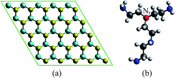
We used density functional theory calculations with the aid of the Vienna ab initio simulation package.27–29 The Perdew–Burke–Ernzerhof version of the generalized gradient approximation (GGA-PBE) was utilized for the exchange-correlation energy.30,31 The calculations of the band structure of monolayer MoS2 using various schemes have been summarized in the literature.32 The GGA functional plus van der Waals corrections underestimate the bandgap, while GW correction and HSE06 functional overestimate it. Local density approximation and GGA-PBE methods offered the most reasonable band gaps. Considering this result, as well as the accuracy in the geometries obtained by the GGA-PBE functional, in this study we used this functional to determine the effects of PEI doping on the MoS2 surface. The projector-augmented-wave method was taken into account for the electron–ion interactions.33,34 The plane-wave basis set was expanded with the cutoff energy of 600 eV. The surface Brillouin zone integration was performed by using the special k-point sampling technique of Monkhorst–Pack35 with the k-point mesh of 3 × 3 × 1. We also included the dipole corrections36,37 in the simulation for a periodic supercell to correct the interaction between the repeated images. The Gaussian smearing of order 0 with the sigma value of 0.1 was used to speed up the convergence of the calculations. The monolayer MoS2 (Fig. 1a) was modeled by the supercell approach using the 5 × 5 unit cell with the vacuum space of 16 Å along the z-direction. The vacuum space has been checked to make sure of no significant interaction of repeating images of the supercell. The truncated branched PEI fragment (Fig. 1b) was constructed based on the following requirements:9 (1) the total charge of the fragment is neutral, (2) the structure of the truncated fragment should contain nitrogen atoms accompany with one, two, and three alkyl groups. All atoms were allowed to fully relax during the geometry optimization until the Hellmann–Feynman force acting on each atom was less than 0.001 eV Å−1. Spin-polarized calculations were performed for the geometry optimization and the calculation of band structure.Adsorption energy was calculated to understand the binding strength of the PEI fragment on MoS2 through the formula:
| Ea = Esub+PEI − (Esub + EPEI), | (1) |
The pressure was estimated from the energy cost over the change of volume by:19
 | (2) |
 where a is the lattice constant and c is the thickness of the slab. We perform the modification of pressure by varying the lattice constant a while remaining the slab thickness.
Optical properties were determined through the frequency-dependent complex dielectric function, ε(ω) = ε1(ω) + iε2(ω)21,38 which is the measure of the light absorption and emission of material. The imaginary part of the dielectric constant ε2(ω) was computed by using the following expression:38
 | (3) |
 is the vector defining the polarization of the electric field of the incident light. The real part ε1(ω) can be calculated through ε2(ω) using the Kramer–Kronig relation,
 | (4) |
2. Results and discussion
2.1. The adsorption of the PEI fragment on the monolayer MoS2
We have to perform the geometric optimization of the monolayer MoS2 before the study of the PEI adsorption. The lattice constant of the monolayer MoS2 was optimized by the GGA-PBE method and obtained the parameters of a = b = 3.18 Å. The average bond length of Mo–S is 2.42 Å. The S–Mo–S and Mo–S–Mo angles are 82.30°. The thickness of the triple atomic layers of MoS2 is 3.13 Å. These results are in good agreement with the previous experimental and theoretical studies.23,39,40To study the influences of the pressure, we varied the lattice constant with the constraint a = b of the clean MoS2 and the MoS2/PEI system and explored the differences of two systems before and after changing the lattice constant. We considered the following values of the lattice constant: 2.84, 3.00, 3.18, 3.32, 3.48, and 3.64 Å. Two first values correspond to compressive strains and three last values correspond to the tensile strains.
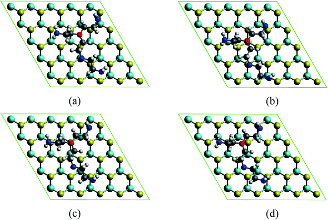
The MoS2/PEI system was prepared by loading the PEI fragment on the optimized monolayer MoS2. The MoS2/PEI system was allowed to fully relax for every step of the calculations. The PEI fragment was initially placed parallel to the surface of the monolayer MoS2 with a vertical distance of around 3.5 Å. Since the stability of the PEI adsorption correlates to the number of nitrogen atoms associated with the surface of the substrate, the stable geometry of the MoS2/PEI system was obtained with a flat structure of the PEI fragment on the surface of the monolayer MoS2. We considered several possible adsorption sites of the PEI molecule on the surface of MoS2, see Fig. 2. After performing the geometric optimization, we obtained the optimized structures of MoS2/PEI with the total energies of −741.39, −741.38, −741.43, and −741.41 eV for those in Fig. 2a–d, respectively. Based on these energies, we found the most favorable adsorption configuration of the PEI molecule as the N atom with three alkyl groups, denoted as Ny, positioned on the top of the S atom (Fig. 2c). The average vertical distance from the lowest nitrogen atoms, the lowest carbon atoms and the lowest hydrogen atoms of PEI to the surface of the substrate are 3.63, 3.76, and 2.37 Å, respectively.
We now perform the structural optimization for each variation of the lattice constant for the most favorable adsorption configuration of the PEI molecule on the MoS2 substrate. The adsorption energy of the PEI fragment on the substrate and the distances from this molecule to the substrate are listed in Table 1. We found that the distances increase slightly with the increase of the lattice constant.
| a (Å) | Ea (eV) | dN–S (Å) | dC–S (Å) | dH–S (Å) |
|---|---|---|---|---|
| 2.84 | 0.139 | 3.53 | 3.63 | 2.26 |
| 3.00 | 0.063 | 3.57 | 3.72 | 2.30 |
| 3.18 | −0.007 | 3.63 | 3.76 | 2.37 |
| 3.32 | −0.085 | 3.68 | 3.81 | 2.42 |
| 3.48 | −0.315 | 3.73 | 3.88 | 2.46 |
| 3.64 | −0.479 | 3.83 | 3.93 | 2.51 |
Furthermore, Fig. 3 shows that the adsorption energy becomes more negative; and hence, the favorable order of the PEI adsorption increases with the increase of the lattice constant. For the compression, with the lattice constant a < 3.18 Å, the adsorption energy is positive, which indicates that the adsorption of the PEI molecule is unstable on the surface of the monolayer MoS2. In contrast, for the cases of without strain (a = 3.18 Å) and tensile strains (a > 3.18 Å), the adsorption energy is negative. This result implies that the adsorption of the PEI molecule is stable. We found that the higher the lattice constant, the stronger the PEI molecule adsorbs. However, the interaction between the PEI molecule and the monolayer MoS2 is weak and the PEI molecule physisorbed on the MoS2. Furthermore, the phonon vibrational energy of the stretching mode of PEI is 0.43 eV. This value is comparable to the adsorption energy of PEI; therefore, the adsorption of PEI is thermodynamically unstable except for applying a high enough tensile pressure to the MoS2/PEI system.
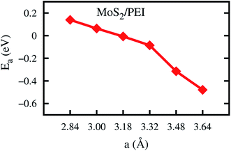 | ||
| Fig. 3 The adsorption energy of the PEI fragment on the monolayer MoS2 as a function of the lattice constant. | ||
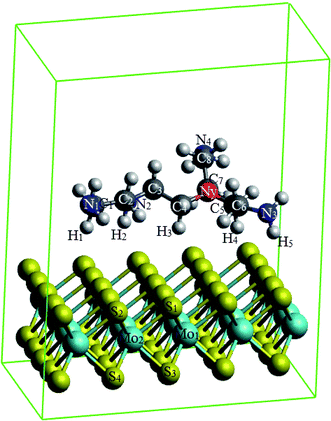
The structural information was shown in Table 2 for MoS2 and Table 3 for PEI with the change of lattice constant. We found that the average bond length between S1–S2, Mo–Mo, Mo–S, and the average bond angles Mo1–S1–Mo2, S1–Mo2–S2 increase, while the thickness of the MoS2 slab shown by S1–S3 and also the angle S1–Mo1–S3 decrease with the increase of lattice constant. Although the structural parameters for the MoS2 monolayer have been modified, the MoS2 monolayer under pressure remains the 2H phase similar to that of without strain. We can confirm this information by Fig. 4, where the top view of the MoS2 shows the honeycomb structure and the side views exhibit a similar structure for all considering lattice constants of 2.84, 3.18, and 3.64 Å. Table 3 shows the structural information of PEI that the bond lengths of N–C and C–C, and the bond angles of C–C–N and C–N–C somehow increase with the increase of the lattice constant.
| a (Å) | 2.84 | 3.00 | 3.18 | 3.32 | 3.48 | 3.64 | |
| Average bond length (Å) | S1–S2 | 2.85 | 3.06 | 3.18 | 3.32 | 3.48 | 3.57 |
| S1–S3 | 3.38 | 3.26 | 3.13 | 3.05 | 2.95 | 2.88 | |
| Mo1–Mo2 | 2.84 | 3.00 | 3.19 | 3.31 | 3.46 | 3.66 | |
| Mo–S | 2.37 | 2.38 | 2.41 | 2.45 | 2.49 | 2.53 | |
| Average bond angle (°) | Mo1–S1–Mo2 | 74.17 | 78.21 | 82.30 | 85.28 | 88.60 | 91.29 |
| S1–Mo2–S2 | 74.32 | 78.28 | 82.30 | 85.08 | 88.54 | 90.89 | |
| S1–Mo1–S3 | 91.66 | 87.65 | 80.54 | 79.42 | 73.07 | 70.98 | |
| a (Å) | 2.84 | 3.00 | 3.18 | 3.32 | 3.48 | 3.64 | |
| Bond length (Å) | Ny–C5 | 1.425 | 1.437 | 1.467 | 1.494 | 1.525 | 1.519 |
| Ny–C4 | 1.427 | 1.438 | 1.462 | 1.484 | 1.501 | 1.486 | |
| Ny–C7 | 1.443 | 1.451 | 1.471 | 1.488 | 1.498 | 1.483 | |
| N1–C1 | 1.457 | 1.459 | 1.465 | 1.494 | 1.468 | 1.455 | |
| N2–C2 | 1.450 | 1.444 | 1.461 | 1.472 | 1.486 | 1.474 | |
| N2–C3 | 1.436 | 1.451 | 1.463 | 1.478 | 1.488 | 1.469 | |
| N3–C6 | 1.459 | 1.461 | 1.464 | 1.470 | 1.469 | 1.459 | |
| N4–C8 | 1.458 | 1.460 | 1.463 | 1.466 | 1.461 | 1.448 | |
| C7–C8 | 1.509 | 1.519 | 1.543 | 1.570 | 1.615 | 1.635 | |
| C3–C4 | 1.512 | 1.524 | 1.538 | 1.556 | 1.591 | 1.599 | |
| C5–C6 | 1.508 | 1.514 | 1.537 | 1.558 | 1.588 | 1.578 | |
| Bond angle (°) | C6C5Ny | 111.32 | 113.10 | 116.54 | 119.13 | 122.96 | 123.74 |
| C4C3N2 | 110.41 | 112.37 | 115.27 | 117.23 | 118.62 | 118.63 | |
| C8C7Ny | 109.56 | 110.63 | 113.54 | 115.63 | 119.09 | 119.27 | |
| C3C4Ny | 109.81 | 111.11 | 115.02 | 117.74 | 121.79 | 122.44 | |
| C3N2C2 | 109.57 | 112.15 | 116.40 | 119.52 | 123.78 | 126.79 | |
| C5NyC4 | 113.45 | 113.52 | 114.45 | 115.11 | 116.75 | 116.77 | |
| C7NyC4 | 112.10 | 113.19 | 113.98 | 114.69 | 116.59 | 118.82 | |
| C7NyC5 | 111.90 | 110.93 | 111.71 | 112.22 | 113.97 | 111.86 | |
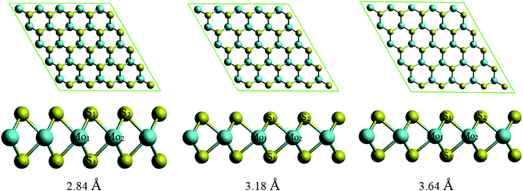 | ||
| Fig. 4 The upper and lower panels are the top and side views of the MoS2 slab with the change of lattice constant, respectively. | ||
2.2. Effects of the PEI adsorption and pressure on electronic structure properties of MoS2
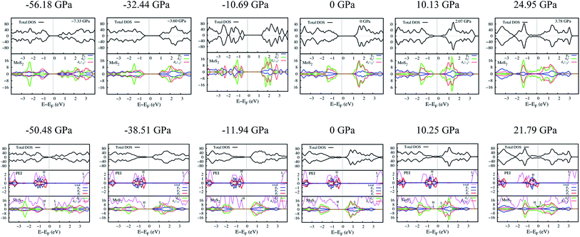
The effects of the PEI adsorption and the pressure variation by changing a = b on the electronic properties of the monolayer MoS2 were elucidated through the band structure, the density of states (DOS), and the charge exchange of the systems before and after these factors taking place.Fig. 6 shows that, at zero pressure, the monolayer MoS2 has a direct bandgap of 1.68 eV at the K point in the Brillouin zone, which is in good agreement with the previous publications.4,32,41 The total electronic density of states shows that the valence band maximum (VBM) and the conduction band minimum (CBM) are contributed mainly by Mo-4d states and weakly by S-3p states. The adsorption of the PEI molecule makes the energy levels of the MoS2/PEI system lower than that of the isolated monolayer MoS2, simultaneously creates new flat energy levels in the bandgap region which significantly decreases the direct bandgap of the monolayer MoS2 to 0.55 eV. The new energy levels appear in the region of the valence band of MoS2/PEI implying that the monolayer MoS2 became an n-type semiconductor upon the adsorption of the PEI molecule. The new flat energy levels mainly come from the contribution of the N-2p lone pair. Notably, at non-zero pressures, the bandgap of MoS2 and MoS2/PEI becomes narrower than that at zero pressure and gradually approaches 0 eV at some specific values of the pressure. When MoS2 and MoS2/PEI still show the semiconductor property, the significant difference between the electronic properties of two systems is that the bandgap of MoS2 changes from direct to indirect upon the variation of pressure, while MoS2/PEI remains direct bandgap with a smaller value due to the flat characteristics of the new energy levels but at a different position of the k-point mesh.
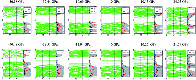 | ||
| Fig. 6 The band structure and total density of states of MoS2 (upper panel) and MoS2/PEI (lower panel) with the variation of pressure. | ||
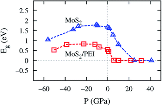
The pressure correspondence to the variation of the lattice constant of the MoS2 and MoS2/PEI systems was calculated by using the expression (2). The detailed values of the bandgap versus the pressure and the lattice constant were listed in Table 4. We found that the pressure varies from −56.18 to 41.14 GPa and −50.48 to 31.62 GPa for the lattice constant from 2.84 to 3.64 Å for the MoS2 and MoS2/PEI systems, respectively. The negative and positive signs represent the compressive and tensile strains in that order. We see that the pressure scale for the isolated MoS2 is similar to that for the MoS2/PEI system at the same value of the lattice constant.
| a (Å) | MoS2 | MoS2/PEI | ||
|---|---|---|---|---|
| P (GPa) | Eg (eV) | P (GPa) | Eg (eV) | |
| 2.84 | −56.18 | 1.05 | −50.48 | 0.53 |
| 3.00 | −32.44 | 1.55 | −38.51 | 0.81 |
| 3.04 | −27.65 | 1.72 | −22.44 | 0.83 |
| 3.12 | −10.69 | 1.80 | −11.94 | 0.82 |
| 3.16 | −9.46 | 1.75 | −8.12 | 0.69 |
| 3.18 | 0 | 1.68 | 0 | 0.55 |
| 3.20 | 1.53 | 1.61 | 0.95 | 0.46 |
| 3.24 | 5.04 | 1.29 | 5.74 | 0.02 |
| 3.32 | 10.13 | 0.81 | 10.25 | 0.01 |
| 3.48 | 24.95 | 0 | 21.79 | 0 |
| 3.64 | 41.14 | 0 | 31.62 | 0 |
The bandgap versus the pressure is visualized in Fig. 7. We found that the behavior of the bandgap for the isolated MoS2 is similar to that for MoS2/PEI, which is a parabola with a maximum value of 1.80 and 0.83 eV at the pressure of −10.69 and −22.44 GPa for the isolated MoS2 and MoS2/PEI systems, respectively. Furthermore, when the tensile pressure approaches 24.95 and 21.79 GPa, the bandgap approaches 0 eV for these systems in that order. This result implies that the monolayer MoS2 and MoS2/PEI systems transit from semiconductor to metal at the obtained values of the tensile pressure. The transition was found to be a little easier for the MoS2/PEI than the monolayer MoS2. The parabolic behavior of the bandgap is in good agreement with the experiment for the isolated MoS2.16
The amount of the charge exchange between the monolayer MoS2 and the PEI fragment was presented by the Bader point charge in Table 5. The plus and minus signs denote the charge gain and loss, respectively. Particularly, the hydrogen and carbon atoms donate while the nitrogen atoms gain charge. The total outcome is that the PEI molecule donates and the MoS2 gains charge. The charge exchange was found to inversely proportional to the bandgap. The higher the charge exchange, the narrower the bandgap becomes. This result supports the nature of the n-type doping to the substrate by the PEI polymer.
| P (GPa) | MoS2/PEI | Eg (eV) | F1 | F2 | F3 | F | ||||||
|---|---|---|---|---|---|---|---|---|---|---|---|---|
| 23H | 8C | 5N | 25Mo | 50S | PEI | MoS2 | ||||||
| −50.48 | −1.62 | −3.21 | 4.79 | −40.27 | 40.32 | −0.05 | 0.05 | 0.53 | −28.97 | −35.66 | 54.67 | −9.96 |
| −38.51 | −1.91 | −3.09 | 4.96 | −43.45 | 43.48 | −0.04 | 0.04 | 0.81 | −36.07 | −36.08 | 60.41 | −11.74 |
| 0 | −1.94 | −3.11 | 5.01 | −43.66 | 43.70 | −0.04 | 0.04 | 0.55 | −35.84 | −36.14 | 60.32 | −11.67 |
| 10.25 | −1.95 | −3.10 | 4.92 | −43.27 | 43.40 | −0.13 | 0.13 | 0.01 | −34.95 | −35.30 | 57.99 | −12.25 |
| 21.79 | −2.52 | −2.97 | 5.07 | −42.85 | 43.27 | −0.42 | 0.42 | 0 | −44.24 | −33.16 | 58.80 | −18.60 |
| 31.62 | −2.76 | −3.06 | 5.24 | −42.01 | 42.59 | −0.58 | 0.58 | 0 | −46.76 | −33.21 | 58.26 | −21.71 |
In common sense, a simple adsorbate will approach the substrate surface as its adsorption energy becomes more negative. However, for the complicated structure as the PEI molecule, as shown in Table 1, the distances from the nearest N, C, and H atoms of PEI to the surface of the MoS2 monolayer exhibit that the PEI molecule is slightly moving away from the surface as the lattice constant increases with the more negative adsorption energy. This observation seems to be contradicted; however, it can be explained in terms of the attractive electrostatic force between the PEI and the MoS2, which increases with the increase of the lattice constant. As shown in Table 5, the attractive force was found for the pairs of H–S and C–S and the repulsive force for the pairs of N–S atoms. The N–S repulsive force is strong enough to win the H–S and C–S attractive forces; and hence, it somehow lifts the whole PEI molecule away from the MoS2 surface. However, the total electrostatic force F remains the increasing attractive property with an increase in the pressure. The increasing attractive property of the total force is attributed mainly to the increase of the attractive interaction of the H atoms with the S atoms.
Fig. 8 presents the total DOS and the orbital projected DOS of the monolayer MoS2 and MoS2/PEI systems. At zero pressure, the total DOS exhibits a high symmetry of spin-up and spin-down components implying the non-magnetic properties of both MoS2 and MoS2/PEI systems. For the negative pressures, the projected DOS of the monolayer MoS2 shows that the contribution to the VBM and CBM is attributed to the dx2−y2 orbital of the Mo atoms and the px state of the S atoms. For the pressure ≥ 0, the dz2 orbital becomes dominant for the energy range near the Fermi level. The adsorption of the PEI molecule contributes to the occurrence of the new states, which comes from the contribution of the pz states of the N atoms. We can see more details in Fig. 9, the charge clouds of the Ny nitrogen atoms clearly exhibit the shape of the pz orbitals. The charge donation and accumulation distribute on the PEI fragment and the surface of the MoS2, respectively. This result is in good agreement with the behavior of the Bader point charge.
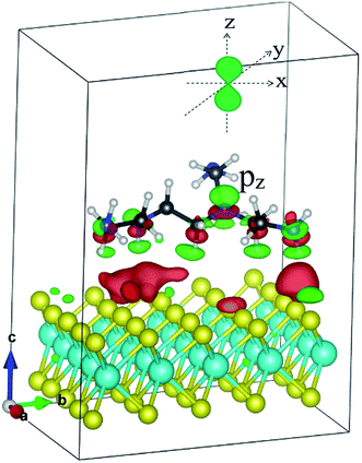 | ||
| Fig. 9 The charge density difference of the MoS2/PEI system. Occupied and unoccupied states are presented in red and green, respectively. | ||
The parabolic behavior of the bandgap, as shown in Fig. 7, is attributed to the different responses of the dx2−y2 and dz2 orbitals of the MoS2 monolayer toward the pressure, see Fig. 8 (upper panel). At the negative pressures, the dx2−y2 orbital plays the main role, while at the higher pressures, the dz2 orbital gradually becomes dominant at the VBM and CBM. The contribution from these orbitals is balanced at the VBM and CBM; and hence, the bandgap is broadest for the pressure of −10.69 GPa. When the dz2 orbital approaches the Fermi level, the bandgap becomes narrower, as the tensile pressure increases. Furthermore, the study of HOMO and LUMO can support the understanding of the interaction between the MoS2 substrate and the PEI adsorbate; and hence, the parabolic behavior of the MoS2/PEI bandgap. We presented the HOMO and LUMO states of the isolated MoS2 and isolated PEI in Fig. 8 (lower panel). The values of the MoS2 LUMO and the PEI HOMO were also listed in Table 6. We found that the HOMO–LUMO gap varies with the parabolic behavior as that of the bandgap of the MoS2/PEI system (Fig. 7), which increases first and then decreases with the increase of the pressure from the negative to the positive value.
| a (Å) | 2.84 | 3.00 | 3.12 | 3.16 | 3.18 | 3.32 | 3.48 | 3.64 | |
| Isolated PEI | HOMO (eV) | −0.51 | −0.53 | −0.49 | −0.53 | −0.56 | −0.51 | 0.00 | 0.00 |
| Isolated MoS2 | LUMO (eV) | 0.60 | 1.11 | 1.32 | 1.27 | 1.22 | 0.40 | 0.00 | 0.00 |
| LUMO–HOMO (eV) | 1.11 | 1.64 | 1.81 | 1.80 | 1.78 | 0.91 | 0.00 | 0.00 | |
2.3. Optical properties of MoS2 and MoS2/PEI
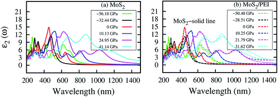
In this section, we studied the effects of the PEI adsorption and the pressure on the optical properties of the monolayer MoS2. The imaginary dielectric function ε2(ω) of MoS2 and MoS2/PEI systems were calculated through the expression (3) and shown in Table 7. The photon wavelength was calculated by using the formula λ = hc/Ep, where h is the Planck constant, c is the speed of light in vacuum, and Ep is the photon energy. The obtained result is listed in the third and seventh columns of Table 7.| P (GPa) | MoS2 | P (GPa) | MoS2/PEI | ||||||
|---|---|---|---|---|---|---|---|---|---|
| Eg (eV) | Ep (eV) | λ (nm) | ε2(ω) | Eg (eV) | Ep (eV) | λ (nm) | ε2(ω) | ||
| −56.18 | 1.05 | 4.66 | 266 | 11.06 | −50.48 | 0.53 | 4.61 | 269 | 9.98 |
| −32.44 | 1.55 | 2.60 | 477 | 11.58 | −38.51 | 0.81 | 2.76 | 449 | 11.10 |
| 0 | 1.68 | 2.73 | 453 | 14.88 | 0 | 0.55 | 2.72 | 456 | 14.91 |
| 10.13 | 0.81 | 2.39 | 521 | 13.36 | 10.25 | 0.01 | 2.35 | 527 | 13.38 |
| 24.95 | 0 | 2.00 | 621 | 13.18 | 21.79 | 0 | 2.01 | 618 | 12.86 |
| 41.14 | 0 | 1.42 | 873 | 12.06 | 31.62 | 0 | 1.41 | 877 | 11.12 |
As shown in Fig. 10a, at P = 0 GPa, the photoluminescence spectrum of the monolayer MoS2 exhibits the main peak at 453 nm within the range of visible light (400–800 nm). The result indicates that the MoS2 can absorb and emit the blue light, which is in agreement with the previous report.22,32 At non-zero pressures, the main PL peak shifts to the longer wavelength and simultaneously suppresses the peak height compared to that at zero pressure. Besides, for the positive pressure, the main peak tends to separate into two peaks. Furthermore, the intensity of the maximum PL is lower for the negative pressure than the positive pressure. We also found new peaks in the photoluminescence of the isolated MoS2 occurring in the ultraviolet region upon the compression and in the infrared region upon the tensile strain. The photoluminescence spectrum of the MoS2/PEI system in Fig. 10b remains almost unchanged compared to that of the isolated MoS2. This result implies that the benefit of the PEI coating is not only to protect the MoS2 from the adsorption of the unexpected gases but also remain the optical properties of the MoS2, which can be used for various optoelectronic applications.
3. Conclusion
In this paper, we have studied the electronic and optical properties of the monolayer MoS2 under the influences of the polyethyleneimine adsorption and the pressure. We found that the bandgap of the monolayer MoS2 reduces significantly upon the PEI adsorption, which was attributed to the pz state of the nitrogen atoms occurring in the bandgap region. The bandgap of MoS2 and MoS2/PEI systems approaches 0 eV at the tensile pressure of 24.95 and 21.79 GPa, respectively. The pressure also modifies the photoluminescence spectrum of the monolayer MoS2 and MoS2/PEI systems as shifting the main peak to the longer wavelength. Particularly, the compression and tensile strain generate new peaks in the ultraviolet and infrared regions, respectively. However, the PEI adsorption does not significantly alter the characteristics of the photoluminescence spectrum of the monolayer MoS2 at all pressure ranges. The coating of the polyethyleneimine does not only protect the monolayer MoS2 from the sensitive gases but also remain the optical properties of this system. This result is perhaps useful for the utilization of the MoS2/PEI in optoelectronic devices.Conflicts of interest
There are no conflicts of interest to declare.Acknowledgements
This research was funded by the Ho Chi Minh City Department of Science and Technology under contract number 310/QĐ-KHCNTT (2018). We acknowledge the usage of the computer time and software granted by the Institute of Physical Chemistry of Romanian Academy, Bucharest (HPC infrastructure developed under the projects Capacities 84 Cp/I of 15.09.2007 and INFRANANOCHEM 19/01.03.2009).References
- H. Zeng, J. Dai, W. Yao, D. Xiao and X. Cui, Valley polarization in MoS2 monolayers by optical pumping, Nat. Nanotechnol., 2012, 7(8), 490–493 CrossRef CAS PubMed.
- A. Enyashin and G. Seifert, Electronic properties of MoS2 monolayer and related structures, Nanosyst.: Phys., Chem., Math., 2014, 5(4), 517–539 Search PubMed.
- A. Castellanos-Gomez, M. Poot, G. A. Steele, H. S. J. van der Zant, N. Agraït and G. Rubio-Bollinger, Elastic properties of freely suspended MoS2 nanosheets, Adv. Mater., 2012, 24(6), 772–775 CrossRef CAS PubMed.
- K. F. Mak, C. Lee, J. Hone, J. Shan and T. F. Heinz, Atomically thin MoS2: a new direct-gap semiconductor, Phys. Rev. Lett., 2010, 105, 136805 CrossRef.
- B. Radisavljevic, A. Radenovic, J. Brivio, V. Giacometti and A. Kis, Single-layer MoS2 transistors, Nat. Nanotechnol., 2011, 6, 147–150 CrossRef CAS PubMed.
- Y. Yu, F. Miao, J. He and Z. Ni, Photodetecting and Light-Emitting Devices Based on Two Dimensional Materials, Chin. Phys. B, 2017, 26, 036801 CrossRef.
- J. Martincová, M. Otyepka and P. Lazar, Is Single Layer MoS2 Stable in the Air?, Chem.–Eur. J., 2017, 23, 13233–13239 CrossRef PubMed.
- Y. Du, H. Liu, A. T. Neal, M. Si and P. D. Ye, Molecular Doping of Multilayer MoS2 Field-Effect Transistors: Reduction in Sheet and Contact Resistances, IEEE Electron Device Lett., 2013, 0741–3106 Search PubMed.
- S. Hong, G. Yoo, D. H. Kim, W. G. Song, O. K. Le, Y. Ki Hong, K. Takahashi, I. Omkaram, D. N. Son and S. Kim, The doping mechanism and electrical performance of polyethylenimine-doped MoS2 transistor, Phys. Status Solidi C, 2017, 1600262 Search PubMed.
- M. Chhowalla, H. S. Shin, G. Eda, L.-J. Li, K. P. Loh and H. Zhang, The chemistry of two-dimensional layered transition metal dichalcogenide nanosheets, Nat. Chem., 2013, 5(4), 263–275 CrossRef PubMed.
- L. Yang, X. D. Cui, J. Zhang, K. Wang, M. Shen, S. Zeng, S. A. Dayeh, L. Feng and B. Xiang, Lattice strain effects on the optical properties of MoS2 nanosheets, Sci. Rep., 2014, 4, 5649 CrossRef CAS PubMed.
- P. Johari and V. B. Shenoy, Tuning the Electronic Properties of Semiconducting Transition Metal Dichalcogenides by Applying Mechanical Strains, ACS Nano, 2012, 6(6), 5449–5456 CrossRef CAS.
- Q. Yue, J. Kang, Z. Shao, X. Zhang, S. Chang, G. Wang, S. Qin and J. Li, Mechanical and electronic properties of monolayer MoS2 under elastic strain, Phys. Lett. A, 2012, 376, 1166–1170 CrossRef CAS.
- X. Fan, C.-H. Chang, W. T. Zheng, J.-L. Kuo and D. J. Singh, The Electronic Properties of Single-Layer and Multilayer MoS2 under High Pressure, J. Phys. Chem. C, 2015, 119, 10189–10196 CrossRef CAS.
- F. Li, Y. Yan, B. Han and T. Cui, Pressure confinement effect in MoS2 monolayers, Nanoscale, 2015, 7(19), 1–8 Search PubMed.
- M. López-Suárez, I. Neri and R. Rurali, Bandgap engineering of MoS2 upon compression, J. Appl. Phys., 2016, 119, 165105 CrossRef.
- X. Dou, K. Ding, D. Jiang and B. Sun, Tuning and Identification of Interband Transitions in Monolayer and Bilayer Molybdenum Disulfide Using Hydrostatic Pressure, ACS Nano, 2014, 8(7), 7458–7464 CrossRef CAS.
- Y. Y. Hui, X. Liu, W. Jie, N. Y. Chan, J. Hao, Y. T. Hsu, L. J. Li, W. Guo and S. P. Lau, Exceptional tunability of band energy in a compressively strained trilayer MoS2 sheet, ACS Nano, 2013, 7(8), 7126–7131 CrossRef CAS PubMed.
- A. P. Nayak, T. Pandey, D. Voiry, J. Liu, S. T. Moran, A. Sharma, C. Tan, C.-H. Chen, L.-J. Li, M. Chhowalla, J.-F. Lin, A. K. Singh and D. Akinwande, Pressure-Dependent Optical and Vibrational Properties of Monolayer Molybdenum Disulfide, Nano Lett., 2015, 15(1), 346–353 CrossRef CAS PubMed.
- X. Cheng, Y. Li, J. Shang, C. Hu, Y. Ren, M. Liu and Z. Qi, Thickness-dependent phase transition and optical behavior of MoS2 films under high pressure, Nano Res., 2018, 11, 855–863 CrossRef CAS.
- J. Shang, L. Zhang, X. Cheng and F. Zhai, Pressure induced effects on the electronic and optical properties of MoS2, Solid State Commun., 2015, 219, 33–38 CrossRef CAS.
- Z. Yin, H. Li, H. Li, L. Jiang, Y. Shi, Y. Sun, G. Lu, Q. Zhang, X. Chen and H. Zhang, Single-Layer MoS2 Phototransistors, ACS Nano, 2011, 6(1), 74–80 CrossRef PubMed.
- Y. Jing, X. Tan, Z. Zhou and P. Shen, Tuning electronic and optical properties of MoS2 monolayer via molecular charge transfer, J. Mater. Chem. A, 2014, 2, 16892–16897 RSC.
- S. Mouri, Y. Miyauchi and K. Matsuda, Tunable Photoluminescence of Monolayer MoS2 via Chemical Doping, Nano Lett., 2013, 13(12), 5944–5948 CrossRef CAS PubMed.
- Y. Wang, A. Slassi, M.-A. Stoeckel, S. Bertolazzi, J. Cornil, D. Beljonne and P. Samorì, Doping of Monolayer Transition-Metal Dichalcogenides via Physisorption of Aromatic Solvent Molecules, J. Phys. Chem. Lett., 2019, 10(3), 540–547 CrossRef PubMed.
- R. C. Selhorst, E. Puodziukynaite, J. A. Dewey, P. Wang, M. D. Barnes and A. R. T. Emrick, Tetrathiafulvalene-containing polymers for simultaneous non-covalent modification and electronic modulation of MoS2 nanomaterials, Chem. Sci., 2016, 7, 4698–4705 RSC.
- G. Kresse and J. Hafner, Ab initio molecular dynamics for open-shell transition metals, Phys. Rev. B: Condens. Matter Mater. Phys., 1993, 48, 13115–13118 CrossRef CAS PubMed.
- G. Kresse and J. Hafner, Ab initio molecular-dynamics simulation of the liquid-metal– amorphous-semiconductor transition in germanium, Phys. Rev. B: Condens. Matter Mater. Phys., 1994, 49, 14251–14269 CrossRef CAS PubMed.
- G. Kresse and J. Furthmuller, Efficient iterative schemes for ab initio total-energy calculations using a plane-wave basis set, Phys. Rev. B: Condens. Matter Mater. Phys., 1996, 54, 11169–11186 CrossRef CAS PubMed.
- J. P. Perdew, J. A. Chevary, S. H. Vosko, K. A. Jackson, M. R. Pederson, D. J. Singh and C. Fiolhais, Atoms, molecules, solids, and surfaces: applications of the generalized gradient approximation for exchange and correlation, Phys. Rev. B: Condens. Matter Mater. Phys., 1992, 46, 6671 CrossRef CAS PubMed.
- J. P. Perdew, K. Burke and M. Ernzerhof, Generalized Gradient Approximation Made Simple, Phys. Rev. Lett., 1996, 77, 3865 CrossRef CAS PubMed.
- Y. Li, Y.-L. Li, C. M. Araujo, W. Luo and R. Ahuja, Single-layer MoS2 as an efficient photocatalyst, Catal.: Sci. Technol., 2013, 3, 2214 RSC.
- P. E. Blochl, Projector augmented-wave method, Phys. Rev. B: Condens. Matter Mater. Phys., 1994, 50, 17953 CrossRef PubMed.
- G. Kresse and J. Joubert, From ultrasoft pseudopotentials to the projector augmented-wave method, Phys. Rev. B: Condens. Matter Mater. Phys., 1999, 59, 1758 CrossRef CAS.
- H. J. Monkhorst and J. D. Pack, Special points for Brillouin-zone integrations, Phys. Rev. B: Solid State, 1976, 13, 5188–5192 CrossRef.
- J. Neugebauer and M. Scheffler, Adsorbate-substrate and adsorbate-adsorbate interactions of Na and K adlayers on Al(111), Phys. Rev. B: Condens. Matter Mater. Phys., 1992, 46, 16067–16080 CrossRef CAS PubMed.
- L. Bengtsson, Dipole correction for surface supercell calculations, Phys. Rev. B: Condens. Matter Mater. Phys., 1999, 59, 12301–12304 CrossRef CAS.
- L. J. Kong, G. H. Liu and L. Qiang, Electronic and optical properties of O-doped monolayer MoS2, Comput. Mater. Sci., 2016, 111, 416–423 CrossRef CAS.
- N. Wakabayashi, H. G. Smith and R. M. Nicklow, Lattice dynamics of hexagonal MoS2 studied by neutron scattering, Phys. Rev. B: Solid State, 1975, 12, 659 CrossRef CAS.
- Y. Li, Z. Zhou, S. Zhang and Z. Chen, MoS2 Nanoribbons: High Stability and Unusual Electronic and Magnetic Properties, J. Am. Chem. Soc., 2008, 130, 16739–16744 CrossRef CAS PubMed.
- A. Splendiani, L. Sun, Y. Zhang, T. Li, J. Kim, C.-Y. Chim, G. Galli and F. Wang, Emerging Photoluminescence in Monolayer MoS2, Nano Lett., 2010, 10, 1271 CrossRef CAS PubMed.
| This journal is © The Royal Society of Chemistry 2020 |

