
 Open Access Article
 This Open Access Article is licensed under a Creative Commons Attribution-Non Commercial 3.0 Unported Licence
A Gd-doped HfO2 single film for a charge trapping memory device with a large memory window under a low voltage
Yuxin Shen†
 acd,
Zhaohao Zhang†be,
Qingzhu Zhangabd,
Feng Wei*a,
Huaxiang Yinbe,
Qianhui Weiac and
Kuo Menacd
acd,
Zhaohao Zhang†be,
Qingzhu Zhangabd,
Feng Wei*a,
Huaxiang Yinbe,
Qianhui Weiac and
Kuo Menacd
aState Key Laboratory of Advanced Materials for Smart Sensing, GRINM Group Co., Ltd., Beijing 100088, China. E-mail: weifeng@grinm.com
bKey Laboratory of Microelectronics Devices and Integrated Technology, Institute of Microelectronics, Chinese Academy of Sciences, Beijing 100029, China
cGRIMAT Engineering Institute Co., Ltd., Beijing 101402, China
dGeneral Research Institute for Nonferrous Metals, Beijing 100088, China
eUniversity of Chinese Academy of Sciences, Beijing 100049, China
First published on 24th February 2020
Abstract
In this study, a performance-enhanced charge trapping memory device with a Pt/Gd-doped HfO2/SiO2/Si structure has been investigated, where Gd-doped HfO2 acts as a charge trapping and blocking layer. The device demonstrates a large memory window of 5.4 V under a ±5 V sweeping voltage (360% of the device with pure HfO2), which is extremely attractive in low-power applications. In addition, the device also exhibits good retention characteristics with a 24.5% charge loss after the retention time of 1 × 10⁵ seconds and robust endurance performance with a 1% degradation after 1 × 10⁴ program/erase cycles. It is considered that the high density of defect states and the reduction in the defect energy levels induced by Gd-doping contribute to the performance improvement.
Introduction
Recently, charge-trapping memory (CTM) devices, such as a silicon-oxide-nitride-oxide-silicon (SONOS) structure flash memory, have attracted numerous interests for its potential for the further scale down below 15 nm node.1 Compared with the conventional floating-gate (FG) devices, CTM devices hold numerous advantages of higher reliability, lower operating voltage and simpler manufacturing process.1,2 However, there are still many challenges from the data retention due to the scaling of the thickness of tunnelling oxide and charge trapping oxide.3 To overcome these intrinsic shortcomings, high-k materials, such as HfO2, Al2O3, TiOx, ZnO and ZrO2, have been introduced into CTM devices to achieve better charge trapping efficiency and retention capability.4–10 Moreover, an ideal coexistence of a large memory window and low operating voltage is still a great challenge. Most present CTM devices have negligible memory window while operating at lower than 6 V. For high-k materials, doping is proved to be a potential approach to achieve low-power charging-trapping memories, such as Zr-doped BaTiO3 and fluorinated ZrO2.11,12 Gd-doped HfO2 (GHO), as one of promising high-k materials, has been proposed to have a relatively high trap density, large conduction band offset and high dielectric constant.13 Moreover, a GHO thin film also has excellent compatibility with CMOS processing. Therefore, it is expected that GHO should have good charge trapping characteristics and will be a promising candidate for the next generation flash memory. In recent years, the potential of GHO films for CTM applications has been proved,14 but the charge trapping mechanisms are still not well understood.In this study, Pt/GHO/SiO2/Si structure (MGOS) cells were fabricated and investigated for CTM applications, where the simple thin GHO film acts as the charge trapping and blocking layer. The experimental results demonstrate that the MGOS devices hold a remarkable charge-trapping efficiency. A large memory window of 5.4 V is observed under a low operating voltage of 5 V, while the P/E speed and retention characteristic are not sacrificed. Furthermore, the charge trapping mechanism of the MGOS is discussed.
Experiment
A 2-inch p-type (100) silicon wafer with a resistivity of 1–10 Ω cm was cleaned by the standard RCA process, and then the native oxide on the Si wafer was removed using diluted HF (DHF) solution for 3 min. Before the high-k deposition, a tunnelling oxide layer of 2 nm was thermally grown in the O3 atmosphere at 300 °C. Then, the GHO film was deposited via plasma-enhanced atomic layer deposition (PE-ALD) at 300 °C. During this process, Gd(TMHD)3, TDMAH, and O3 were used as the precursors for Gd, Hf, and O, respectively. In the following step, Pt top electrodes with an area of 3.8 × 10⁻⁴ cm2 were sputtered on the surface of the samples using a shadow mask at room temperature. Then, 300 nm Al was sputtered on the backside of the wafer as the bottom electrode. Finally, the samples were annealed at 300 °C for 5 min in argon atmosphere using a rapid thermal annealing (RTA) system. The electrical properties of the devices were characterized with a Keithley 4200 SCS analyzer. The cross-sectional morphology of the device was observed via high-resolution transmission electron microscopy (HRTEM). The defect states in the GHO films were investigated via photoluminescence (PL).Results and discussion
A schematic of the fabricated MGOS memory cells and the corresponding cross-sectional HRTEM image are shown in Fig. 1(a) and (b), respectively. As shown in Fig. 1(a), the thickness of the GHO layer is about 30 nm. Also, the SiO2 layer with bright contrast is about 2 nm in thickness, which indicates a uniform interface with Si to prevent charge tunnelling back to the Si substrate. The sharp interface between GHO and SiO2 is also observed, which means a less interdiffusion interface that can bring about a good device performance. In our experiments, the Gd concentration in the GHO thin film is 0.5% (determined via X-ray photoelectron spectroscopy), where the fabricated CTM devices present the optimum memory window.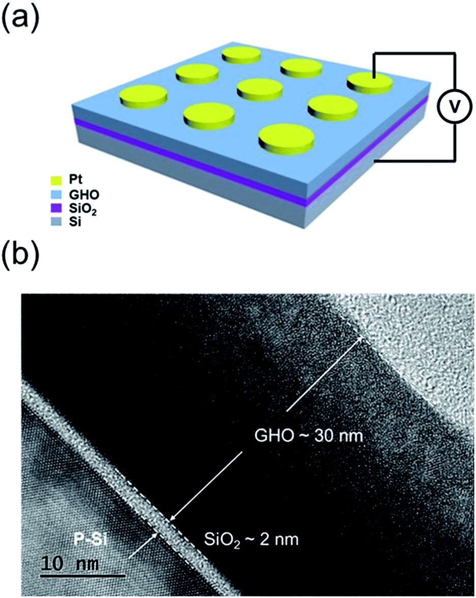 | ||
| Fig. 1 (a) A schematic of the MGOS device structure and (b) the cross-sectional HRTEM image for a single Gd-doped HfO2 film. | ||
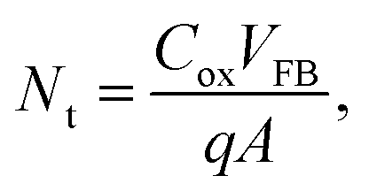
To study the memory properties of the MGOS devices, such as memory window, retention and endurance performance, the high frequency (1 MHz) capacitance–voltage (C–V) measurements were performed at room temperature. Fig. 2(a) demonstrates the C–V curves of the as-prepared devices under various sweeping gate voltages. The counterclockwise direction of the C–V hysteresis during a positive-negative-positive voltage sweep demonstrates the typical hysteresis loop direction of charge trapping. The memory window is defined as the difference in the flat-band voltages (VFB) between the program and erase states, which increases with the increase of the sweeping voltages. A large memory window of 5.4 V under a ±5 V sweeping voltage occurred, indicating an excellent charge trapping effect under a low operating voltage. When the sweeping voltage is further increased above 6 V, the memory window shows a saturation tendency and reaches the maximum value of 7.7 V under 10 V. The density of trapped charges per unit area (Nt) can be approximately estimated by the following equation:15
 | (1) |
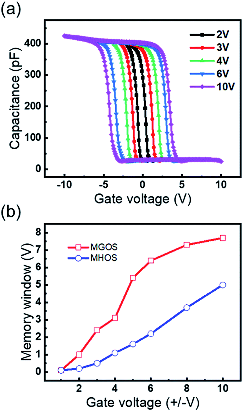 | ||
| Fig. 2 (a) High frequency (1 MHz) C–V characteristics of the MGOS device with GHO film; (b) memory window versus gate voltage characteristics of the MGOS and MHOS device. | ||
In the conventional tri-layer CTM devices, the quantum well is proposed to be responsible for the charge trapping effects, which usually formed by the different band offsets of the blocking layer, charge trapping layer and tunnelling layer.16,17 However, such a quantum well is not in this MGOS device as there is no blocking layer. Thus, the quantum well is not the origin of the excellent charge trapping effect. It has been reported that some intrinsic defects exist in the HfO2 films, such as oxygen vacancies and interstitial oxygen atoms, which induce defect energy levels.18 The high charge trapping efficiency is attributed to these defect energy levels.19 In this study, the charge trapping capability has a remarkable improvement as a result of the doping of Gd.
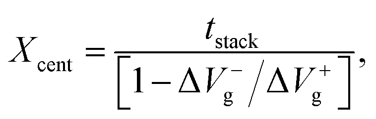
In order to prove the above viewpoint, the position of majority charge traps in this MGOS device was estimated with the calculation of charge trap centroid. The charge trap centroid (Xcent) can be calculated by the so-called constant current stress (CCS) method20 with the following equation:
 | (2) |
To further investigate the defect states of the GHO film, photoluminescence (PL) characterization was carried out. As shown in Fig. 3(a), the photoluminescence spectra under a 325 nm excitation wavelength shows clear PL peaks at 2.35–2.52 eV and 2.97–3.14 eV for the GHO film. Considering that the band gap of the GHO film is around 5.82 eV,13 we believe that the PL peaks at 2.35–2.52 eV and 2.97–3.14 eV cannot origin from the band-to-band recombination. Instead, it is most probably due to the recombination from defect states induced by VO to valence band (EV) or donor defect states to acceptor states, which indicates the existence of the high concentration defects in the GHO films.
 | ||
| Fig. 3 (a) Photoluminescence spectra of GHO films; (b) a schematic of the energy levels of the defect states and the programming process of the MGOS device; and (c) a schematic of the erasing process of the MGOS device. | ||
According to the theoretical simulations on defect energy levels, the defect states mainly occupy the donor levels rather than the acceptor levels in the GHO film.18 Therefore, the strongest PL peak at 2.43 eV shown in Fig. 3(a) is assigned to the recombination processes from the donor states at 2.43 eV above EV to the EV of the GHO film. It can be assumed that the electrons are first excited to the defect states of 2.43 eV above EV, and then recombine with the holes in the valence band with luminance. In conclusion, we put forward that the dominant defects are situated at 2.43 eV above the valence band. The energy level positions of the defect states are schematically shown in Fig. 3(b), where the band gaps of SiO2 and GHO are 9 eV and 5.82 eV, respectively. The charge trapping and escaping processes are schematically plotted in Fig. 3(b) and (c). Therefore, the efficient charge trapping processes in the MGOS device can be explained by the charge transfer between the defect states and the silicon substrate. It is ascertained that the dominant defect energy levels are located at 3.0 eV above the EV in pure HfO2 films.19 By contrast, the dominant defect energy levels in GHO films are located at 2.43 eV above EV. Therefore, we believe that the performance improvement under a low operating voltage can be ascribed to the energy level shift caused by Gd-doping.
The retention performance of the MGOS device was measured. As depicted in Fig. 4(a), the high and low capacitances are observed at a fixed read voltage of −1 V after ±5 V/1 s programming or erasing pulse voltage. After a 1 × 10⁵ s retention time, the capacitance of the device exhibits negligible degradation with only 1% charge loss, which is mainly caused by the direct tunnelling from the trap sites to the Si substrate at room temperature. The excellent retention capability can be attributed to the high potential barriers provided by defect states in the GHO film, which restrains the trapped charges from tunnelling back to the silicon substrate. To further investigate the retention properties, the flat band voltage (VFB) retention characteristics are also investigated, which are shown in Fig. 4(b). The VFB values retain the large value after 1 × 10⁵ s. The charge retention property of memory can be expressed as the percentage of trapped charge loss21 as below:
 | (3) |
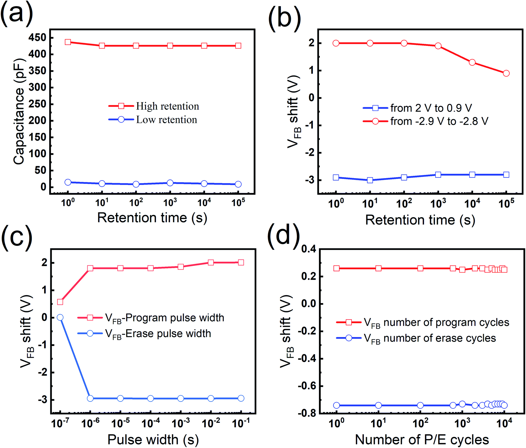 | ||
| Fig. 4 (a) The high and low capacitances of the memory device based on the single GHO layer and (b) the long-term retention characteristics of the VFB shift; (c) the program/erase characteristics of the MGOS device and (d) the endurance characteristic of the MGOS device at room temperature. | ||
To study the P/E characteristics of the MGOS device, voltage pulses of ±5 V with various duration are applied to the samples. As shown in Fig. 4(c), the speed of the P/E process is quite fast. With the increase in the pulse width, VFB increases rapidly in both program or erase operations. To reveal the endurance property, a P/E pulse voltage (±2 V with a pulse width of 10 ms) up to 104 cycles was applied to the MGOS device. As described in Fig. 4(d), both VFB curves show negligible degradation. After 104 cycles of the P/E operation, the VFB shifts are only 1% lower than their initial values. Therefore, this MGOS device demonstrates an admirable endurance performance, which is a necessary feature for future non-volatile memory devices.
Conclusion
In summary, we have investigated the memory characteristics and mechanism of the CTM device with the MGOS structure. A comparison of the memory windows at low operating voltages is summarized in Table 1 that includes the CTM devices with various structures. It is demonstrated that the device with a Pt/GHO/SiO2/Si structure holds great advantages in low-power consumption applications. A large memory window of 5.4 V is obtained under 5 V. Furthermore, the device also provides good retention characteristics, robust endurance performance, and fast program/erase speed. The efficient charge trapping effects under a low voltage can be attributed to the defect energy levels induced by the oxygen vacancies in the GHO films. Overall, the proposed MGOS structure is a promising candidate for future CTM applications.| Tunnelling layer | Charge trapping layer | Blocking layer | Operating voltage (V) | Memory window (V) | Total thickness (nm) | References |
|---|---|---|---|---|---|---|
| SiO2 | Gd:HfO2 | Gd:HfO2 | ±5 | 5.4 | 32 | This work |
| Al2O3 | HfO2 | Al2O3 | ±6 | 0.8 | 28 | 2 |
| SiO2 | Zr0.5Hf0.5O2 | Zr0.5Hf0.5O2 | ±5 | 2.0 | 52.5 | 6 |
| SiO2 | Ba0.6Sr0.4TiO3 | Ba0.6Sr0.4TiO3 | ±7 | 1.1 | 27 | 10 |
| SiO2 | NiO | SiO2 | ±5 | 2.1 | 33 | 17 |
| SiO2 | HfO2 | HfO2 | ±6 | 2.4 | 59 | 19 |
| Al2O3 | HfAlO | Al2O3 | ±6 | 4.1 | 23 | 22 |
| Al2O3 | ZnO/graphene/ZnO | Al2O3 | ±6 | 4.0 | 22.6 | 23 |
Conflicts of interest
The authors declared that they have no conflicts of interest to this work.Acknowledgements
This work was supported in part by National Natural Science Foundation of China under grants (61904194), in part by the youth foundation of General Research Institute for Nonferrous Metals under grant (66271903), in part by Youth Innovation Promotion Association, Chinese Academy of Sciences under grant (Y9YQ01R004).References
- P. Y. Du, H. T. Lue, Y. H. Shih, and K. Y. Hsieh, in IEEE International Conference on Solid-State and Integrated Circuit Technology, 2015, pp. 1–4 Search PubMed.
- X. Lan, X. Ou, Y. Cao, S. Tang, C. Gong, B. Xu, Y. Xia, J. Yin, A. Li and F. Yan, J. Appl. Phys., 2013, 114(4), 044104 CrossRef.
- H. W. You and W. J. Cho, Appl. Phys. Lett., 2010, 96, 093506 CrossRef.
- K. Jiang, X. Ou, Z. Y. Cao, X. J. Liu, W. Lu, B. Xu, A. D. Li, Y. D. Xia and Z. G. Liu, Appl. Phys. Lett., 2014, 104(26), 263506 CrossRef.
- G. H. Park and W. J. Cho, Appl. Phys. Lett., 2010, 96, 043503 CrossRef.
- J. H. Zhao, X. B. Yan, Y. C. Li, T. Yang, X. L. Jia, Z. Y. Zhou and Y. Y. Zhang, J. Appl. Phys., 2016, 120(14), 145304 CrossRef.
- P. Ding, Y. B. Yang, Y. R. Wang, C. Liu, J. Yin, Y. D. Xia, A. D. Li and Z. G. Liu, Appl. Phys. Lett., 2019, 114, 053506 CrossRef.
- Z. G. Xu, C. X. Zhu, Z. L. Huo, S. J. Zhao and M. Liu, J. Phys. D: Appl. Phys., 2012, 45, 185103 CrossRef.
- E. Hourdakis and A. G. Nassiopoulou, Microelectron. Eng., 2011, 88, 1573 CrossRef CAS.
- Y. Y. Zhang, T. Yang, X. B. Yan, Z. C. Zhang, G. Bai, C. Lu, X. L. Jia, B. F. Ding, J. H. Zhao and Z. Y. Zhou, Appl. Phys. Lett., 2017, 110, 223501 CrossRef.
- X. D. Huang, J. K. O. Sin and P. T. Lai, IEEE Electron Device Lett., 2013, 34(4), 499–501 CAS.
- X. D. Huang, R. P. Shi and P. T. Lai, Appl. Phys. Lett., 2014, 104(16), 162905 CrossRef.
- Y. H. Xiong, H. L. Tu, J. Du, M. Ji, X. Q. Zhang and L. Wang, Appl. Phys. Lett., 2010, 97, 012901 CrossRef.
- J. C. Wang, P. C. Chou, C. S. Lai and L. C. Liu, J. Vac. Sci. Technol., B: Nanotechnol. Microelectron.: Mater., Process., Meas., Phenom., 2011, 29, 011009 Search PubMed.
- X. B. Yan, T. Yang, X. L. Jia, J. H. Zhao and Z. Y. Zhou, Phys. Lett. A, 2017, 380(42), 3509 CrossRef.
- W. J. Lu, Y. H. Dai, F. F. Wang, F. Yang, C. Z. Ma, X. Zhang and X. W. Jiang, AIP Adv., 2017, 125001 CrossRef.
- N. Nakagawa, H. Y. Hwang and D. A. Muller, Nat. Mater., 2006, 5, 204 CrossRef CAS.
- K. Xiong, J. Robertson, M. C. Gibson and S. J. Clark, Appl. Phys. Lett., 2005, 87(18), 183505 CrossRef.
- Y. Zhang, Y. Y. Shao, X. B. Lu, M. Zeng, Z. Zhang, X. S. Gao, X. J. Zhang, J. M. Liu and J. Y. Dai, Appl. Phys. Lett., 2014, 105(17), 172902 CrossRef.
- X. D. Huang, L. Liu, J. P. Xu and P. T. Lai, Appl. Phys. Lett., 2011, 99(11), 112903 CrossRef.
- J. C. Wang, C. S. Lai, Y. K. Chen, C. T. Lin, C. P. Liu, M. R. S. Huang and Y. C. Fang, Electrochem. Solid-State Lett., 2009, 12(6), H202 CrossRef CAS.
- X. Lan, C. Gong, X. Ou, Y. Cao, C. Sun, Y. Chen, B. Xu, Y. Xia, A. Li and J. Yin, Microelectron. Eng., 2015, 133, 88 CrossRef CAS.
- N. El-Atab, F. Cimen, S. Alkis, A. K. Okyay, A. Nayfeh and A. Nayfeh, Appl. Phys. Lett., 2014, 105(3), 033102 CrossRef.
Footnote |
| † These authors contributed equally to the work. |
| This journal is © The Royal Society of Chemistry 2020 |