
 Open Access Article
 This Open Access Article is licensed under a Creative Commons Attribution-Non Commercial 3.0 Unported Licence
Theoretical study of a p–n homojunction SiGe field-effect transistor via covalent functionalization†
Jianwei Zhaoa,
Na Cheng a,
FeiFei Xiab,
LianMei Liua and
Yuanyuan He*a
a,
FeiFei Xiab,
LianMei Liua and
Yuanyuan He*a
aCollege of Material and Textile Engineering, Jiaxing University, Jiaxing 314001, Zhejiang, P. R. China. E-mail: heyy@mail.zjxu.edu.cn
bSchool of Chemical and Environmental Engineering, Jiangsu University of Technology, Changzhou 213001, Jiangsu, P. R. China
First published on 21st February 2020
Abstract
p–n homojunctions are superior to p–n heterojunctions in constructing nanoscale functional devices, owing to the excellent crystallographic alignment. We tune the electronic properties of monolayer siligene (SiGe) into p/n-type via the covalent functionalization of electrophilic/nucleophilic dopants, using ab initio quantum transport calculations. It is found that the n-type doping effect of K atoms is stronger than that of benzyl viologen (BV) molecule on the surface of SiGe monolayer, owing to the strong covalent interaction. Both of p-type 2,3,5,6-tetrafluoro-7,7,8,8-tetracyanoquinodimethane (F4TCNQ)-adsorbed and n-type 4 K-adsorbed SiGe systems show enhanced optical absorption in the infrared region, indicating their promising applications in infrared optoelectronic devices. By spatially adsorbing F4TCNQ molecule and K atoms on the source and drain leads, respectively, we designed a p–n homojunction SiGe field-effect transistor (FET). It is predicted that the built F4TCNQ-4K/SiGe FET can meet the requirements for high-performance (the high current density) and low-power (low subthreshold swing (SS)) applications, according to the International Technology Roadmap for Semiconductors in 2028. The present study gains some key insights into the importance of surface functionalization in constructing p–n homojunction electronic and optoelectronic devices based on monolayer SiGe.
1. Introduction
Semiconductor p–n junctions are the fundamental building blocks for electronic and optoelectronic devices.1–3 Up to now, p–n heterojunction and homojunction architectures have been widely applied in modern electronics.4–6 A p–n heterojunction is formed by joining two different semiconductors, which can take advantage of the large variety of electronic properties available among different semiconductors to efficiently separate charge.7,8 However, the large interfacial-trap density and uneven interfacial roughness degrades its device performance under optimal working condition.9,10 In comparison, p–n homojunction has been intensively explored as a new emerging configuration, which is based on a single semiconductor. p–n homojunctions normally possess superior electronic and optoelectronic properties, because the excellent crystallographic alignment can eliminate the lattice mismatch and thus endow the material with perfect band alignment.11–13 For instance, n-type O-defective TiO2 quantum dot-decorated p-type Ti-defective TiO2 exhibits excellent performance in photoelectrochemical and photocatalytic hydrogen generation, holding great promise toward the application of p–n homojunctions in highly-efficient photocathodes for hydrogen generation.14The development of two-dimensional (2D) semiconductors offers additional flexibility and functionality to the design of p–n homojunction architectures, owing to their ultra-thin thickness as well as novel electronic and optical properties.15–17 The performance of 2D p–n homojunction nanodevices relies on controllable doping of 2D semiconductors. The conventional doping method takes effect by incorporating dopants into the host semiconductor lattices, but the damage in lattice structure as well as limited dopant solubility restricts the application of this method in 2D semiconductors. Alternatively, surface functionalization is a simple, nondestructive, and effective strategy to construct 2D p–n homojunctions, in which a specific region is p-/n-doped by the adsorption of electrophilic/nucleophilic molecules, nanoparticles, or quantum dots. Jing, et al. disclosed that 2,3,5,6-tetrafluoro-7,7,8,8-tetracyanoquinodimethane (F4TCNQ) and benzyl viologen (BV) could enhance the optical properties of MoS2 and phosphorene for effective light harvesting.18,19 Surface-functionalized p–n homojunction has been proven superior to those formed by the other methods, such as thickness-based, electrostatical-doped, or elemental-doped p–n homojunctions,14,20,21 because the great variety of surface dopants offers convenience to modulate the device performance based on 2D p–n homojunctions in a wide range. Experimentally, 2D p–n homojunction based on transition metal dichalcogenide family, including WS2, MoTe2, ReS2, and so on, have been realized by surface functionalization strategy and applied in high-performance electronic and optoelectronic nanodevices.22–24 For instance, McKone et al. built WSe2 p–n homojunction by depositing noble metals on p-type WSe2, whose photoelectrode energy-conversion efficiency can be higher than 7% for the hydrogen evolution reaction.25 In spite of the great progress, the poor compatibility with current Si-based technology has severely hindered the above 2D semiconductors in the mass application of p–n homojunction devices. To solve this problem, monolayer siligene (SiGe) as a new 2D atomic semiconductor has stimulated extensive research interests, not only due to the preserved Dirac cones, but also because of the improved stability in comparison with pristine silicene and germanene.26,27 In 2003, Hu et al. successfully synthesized atomic-thick SiGe films, via chemical vapor deposition of precursors containing precise atomic arrangements with Si–Ge bonds.28 However, monolayer SiGe-based p–n homojunction nanodevices have not been realized in practice hitherto, since the spatial doping strategy on the surface of SiGe monolayer requires to be explored. Thus, it is necessary to develop a feasible method to rationally dope electrons/holes into monolayer SiGe, which will facilitate the construction of p–n homojunction based on monolayer SiGe.
Herein, based on ab initio quantum-transport simulations, we investigate the effect of surface functionalization on the electronic and optoelectronic properties of monolayer SiGe, by means of the adsorption of electrophilic/nucleophilic dopants, including F4TCNQ, BV molecules, and K atoms. It is found that electrophilic F4TCNQ molecule can withdraw electrons from SiGe monolayer, whereas nucleophilic K atoms can inject electrons into SiGe monolayer, in virtue of the strong charge transfer between the surface dopants and SiGe substrate. p–n homojunction field-effect transistor (FET) based on monolayer SiGe is constructed by adsorbing F4TCNQ molecule and 4 K atoms on the source and drain leads, respectively. The excellent current density and subthreshold swing (SS) value demonstrate that the designed F4TCNQ-4K/SiGe can meet the demand for high-performance and low-power devices in International Technology Roadmap for Semiconductors (ITRS) of 2028. These fundamental findings suggest that SiGe, as a novel 2D material, is of great potential in the future Si-based p–n homojunction electronic and optoelectronic nanodevices, via surface functionalization.
2. Computational methods
The geometric optimization and electronic calculation were carried out by employing the linear combination of atomic orbitals (LCAO) technique, with the assistance of Atomistix-tool-kit Virtual-nano-lab (ATK-VNL) package.29–31 The generalized gradient approximation (GGA) expressed by Perdew–Burke–Ernzerhof (PBE) functional was used in all calculation.32 The core and valence electron partitions were defined by SG15 optimized non-conserving Vanderbilt (ONCV) pseudopotentials, to avoid underestimating the bandgap.33 To consider the van der Waals (vdW) interaction, specialized Grimme's approach (DFT-D3) was adopted to correct the dispersion between SiGe monolayer and the adsorbed p-/n-type dopants.34 The kinetic-energy cut-off was set as 100 Hartree. A regular 8 × 1 × 8 unshifted Monkhorst–Pack grid of k-points was sampled in the Brillouin zone during geometric optimization.35 A vacuum slab of 25 Å was selected to avoid the mirror interaction between adjacent layers. The structures of SiGe monolayers before and after surface functionalization were fully relaxed until the force and stress were less than 1.0 × 10⁻⁴ eV Å−1 and 5.0 × 10⁻⁴ GPa, respectively. Much denser k-point meshes (12 × 1 × 12) were used to obtain the accurate band structure and density of states (DOS). The DFT-1/2 method was employed for quasiparticle correction, which has been widely applied to predict the bandgap of 2D semiconductors.36Subsequently, the electronic transport behavior of SiGe monolayer before and after surface functionalization was investigated by combining ab initio and quantum transport calculations in ATK-VNL.37 A two-probe model of the bottom-gated SiGe FET was constructed with pristine monolayer SiGe as the electrodes and surface-functionalized SiGe as the channel, on which p-/n-type dopants were adsorbed. In the central region, the positions of adsorbed dopants were further optimized until the force was less than 0.10 eV Å−1. The scattering region in the 2 × 1 × 1 supercell of SiGe was long enough to screen the charge oscillation on the contacts between electrodes and channel region.38 The k-point meshes for the channel region and source/drain electrodes were sampled with 2 × 1 × 1 and 2 × 1 × 150, respectively. The entire studied systems were purely ballistic and the phonon scattering will not be considered. According to the Landauer–Büttiker formula, the source-drain current (IDS) was calculated as follows:39
 | (1) |
3. Results and discussion
SiGe monolayer is a novel kind of two-dimensional semiconductor with graphene-like planner structure, in which the incorporation of Si and Ge atoms can not only preserve the Dirac cones, but also improve the dynamic stability, relative to the pristine silicene and germanene.27,43 To controllably dope electrons/holes into monolayer SiGe, we first modeled pristine SiGe and surface-functionalized SiGe monolayers with different adsorbed dopants based on first-principle method. As shown in Fig. 1a–c, F4TCNQ molecule is a typical p-type dopant, which is usually physisorbed on the surface of 2D materials, whereas BV molecule and K atoms are typical n-type dopants.19,44–46 Similarly, BV molecule is also physisorbed on the surface of 2D materials. In this work, 4 K atoms are regarded as a whole and expected to be chemically anchored on monolayer SiGe. In addition, the distances between adjacent K atoms are set 7.87 and 13.54 Å, which are long enough to eliminate any interaction between adjacent K atoms. Fig. 1d–g present the fully relaxed structures of 4 × 4 SiGe monolayer before and after the surface functionalization of all above dopants. The vertical distances between F4TCNQ, BV molecules, K atoms and SiGe monolayer are ∼2.00, ∼2.82, and ∼2.48 Å, respectively. The corresponding adsorption energies (ΔE) are −3.52, −0.42, and −6.39 eV, which are defined as follows:| ΔE = Edopant/SiGe − Edopant − ESiGe, | (2) |
 | ||
| Fig. 1 Top views of optimized structures of (a) F4TCNQ molecule as p-type dopant, (b) BV molecule and (c) 4 K atoms as n-type dopants. (d–g) Top and side views of the fully relaxed structure models of SiGe monolayer with F4TCNQ, BV, and 4 K adsorption, respectively. | ||
To quantitatively verify the interaction between different surface dopants and SiGe monolayer, the charge transfer amounts in the surface functionalized SiGe systems were calculated in terms of Mulliken population analysis with DFT-1/2 method in Table 1. It is remarkably observed that F4TCNQ can accept about 1.79 electrons from monolayer SiGe, revealing that F4TCNQ can act as a strong acceptor on the surface of monolayer SiGe. This is largely attributed to that the existence of fluorine and cyano groups endows F4TCNQ molecule with strong electrophilic properties. In contrast, as a strong nucleophilic dopant, the adsorption of K atoms has led 3.14 electrons transferred into SiGe substrate, which is much larger than that (0.54 electrons) in BV/SiGe system. The reason for this phenomenon is that ionic K–Si bond as a kind of chemisorption is much stronger than the physisorption of BV molecule on SiGe substrate. In addition, the metallic property of K atoms also contributes to its strong nucleophilic properties, which can be applied to inject electrons into SiGe monolayer. The charge transfer in surface functionalized SiGe systems can also be visualized in charge density differences (Δρ) as shown in Fig. 2. The region of electron gain/loss is displayed in blue/red color. Δρ is defined as Δρ = ρdopant/SiGe − ρSiGe − ρdopant, in which ρdopant/SiGe, and ρSiGe are the charge densities of the dopant-adsorbed SiGe system with and without surface functionalization with dopants, ρdopant is the charge density of the isolated dopant molecule/atoms, respectively. It is worth noting that the adsorption of surface dopant has brought about remarkable charge redistribution on the interface between dopants and SiGe monolayer. A large number of electrons are withdrawn from monolayer SiGe to physisorbed F4TCNQ molecule, revealing that F4TCNQ can act as acceptor to inject holes into SiGe. On the contrary, the chemisorption of 4 K atoms will donate electrons into SiGe substrate. The electron depletion around BV molecule has been weakened by the physisorption of BV molecule on SiGe monolayer, in comparison of the strong chemisorption of K atoms. Thereupon, holes/electrons can be effectively doped into monolayer SiGe (i.e. monolayer SiGe can be p-/n-type doped), via surface functionalization with F4TCNQ molecule and 4 K atoms, respectively.
 | ||
| Fig. 2 DFT-1/2 charge density differences (e/Å3) of (a) F4TCNQ/SiGe, (b) BV/SiGe, and (c) 4K/SiGe systems. Blue and red colors represent electron accumulation and depletion, respectively. | ||
The interaction between surface dopants and monolayer SiGe can also affect the electronic properties of monolayer SiGe. The left panels in Fig. 3 give the band structures of monolayer SiGe before and after surface functionalization. Obviously, surface functionalization narrows the bandgap with different degrees, compared with that of pristine SiGe monolayer (0.51 eV), owing to the introduced energy levels in the gap region.47 In p-type doped F4TCNQ/SiGe system, the bandgap energy is reduced to 0 eV, which is attributed to the strong orbital hybridization between F4TCNQ and SiGe substrate in the valence region.48 The new energy levels above the Fermi level are generated by the adsorption of F4TCNQ molecule, as indicated by the projected densities of states (PDOS) in the right panel of Fig. 3a. It is deduced that the work function of monolayer SiGe can be effectively increased, since the original Fermi level (EF) in pristine SiGe is downshifted remarkably by the new-generated empty bands in the conduction region. Analogously, the reduced bandgap (0 eV) in n-type doped 4K/SiGe system is caused by the strong orbital hybridization between 4 K atoms and SiGe substrate in the conduction region. Meanwhile, the work function can be decreased by the upshifted EF in 4K/SiGe system. Hence, the strong orbital hybridization between F4TCNQ molecule/4 K atoms and underlying SiGe monolayer results in the shallow acceptor/donor states for p-/n-type doping. As for BV/SiGe system, the conduction band minimum (CBM) is slightly closer to EF than VBM, indicating its weak n-type semiconductive property. The reason for this phenomenon is that the electron-donating capability of BV molecule is weaker than K atom. In light of the band structure as well as DOS spectra, it can be concluded that F4TCNQ molecule can tune the electronic properties of monolayer SiGe into p-type, whereas 4 K atoms can tune it into n-type, whose n-type doping effect is much stronger than BV molecule, via surface functionalization.
 | ||
| Fig. 3 Calculated DFT-1/2 electronic band structures (left panels), total DOS and PDOS (right panels) of (a) pristine SiGe, (b) F4TCNQ/SiGe, (c) BV/SiGe, and (d) 4K/SiGe monolayers, respectively. The Fermi level is indicated by the red dashed line. | ||
The change of interaction between surface dopants and SiGe monolayer can also influence the optical properties of monolayer SiGe. Fig. 4 presents the optical absorption spectra of monolayer SiGe systems before and after surface functionalization. Generally speaking, a direct bandgap can ensure the production of photocurrent.49 A sharp absorption peak emerges in the visual region for pristine SiGe monolayer, suggesting that light within a wavelength region from 0.38 to 0.76 μm can be strong absorbed by the pristine SiGe monolayer. Thus, SiGe monolayer is an ideal material for the next-generation of integrated optoelectronic devices, such as photodetectors, solar cells, and light-emitting devices. However, such absorption peak has decayed significantly when F4TCNQ, BV molecules and K atoms are adsorbed on the surface of SiGe monolayer, which is mainly attributed to the narrowed bandgap. In the meantime, the absorption peak of SiGe monolayer at 5.00 μm has been intensified by 9 and 7 times via the surface functionalization with F4TCNQ molecule and 4 K atoms, respectively. Such additional absorption peaks in the infrared region (>0.76 μm) might be attributed to the introduced shallow states near EF. Therefore, the obvious red-shift from 0.76 to 5.00 μm reveals that the surface functionalization with F4TCNQ molecule and K atoms can effectively enhance the light absorption of monolayer SiGe in the infrared region, which is in agreement with previous reports.18,50,51 This will greatly broaden the application of monolayer SiGe in infrared optoelectronic devices.
 | ||
| Fig. 4 DFT-1/2 optical absorption spectra for pristine SiGe, F4TCNQ/SiGe, BV/SiGe, and 4K/SiGe monolayers, respectively. | ||
To explicitly clarify the effect of the interaction between surface dopants and SiGe monolayer on the transport behavior in two-probe monolayer SiGe system, we employed quantum transport method to calculate its electrical output and transfer characteristic curves before and after surface functionalization with dopants. As shown in Fig. 5a and b, the surface-functionalized SiGe with a length of 81.23 Å acts as the channel material and is sandwiched between two semi-infinite SiGe monolayers, which act as the source and drain electrodes. 4.0 Å of gate is separated from the channel material by 3.0 Å of HfO2 (k = 30) in F4TCNQ/SiGe FET, while the dielectric layers in BV/SiGe and 4K/SiGe FETs are made of BN (k = 4).
 | ||
| Fig. 5 Schematic view of the bottom-gate monolayer SiGe FET (a) before and (b) after surface functionalization. (c) Output characteristic at VG = 0 V and (d) transfer characteristic at VDS = 0.4 V of monolayer SiGe FETs with different adsorbed dopants. | ||
Fig. 5c plots the output characteristics of pristine and surface-functionalized SiGe FETs at a fixed gate voltage VG = 0 V, which allows monitoring the conductivity change. The source-drain current (IDS) in pristine SiGe FET reaches 2.28 × 10³ μA μm−1 at VDS = 0.4 V. After the adsorption of n-type surface dopants, IDS of 4K/SiGe FET is 2.03 × 10³ μA μm−1, which is almost 89% of that in pristine SiGe FET and 2.37 times that in BV/SiGe FET. As for the p-type surface dopant, the adsorption of F4TCNQ molecule has led to a decline of IDS by 31%, as compared with that in pristine monolayer SiGe FET. IDS value in F4TCNQ/SiGe and 4K/SiGe FETs can meet the ITRS on-state current demand (900 μA μm−1) for high-performance devices, which contributes to realize fast switching speed in high-performance servers.52 IDS in 4K/SiGe FET is much higher than those in many other 2D semiconductor-based FETs, such as the armchair double-gated phosphorene FETs at gate length (Lg) = 5 nm (1373 μA μm−1), the n-type InSe FET with Lg = 7 nm without underlap structure (1497 μA μm−1).40,53 Hence, the surface functionalization with F4TCNQ molecule and 4 K atoms as p-/n-type dopants can ensure the current density of monolayer SiGe FET satisfy the high-performance needs, according to ITRS 2028.
Fig. 5d shows the transfer characteristics of monolayer SiGe FETs with various surface dopants at VSD = 0.4 V, which can be applied to observe the change of conduction type. Quantitatively, IDS of pristine SiGe FET first increases and then decreases with the rise of VG, exhibiting ambipolar characteristic. This might be due to the similar bandgaps from CBM and VBM to EF. When F4TCNQ is adsorbed on the surface of SiGe monolayer, IDS becomes almost linearly reduced with the rise of VG from −0.5 to 0.5 V, which is the evidence for the transition of conduction type from ambipolar to p-type. On the contrary, in 4K/SiGe FET, IDS has increased by 10% when VG rises to 0.5 V. Such opposite IDS tendency as a function of VG reveals that ambipolar monolayer SiGe can be effectively tuned into n-type by the surface functionalization with K atoms. Similar IDS–VG relationship can also be observed in BV/SiGe FET.
Transmission spectra analysis is essential to explain the device performance. Fig. 6 presents the transmission spectra of pristine and surface-functionalized SiGe FETs under a fixed VDS = 0.4 V, in which VG changes from −0.5 V to 0.5 V. In pristine SiGe FET, nonzero transmission coefficient emerges around EF with a width of 0.38 eV, regardless of the change of VG. Generally, the first peaks below and above EF are originated from VBM and CBM resonances, respectively. When a source-drain bias is applied, EF of the source SiGe upshifts with respect to that of the drain SiGe. The current starts to flow through the central channel when VBM of the source reaches CBM of the drain. In pristine SiGe FET at VDS = 0.4 V, VBM of the source not only reaches VBM of the drain, but also has a strong resonance with each other, resulting in the nonzero transmission around EF. It is revealed that carriers can transport through the central channel directly at the Fermi level. Thus, the applied VDS = 0.4 V is high enough to offset the energy barrier between VBM of the source and CBM of the drain, producing observable current. In response to the rise of VG, the transmission curve in the bias window from −0.2 to 0.2 eV has no remarkable change, demonstrating that the transport efficiency in pristine SiGe FET is insensitive to the vertical electrical field, which is a typical electrical characteristic of ambipolar semiconductor. When dopants are adsorbed on the surface of monolayer SiGe, irrespective of the dopant type, the peak height within the bias window decayed, which is largely attributed to the introduction of additional carrier scattering centers. As a result, the conductivity of SiGe is suppressed by the surface functionalization with dopants. The adsorption of K atom can introduce fewer carrier scattering centers on SiGe monolayer, owing to its negligible projection area, thereby minimizing the conductivity loss to the largest extent. In contrast, the surface functionalization of BV molecule has introduced the largest amount of carrier scattering centers due to its largest projection area among all dopants, resulting in the maximum conductivity loss. Such phenomenon validates the observation in the output characteristics of surface-functionalized SiGe FETs.
 | ||
| Fig. 6 Transmission spectra of SiGe FET before and after surface functionalization at a fixed VDS = 0.4 V. The shadow indicates the bias window. EF of SiGe electrodes is set to be 0 eV. | ||
In F4TCNQ/SiGe FET system, a stronger resonance occurs between VBM and CBM peaks and generates a transmission peak on EF at VG = −0.5 V, thus leading to a relative higher IDS. Since VBM peak is closer to EF than CBM peak, IDS in F4TCNQ/SiGe system is mostly contributed by VBM. With the rise of VG to 0.5 V, VBM and CBM resonances tend to decay and shift away from EF, leading to a suppressed IDS. This phenomenon might be ascribed to that the rise of VG can further enhance the electron transfer from SiGe monolayer to F4TCNQ molecule, showing p-type conduction. The reduction of electron concentration in SiGe monolayer impedes electrons to transport through the central channel. Nevertheless, in the case of n-type doping, CBM peak is intensified and shifts closer to EF under a higher VG, in both of BV/SiGe and 4K/SiGe FETs. In particular, VBM and CBM resonance in 4K/SiGe is so strong that can be coupled into a high and wide peak within the bias window, which provide more conduction channels for efficient electron transport. It is supposed that the rise of VG can strengthen the electron transfer from n-type dopant to SiGe monolayer, thereby giving rise to the increase of electron concentration in SiGe monolayer. Accordingly, the rise of VG can remarkably improve the efficiency of electron transport in n-type dopant-adsorbed SiGe FETs, resulting in an increase of IDS.
To explicate the relationship between the electronic properties and transport behavior, we depict the local density of state (LDOS) and transmission spectra of SiGe FETs functionalized by different surface dopants. As shown in LDOS of Fig. 7, the gray block denotes the existence of DOS between VBM of the source (μS) and CBM of the drain (μD), on which electrons can transport efficiently. In contrast, the red one represents the existence of energy barrier (Eg) without DOS distribution that impedes electrons transport from source to drain, since Eg is the minimum barrier height that electrons need to overcome to transport from the source to the drain. Eg of monolayer SiGe FET increases from 0.51 to 0 eV with the adsorption of F4TCNQ. Meanwhile, it is observed that both of μS and μD are located above the Fermi level, owing to the formed shallow acceptor state and the strong p-type doping effect of F4TCNQ molecule. It is possible for electrons to transport efficiently on EF in F4TCNQ/SiGe FET. The adsorption of K atoms can also tune the energy barrier from 0.51 to 0 eV. In contrast to F4TCNQ/SiGe system, μS and μD in 4K/SiGe system are slightly lower than EF, because of the shallow donor state originated from K atoms as n-type dopants. The high DOS distributed on μS and μD provides plenty of high-efficient transport channels between CBM of the source and VBM of the drain, resulting in the high conductivity in 4K/SiGe system. However, the negligible change in LDOS of BV/SiGe indicates that the electron-donating capability of BV molecule is much weaker than K atoms, which is not enough to tune the ambipolar characteristic of SiGe into strong n-type significantly.
 | ||
| Fig. 7 LDOS and transmission spectra of monolayer SiGe FETs via the surface functionalization with various dopants at a fixed VDS = VG = 0 V. | ||
Since F4TCNQ molecule/K atoms can act as acceptor/donor to effectively dope hole/electron into SiGe monolayer, we applied the strong interaction between the above adsorbed dopants and SiGe monolayer to construct p–n homojunction. Dual-gated F4TCNQ-4K/SiGe FET structure was modeled in Fig. 8a. F4TCNQ molecule was adsorbed on the surface of monolayer SiGe near the source lead which acts as the p-type doped region and was laid above HfO2 (k = 30) dielectrics. In contrast, 4 K atoms were adsorbed below the channel near the drain lead, which acts as the n-type doped region and was covered below BN dielectrics. Bottom and top metallic gate electrodes were attached to the dielectrics below and above the intrinsic channel, respectively.
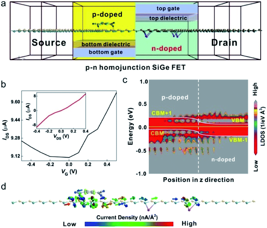 | ||
| Fig. 8 (a) Device architecture of the dual-gated p–n homojunction SiGe FET via the spatially adsorption of F4TCNQ molecule and 4 K atoms. (b) Transfer characteristic of p–n homojunction F4TCNQ-4K/SiGe FET at VDS = 0.4 V. (c) LDOS and (d) current density distribution in the channel region of p–n homojunction F4TCNQ-4K/SiGe FET. | ||
The electrical transfer characteristic of simulated F4TCNQ-4K/SiGe FET is given in Fig. 8b. The device channel was in n-type doping configuration at VG > 0.1 V and in p-type doping configuration at VG < −0.2 V, behaving asymmetrically. Subthreshold swing (SS) lower than 60 mV dec−1 is an important parameter that low-power devices need to meet in ITRS 2028, by which the gate controllability can be evaluated in the subthreshold region.54 SS value of F4TCNQ-4K/SiGe FET is −40.78 mV dec−1 in the subthreshold region of −0.5 V < VG < −0.2 V and 20.52 mV dec−1 in 0.1 V < VG < 0.5 V, respectively, where SS value is defined as SS = dVG/d(log![[thin space (1/6-em)]](https://www.rsc.org/images/entities/char_2009.gif) IDS). It is noted that the SS characteristic in F4TCNQ-4K/SiGe FET is remarkably improved, compared with the case of silicene nanoribbon FETs (264 mV per decade) and indium-doped germanene nanoribbon FETs (39.39 mV per decade).55,56 It is reflected that the surface functionalization with F4TCNQ molecule and K atoms is a feasible method to reduce the power consumption in SiGe FETs with p–n homojunction, according to the demand of low-power devices in 2028. Additionally, the inset of Fig. 8b demonstrates the electrical output characteristic of the device. No rectifying behavior is observed in the relationship between IDS and VDS in the entire VDS range from −0.4 to 0.4 V, which is a typical signal for the ambipolar characteristic of the device.57
IDS). It is noted that the SS characteristic in F4TCNQ-4K/SiGe FET is remarkably improved, compared with the case of silicene nanoribbon FETs (264 mV per decade) and indium-doped germanene nanoribbon FETs (39.39 mV per decade).55,56 It is reflected that the surface functionalization with F4TCNQ molecule and K atoms is a feasible method to reduce the power consumption in SiGe FETs with p–n homojunction, according to the demand of low-power devices in 2028. Additionally, the inset of Fig. 8b demonstrates the electrical output characteristic of the device. No rectifying behavior is observed in the relationship between IDS and VDS in the entire VDS range from −0.4 to 0.4 V, which is a typical signal for the ambipolar characteristic of the device.57
In LDOS of Fig. 8c, it is noteworthy that the conduction band in p-type F4TNCQ/SiGe region shifts downward respective to EF by applying VDS = 0.4 V, meanwhile the valence band in 4K/SiGe region shifts upward, owing to the strong interfacial charge transfer between p-type and n-type doped channels. In other words, the tunneling barrier width in the channel region get narrowed by the dramatic band bending, due to the strong hybridization between the VBM states of F4TNCQ/SiGe and the CBM states of 4K/SiGe. Consequently, electrons can transport efficiently through the channel region, giving rise to a high IDS.
The delocalization of current density on F4TCNQ-4K/SiGe FET in Fig. 8d can not only reflect the pathways for electrons to transport between pairs of atoms, but also embody the introduced scattering centers on SiGe monolayer via surface functionalization. As a vector field, the current density can be projected on different slices along each direction for better visualization.58 The blue arrow indicates a lower current density, whereas the red one denotes a higher current density. In p-type F4TCNQ/SiGe region, a large number of red arrows in the direction of the electrical field are distributed on monolayer SiGe, which contributes to the net current. Nevertheless, many blue arrows pointing to the opposite direction of the electrical field are delocalized on the adsorbed F4TCNQ molecule, on which the electron scattering from the direction of the net current flow severely suppresses the current. Hence, numerous scattering centers are introduced into monolayer SiGe by the adsorption of F4TCNQ molecule. The reasons for this phenomenon are both of the strong interaction of F4TCNQ/SiGe and the large projection area of F4TCNQ molecule. On the contrary, since no arrow exists on the adsorbed K atoms, the carrier scattering on the adsorbed K atoms is negligible. In addition, the current density is much higher on the projection region of K atoms, revealing that the injection of electrons from K atoms to SiGe monolayer can remarkably promote the electronic transport efficiency.
4. Conclusions
In summary, by combining ab initio with quantum transport calculations, we have rationally doped holes/electrons into monolayer SiGe, via surface functionalization with electrophilic/nucleophilic dopants, including F4TCNQ, BV molecules, and K atoms. The electron-donating capability of K atoms is stronger than that of BV molecule on the surface of SiGe monolayer, largely owing to the strong covalent interaction. p-type F4TCNQ/SiGe and n-type 4K/SiGe systems possess enhanced optical absorption peaks in the infrared region, in comparison with pristine SiGe, revealing their great potential in the optoelectronic application. Furthermore, we constructed p–n homojunction SiGe FET, which is composed of physisorbed F4TCNQ molecule and chemisorbed 4 K atoms onto an armchair SiGe nanoribbon. The VBM states of p-type F4TNCQ/SiGe has a strong hybridization with the CBM states of n-type 4K/SiGe, on which electrons can transport efficiently through the channel region. The large projection area of F4TNCQ molecule has injected a large amount of scattering centers on SiGe monolayer, thus impeding electronic transport in the p-type region, whereas the negligible projection area of K atoms is a positive factor to promote the electron transmission in the n-type region. The simulated p–n homojunction F4TCNQ/4K-SiGe FET can achieve a higher current density and a lower SS value that satisfy the ITRS demands for high-performance and low-power devices in 2028. Our work sheds light on the potential application of surface functionalization in building p–n homojunction electronic and optoelectronic nanodevices based on monolayer SiGe.Conflicts of interest
The authors declare no competing financial interest.Acknowledgements
This work was supported by the National Natural Science Foundation of China (Grant No. 51802121, and 51861145202), the Zhejiang Provincial Natural Science Foundation of China (Grant No. LQ20B030012, and LY19B030006), and the Open Project Program of Key Laboratory of Yarn Materials Forming and Composite Processing Technology, Zhejiang Province, Jiaxing University (MTC2020-17).Notes and references
- M. Riordan and L. Hoddeson, IEEE Spectrum, 1997, 34, 46–51 Search PubMed.
- C. H. Lee, G. H. Lee, A. M. van der Zande, W. C. Chen, Y. L. Li, M. Y. Han, X. Cui, G. Arefe, C. Nuckolls, T. F. Heinz, J. Guo, J. Hone and P. Kim, Nat. Nanotechnol., 2014, 9, 676–681 CrossRef CAS PubMed.
- B. W. H. Baugher, H. O. H. Churchill, Y. F. Yang and P. Jarillo-Herrero, Nat. Nanotechnol., 2014, 9, 262–267 CrossRef CAS.
- G. G. Liu, G. X. Zhao, W. Zhou, Y. Y. Liu, H. Pang, H. B. Zhang, D. Hao, X. G. Meng, P. Li, T. Kako and J. H. Ye, Adv. Funct. Mater., 2016, 26, 6822–6829 CrossRef CAS.
- N. Balakrishnan, Z. R. Kudrynskyi, M. W. Fay, G. W. Mudd, S. A. Svatek, O. Makarovsky, Z. D. Kovalyuk, L. Eaves, P. H. Beton and A. Patane, Adv. Opt. Mater., 2014, 2, 1064–1069 CrossRef CAS.
- Y. D. Liu, Y. Q. Cai, G. Zhang, Y. W. Zhang and K. W. Ang, Adv. Funct. Mater., 2017, 27, 1604638 CrossRef.
- M. Zhong, T. Hisatomi, Y. Kuang, J. Zhao, M. Liu, A. Iwase, Q. Jia, H. Nishiyama, T. Minegishi, M. Nakabayashi, N. Shibata, R. Niishiro, C. Katayama, H. Shibano, M. Katayama, A. Kudo, T. Yamada and K. Domen, J. Am. Chem. Soc., 2015, 137, 5053–5060 CrossRef CAS PubMed.
- F. Wu, Q. Li, P. Wang, H. Xia, Z. Wang, Y. Wang, M. Luo, L. Chen, F. S. Chen, J. S. Miao, X. S. Chen, W. Lu, C. X. Shan, A. L. Pan, X. Wu, W. C. Ren, D. Jariwala and W. D. Hu, Nat. Commun., 2019, 10, 4663 CrossRef.
- S. Y. Hu and J. Gao, Adv. Funct. Mater., 2019 DOI:10.1002/adfm.201907003.
- H. W. Park, A. Song, D. Choi, H. J. Kim, J. Y. Kwon and K. B. Chung, Sci. Rep., 2017, 7, 11634 CrossRef PubMed.
- D. Chen, Z. F. Liu, Z. G. Guo, M. N. Ruan and W. G. Yan, ChemSusChem, 2019, 12, 3286–3295 CrossRef CAS PubMed.
- B. B. Lv, Y. W. Tang, S. Y. Lou, Y. L. Xu and S. M. Zhou, J. Mater. Chem. C, 2016, 4, 5416–5423 RSC.
- X. K. Zhang, Q. L. Liao, Z. Kang, B. S. Liu, Y. Ou, J. L. Du, J. K. Xiao, L. Gao, H. Y. Shan, Y. Luo, Z. Y. Fang, P. D. Wang, Z. Sun, Z. Zhang and Y. Zhang, ACS Nano, 2019, 13, 3280–3291 CrossRef CAS PubMed.
- L. Pan, S. B. Wang, J. W. Xie, L. Wang, X. W. Zhang and J. J. Zou, Nano Energy, 2016, 28, 296–303 CrossRef CAS.
- J. W. Chen, S. T. Lo, S. C. Ho, S. S. Wong, T. H. Y. Vu, X. Q. Zhang, Y. D. Liu, Y. Y. Chiou, Y. X. Chen, J. C. Yang, Y. C. Chen, Y. H. Chu, Y. H. Lee, C. J. Chung, T. M. Chen, C. H. Chen and C. L. Wu, Nat. Commun., 2018, 9, 3143 CrossRef PubMed.
- S. M. Wu, X. L. Liu, X. L. Lian, G. Tian, C. Janiak, Y. X. Zhang, Y. Lu, H. Z. Yu, J. Hu, H. Wei, H. Zhao, G. G. Chang, G. Van Tendeloo, L. Y. Wang, X. Y. Yang and B. L. Su, Adv. Mater., 2018, 30, 1802173 CrossRef PubMed.
- G. Lee, S. J. Pearton, F. Ren and J. Kim, Adv. Electron. Mater., 2019, 5, 1800745 CrossRef.
- Y. Jing, X. Tan, Z. Zhou and P. Shen, J. Mater. Chem. A, 2014, 2, 16892–16897 RSC.
- F. F. Xia, S. Y. Xiong, Y. Y. He, Z. B. Shao, X. J. Zhang and J. S. Jie, J. Phys. Chem. C, 2017, 121, 19530–19537 CrossRef CAS.
- Z. Shao, J. Jie, Z. Sun, F. Xia, Y. Wang, X. Zhang, K. Ding and S.-T. Lee, Nano Lett., 2015, 15, 3590–3596 CrossRef CAS PubMed.
- W.-C. Lee, J.-Y. Chen, C.-W. Huang, C.-H. Chiu, T.-Y. Lin and W.-W. Wu, Chem. Mater., 2015, 27, 4216–4221 CrossRef CAS.
- A. N. Hoffman, M. G. Stanford, M. G. Sales, C. Zhang, I. N. Ivanov, S. J. McDonnell, D. G. Mandrus and P. D. Rack, Tuning the electrical properties of WSe2 via O2 plasma oxidation: Towards lateral homojunctions, Report 2053-1583, 2019 Search PubMed.
- S. Kim, J. H. Kim, D. Kim, G. Hwang, J. Baik, H. Yang and S. Cho, 2D Mater., 2017, 4, 024004 CrossRef.
- J.-K. Qin, W.-Z. Shao, C.-Y. Xu, Y. Li, D.-D. Ren, X.-G. Song and L. Zhen, ACS Appl. Mater. Interfaces, 2017, 9, 15583–15591 CrossRef CAS PubMed.
- J. R. McKone, A. P. Pieterick, H. B. Gray and N. S. Lewis, J. Am. Chem. Soc., 2013, 135, 223–231 CrossRef CAS PubMed.
- A. Sannyal, Y. Ahn and J. Jang, Comput. Mater. Sci., 2019, 165, 121–128 CrossRef CAS.
- H. C. Zhou, M. W. Zhao, X. M. Zhang, W. Z. Dong, X. P. Wang, H. X. Bu and A. Z. Wang, J. Phys.: Condens. Matter, 2013, 25, 395501 CrossRef PubMed.
- C. Hu, J. L. Taraci, J. Tolle, M. R. Bauer, P. A. Crozier, I. S. T. Tsong and J. Kouvetakis, Chem. Mater., 2003, 15, 3569–3572 CrossRef CAS.
- Atomistix Toolkit version 2018.06, Synopsys QuantumWise A/S, http://www.quantumwise.com Search PubMed.
- M. Brandbyge, J. L. Mozos, P. Ordejon, J. Taylor and K. Stokbro, Phys. Rev. B: Condens. Matter Mater. Phys., 2001, 65, 165401 CrossRef.
- M. Causá and A. Zupan, Int. J. Quantum Chem., 1994, 52, 633–644 CrossRef.
- J. P. Perdew, K. Burke and M. Ernzerhof, Phys. Rev. Lett., 1996, 77, 3865–3868 CrossRef CAS PubMed.
- M. Schlipf and F. Gygi, Comput. Phys. Commun., 2015, 196, 36–44 CrossRef CAS.
- S. Grimme, J. Comput. Chem., 2006, 27, 1787–1799 CrossRef CAS PubMed.
- H. J. Monkhorst and J. D. Pack, Phys. Rev. B: Solid State, 1976, 13, 5188–5192 CrossRef.
- L. G. Ferreira, M. Marques and L. K. Teles, Phys. Rev. B: Condens. Matter Mater. Phys., 2008, 78, 125116 CrossRef.
- G. A. Petersson, T. G. Tensfeldt and J. A. Montgomery, J. Chem. Phys., 1991, 94, 6091–6101 CrossRef CAS.
- N. A. Bruque, R. R. Pandey and R. K. Lake, Phys. Rev. B: Condens. Matter Mater. Phys., 2007, 76, 205322 CrossRef.
- S. Datta, Electronic transport in mesoscopic systems, Cambridge University Press, Cambridge, 1997 Search PubMed.
- R. G. Quhe, Q. H. Li, Q. X. Zhang, Y. Y. Wang, H. Zhang, J. Z. Li, X. Y. Zhang, D. X. Chen, K. H. Liu, Y. Ye, L. Dai, F. Pan, M. Lei and J. Lu, Phys. Rev. Appl., 2018, 10, 024022 CrossRef CAS.
- V. Shukla, J. Warna, N. K. Jena, A. Grigoriev and R. Ahuja, J. Phys. Chem. C, 2017, 121, 26869–26876 CrossRef CAS.
- B. W. Shi, Y. Y. Wang, J. Z. Li, X. Y. Zhang, J. H. Yan, S. Q. Liu, J. Yang, Y. Y. Pan, H. Zhang, J. B. Yang, F. Pan and J. Lu, Phys. Chem. Chem. Phys., 2018, 20, 24641–24651 RSC.
- P. Jamdagni, A. Kumar, A. Thakur, R. Pandey and P. K. Ahluwalia, Mater. Res. Express, 2015, 2, 016301 CrossRef.
- H. He, K. H. Kim, A. Danilov, D. Montemurro, L. Y. Yu, Y. W. Park, F. Lombardi, T. Bauch, K. Moth-Poulsen, T. Lakimov, R. Yakimova, P. Malmberg, C. Muller, S. Kubatkin and S. Lara-Avila, Nat. Commun., 2018, 9, 3956 CrossRef PubMed.
- Y. Y. He, F. F. Xia, Z. B. Shao, J. W. Zhao and J. S. Jie, J. Phys. Chem. Lett., 2015, 6, 4701–4710 CrossRef CAS PubMed.
- J. M. Yuan, C. Tang, J. X. Zhong and Y. L. Mao, Appl. Surf. Sci., 2016, 360, 707–714 CrossRef CAS.
- T. Ahmed, H. Sakib and S. Subrina, Nanotechnology, 2020, 31, 035701 CrossRef.
- C. J. Zhou, W. H. Yang and H. L. Zhu, J. Chem. Phys., 2015, 142, 214704 CrossRef PubMed.
- A. C. Bevilacqua, M. H. Köhler, S. Azevedo and R. J. Baierle, Phys. Chem. Chem. Phys., 2017, 19, 5629–5636 RSC.
- Q. Zhang, T. Y. Xin, X. K. Lu and Y. X. Wang, Materials, 2018, 11, 431 CrossRef PubMed.
- Y. Y. Jin, Z. Y. Zeng, Z. W. Xu, Y. C. Lin, K. X. Bi, G. L. Shao, T. S. Hu, S. S. Wang, S. S. Li, K. Suenaga, H. G. Duan, Y. X. Feng and S. Liu, Chem. Mater., 2019, 31, 3534–3541 CrossRef CAS.
- J. H. Yan, H. Pang, L. Xu, J. Yang, R. G. Quhe, X. Y. Zhang, Y. Y. Pan, B. W. Shi, S. Q. Liu, L. Q. Xu, J. B. Yang, F. Pan, Z. Y. Zhang and J. Lu, Adv. Electron. Mater., 2019, 5, 1900226 CrossRef.
- Y. Y. Wang, R. X. Fei, R. Quhe, J. Z. Li, H. Zhang, X. Y. Zhang, B. W. Shi, L. Xiao, Z. G. Song, J. B. Yang, J. J. Shi, F. Pan and J. Lu, ACS Appl. Mater. Interfaces, 2018, 10, 23344–23352 CrossRef CAS PubMed.
- J. Wang, Q. Cai, J. Lei, G. Yang, J. Xue, D. Chen, B. Liu, H. Lu, R. Zhang and Y. Zheng, ACS Appl. Mater. Interfaces, 2019, 11, 20956–20964 CrossRef CAS PubMed.
- H. Li, L. Wang, Q. H. Liu, J. X. Zheng, W. N. Mei, Z. X. Gao, J. J. Shi and J. Lu, Eur. Phys. J. B, 2012, 85, 274 CrossRef.
- S. Singh, K. Garg, A. Sareen, R. Mehla and I. Kaur, Org. Electron., 2018, 54, 261–269 CrossRef CAS.
- J. Baltazar, H. Sojoudi, S. A. Paniagua, J. Kowalik, S. R. Marder, L. M. Tolbert, S. Graham and C. L. Henderson, J. Phys. Chem. C, 2012, 116, 19095–19103 CrossRef CAS.
- L. Zhang, B. Wang and J. Wang, Phys. Rev. B: Condens. Matter Mater. Phys., 2012, 86, 165431 CrossRef.
Footnote |
| † Electronic supplementary information (ESI) available. See DOI: 10.1039/d0ra01218a |
| This journal is © The Royal Society of Chemistry 2020 |