
 Open Access Article
 This Open Access Article is licensed under a Creative Commons Attribution-Non Commercial 3.0 Unported Licence
Boosting performances of triboelectric nanogenerators by optimizing dielectric properties and thickness of electrification layer†
Xiaofang Kangab,
Chongxiang Panac,
Yanghui Chenab and
Xiong Pu *abc
*abc
aCAS Center for Excellence in Nanoscience, Beijing Key Laboratory of Micro-Nano Energy and Sensor, Beijing Institute of Nanoenergy and Nanosystems, Chinese Academy of Sciences, Beijing 100083, China. E-mail: puxiong@binn.cas.cn
bSchool of Nanoscience and Technology, University of Chinese Academy of Sciences, Beijing 100049, China
cCenter on Nanoenergy Researh, School of Chemistry and Chemical Engineering, School of Physical Science and Technology, Guangxi University, Nanning 530004, China
First published on 6th May 2020
Abstract
Triboelectric nanogenerators (TENGs) with excellent flexibility and high outputs are promising for powering wearable/wireless electronics with electricity converted from ubiquitous mechanical energies in the working environment. In this work, the effects of the dielectric properties and thickness of the electrification film on the performance of the TENG are discussed. BaTiO3 nanoparticles are added into poly(vinylidene fluoride) (PVDF) to improve the dielectric constant of the composite film. The TENG using a BaTiO3/PVDF nanocomposite film with 11.25 vol% BaTiO3 as the tribo-negative electrification layer is demonstrated to be the optimized one, and generates an open-circuit voltage of 131 V and transferred short-circuit charge density of 89 μC m−2, 6.5 fold higher than those of a TENG using bare a PVDF layer. Furthermore, by reducing the thickness of the BaTiO3/PVDF film to 5 μm, the voltage and charge density increase to 161 V and 112 μC m−2, respectively, and an instantaneous peak power density of 225.6 mW m−2 is obtained.
1. Introduction
The rapid advancement of miniaturized electronic devices has led to their extensive applications in wireless, portable, wearable and distributed smart devices. Nevertheless, the green energy resource to provide sustainable power for these devices has always been a major concern. Harvesting ubiquitous mechanical energies from the working environments of electronic devices has been proven to be one of the most promising strategies. Among various energy harvesting technologies, triboelectric nanogenerators (TENGs),1 based on the coupling of triboelectrification and electrostatic induction,2 have emerged as a promising technique to convert mechanical energy into electricity due to their high output voltage, simple fabrication,3 flexibility and low cost.4–7 As an energy harvester, further enhancing the output performance is critical to speed up their practical applications.There have been many reports on improving the output power of TENGs. Several strategies have been developed, such as the device structure optimization,8–10 excitation circuit,11,12 vacuum environment,13 and corona charge bombardment.14–16 From a materials perspective, optimizing the tribo-electrification film is essential. By increasing the effective contact area, the tribo-electrified static surface charge density can be improved. Many methods have been utilized to enlarge the effective contact area, such as plasma etching,17 electrospinning technique,18–20 as well as the use of silicon mold for pattern transfer.21,22 Alternatively, surface modification is adopted to tune the tribo-negativity of a dielectric film, so as to improve the generated static charge density. Improving the dielectric properties of triboelectric materials is also an effective method. Zhai et al.23 have improved the performances of TENG by adding titania monolayer to poly(vinylidene fluoride) (PVDF) to improve dielectric constant. Lee et al.24 synthesized PtBA-grafted PVDF copolymers with high dielectric constant, which improved TENG's performance several times. Inorganic fillers with high dielectric constant or conductive fillers were also reported to be embedded in the polymer matrix, such as carbon nanotubes,25 graphene,19 ceramic materials,26–29 and metal–organic framework materials.30 Other than these properties, the thickness of the electrification layer can also affect the output performances, but its effect is not well studied experimentally.
In this work, dielectric properties and thickness of the tribo-electrification film were optimized to improve the output performances of TENG. BaTiO3 nanoparticles were added into a PVDF polymer matrix. BaTiO3/PVDF nanocomposite film showed enhanced output performances when it was employed as a negative triboelectric layer in a two-electrode TENG. The volume fraction of the BaTiO3 was optimized, and the BaTiO3/PVDF composite film with 11.25 vol% BaTiO3 filler (40 μm thick) generated open-circuit voltage of 131 V and transferred short-circuit charge density of 89 μC m−2, 6.5 folds higher than TENG using bare PVDF. Furthermore, by reducing the thickness of BaTiO3/PVDF film to 5 μm, the voltage and charge density increased further to 161 V and 112 μC m−2, respectively. The electrification layer of 5 μm BaTiO3/PVDF composite film generated a peak power density of 225.6 mW m−2 at a load resistance of 100 MΩ. The device was used for charging commercial capacitors and glowing LEDs. Furthermore, the enhanced output performance of the 5 μm composite film-based TENG shows good stability and durability under continuous operation of 4000 cycles.
2. Experimental section
2.1 Materials
Poly(vinylidene fluoride) (PVDF) powder was provided by Arkema. N,N-Dimethylformamide (DMF) was purchased from Tianjin yongda (China). Tetragonal piezoelectric barium titanate (BaTiO3) nanoparticles, with an average diameter of 100 nm, were obtained from Sigma-Aladdin. The XRD curve and SEM image of BaTiO3 nanoparticles were shown in Fig. 1b and c. All chemicals were used as received without further purification.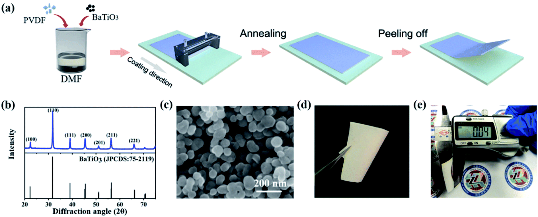 | ||
| Fig. 1 (a) Scheme of the fabrication process of the BaTiO3/PVDF nanocomposite films. (b) The XRD patterns of BaTiO3 nanoparticles compared to BaTiO3 standard data (JPCDS: 75-2119). (c) The SEM image of BaTiO3 particles. (d) The photo shows the bendability of the BaTiO3/PVDF nanocomposite films. (e) The thickness of the films. | ||
2.2 Preparation of BaTiO3/PVDF composite film
The PVDF powder was dissolved in DMF with the density 0.1 g ml−1 and vigorously stirred several days to obtain a homogeneous solution. The different volume fraction of BaTiO3 particles (3.18–16.47 vol%) were mixed in the PVDF solution, and the solution was ultrasonic treated for 3 h and stirred 24 h to improve the dispersion of the particles. Correspondingly, the bare PVDF solution was made as to the comparative experiment. The BaTiO3/PVDF nanocomposite films were prepared by the doctor-blade casting method, dried at 60 °C for 4 h in an oven, and then peeled off from the substrates.2.3 Characterization of BaTiO3/PVDF composite film
Field-emission scanning electron microscopy (SEM, Nova) was used to characterize the thickness of BaTiO3/PVDF films and the distribution of BaTiO3 nanoparticles in the polymer. X-ray diffraction was collected on a Panalytical Instrument X'Pert 3 Power with Cu Kα radiation source. Fourier transform infrared (ATR-FTIR) spectra of PVDF and BaTiO3/PVDF composite films were detected by TENSOR II spectrometer (BRUKER, German).The dielectric constant was measured by Keysight (E4980A) at frequencies ranging from 103 Hz to 106 Hz at room temperature. Prior to the experiment, all the films were cut into a round with a diameter of 20 mm and their thickness was measured, then copper was plated on each side of the films by magnetron sputtering.
2.4 Fabrication of the contact-separation TENGs
The TENG device was fabricated into a vertical contact-separation structure with a simple two-electrode system and the effective area was 2 × 2 cm2. The positive friction layer of the nanogenerator is made of nylon; the copper tape was pasted on nylon to act as one electrode. The tribo-negative BaTiO3/PVDF nanocomposite films were first sputtering-coated with Cu (100 nm) for using as another electrode. Then, the Cu side was attached on a 3 M foam tape and stacked to an acrylic substrate. The 3 M foam tape is used to fix the electrodes and to buffer the impact. Lastly, conducting wires were connected to the two Cu electrodes through external circuit for measurement.The two electrification layers are subjected to contact-separation motions provided by a linear motor, and the output voltage signals and output current signals of the as-fabricated TENG were measured by a Keithley 6514 electrometer.
3. Results and discussion
The schematic diagram of the fabrication process for the BaTiO3/PVDF nanocomposite films is shown in Fig. 1a. BaTiO3 nanoparticles were mixed with PVDF in the DMF solvent, followed by preparing the composite film with a doctor-blade casting method. The XRD patterns of BaTiO3 nanoparticles were shown in Fig. 1b. The XRD peaks suggested that BaTiO3 has a tetragonal phase,31 indicating appreciable ferroelectricity.32 It can be seen from Fig. 1c that the diameter of BaTiO3 nanoparticles is uniformly about 100 nanometers. After removing the nanocomposite films from the substrate, it can be seen that it is white and quite flexibility (Fig. 1d). The thickness of BaTiO3/PVDF nanocomposite films was controlled to be about 40 μm, as seen from Fig. 1e. The volume fraction of the BaTiO3 was varied (3.18–16.47 vol%) and a bare PVDF film was also prepared for comparison.The XRD patterns of BaTiO3/PVDF nanocomposite films with BaTiO3 content of 0 vol%–16.47 vol% are shown in Fig. S1a.† With the increase of BaTiO3 fillers, the peaks of PVDF become weaker, but the intensity of BaTiO3 peaks increases. The FTIR spectra of bare PVDF and BaTiO3/PVDF nanocomposite with different concentrations of BaTiO3 have been carried out (Fig. S1b†). The data implied that there is no significant phase change in crystalline phases when changing the BaTiO3 volume fraction. The results suggest that the adding of BaTiO3 nanoparticles had negligible effect on the crystalline structure of polymer matrix.
The thickness of PVDF and all BaTiO3/PVDF films were measured by the cross-sectional scanning electron microscopy (SEM) images, as shown in Fig. 2a and S2.† It is clear that the thickness of all films was approximately about 40 μm. From the surface morphologies of the bare PVDF and nanocomposite films in Fig. 2b and S3,† it can be seen that BaTiO3 nanoparticles were dispersed uniformly in the matrix, indicating good compatibility between BaTiO3 nanoparticles and the PVDF. The energy dispersive spectroscopy (EDS) mapping (Fig. S4†) also showed that all the elements are evenly distributed throughout the nanocomposite films. We used the atomic force microscope (AFM) to evaluate the surface topography of the BaTiO3/PVDF films, as shown in Fig. 2c. It can be observed that the surface roughness increases with increasing in BaTiO3 content.
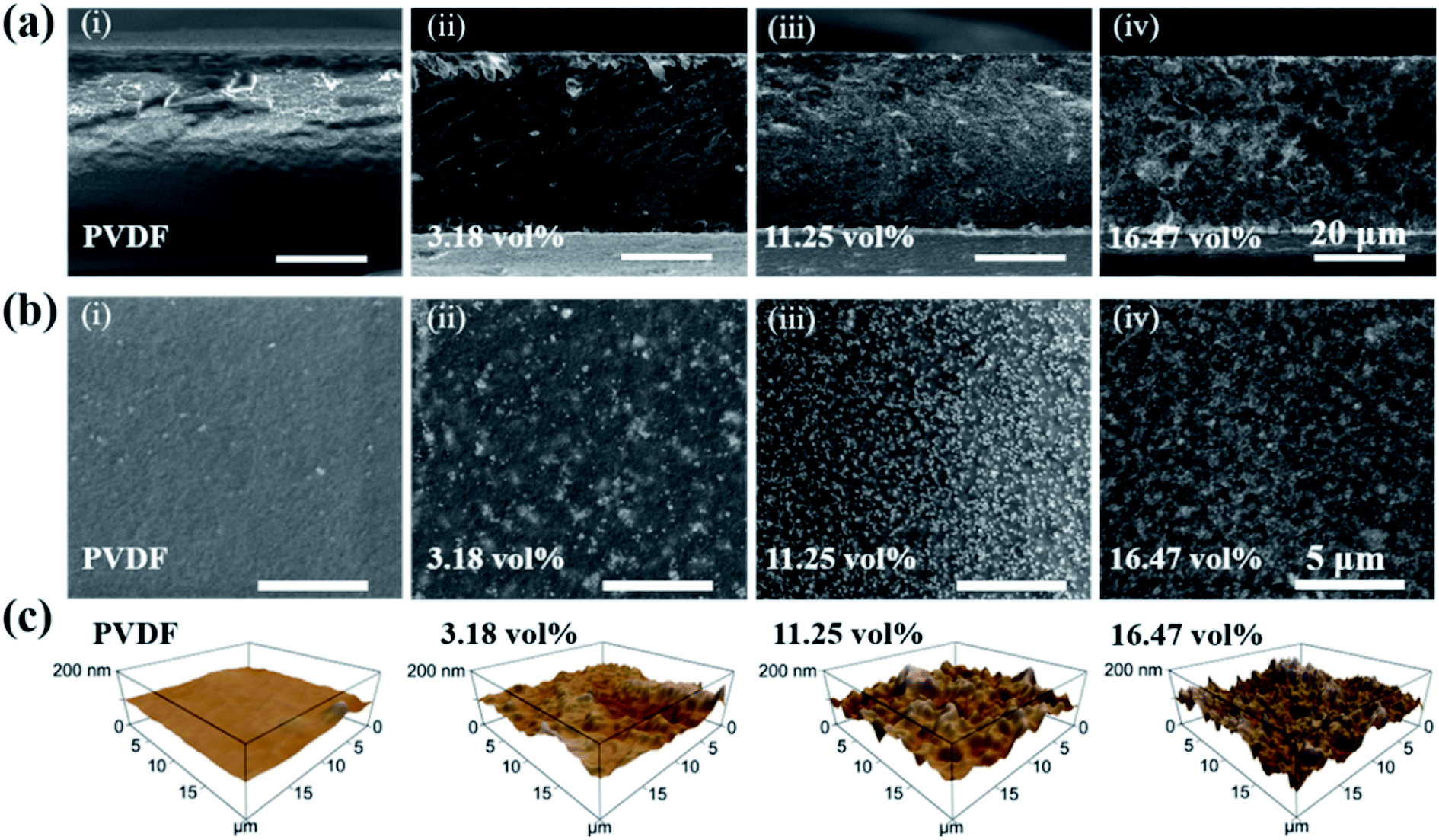 | ||
| Fig. 2 SEM and AFM images of the BaTiO3/PVDF films. (a) Cross-sectional and (b) surface morphology SEM images for composite films with different BaTiO3 volume fractions. (c) 3-dimensional AFM images of the composite films. | ||
The dielectric properties for the PVDF and BaTiO3/PVDF nanocomposite films were further measured at room temperature, as shown in Fig. 3a. The PVDF displayed a dielectric constant of 7.96 at 1000 Hz, which is basically consistent with previous reports.33,34 It is clear that the dielectric constant increased with the increase of the BaTiO3 volume fraction, owing to the higher dielectric constant of BaTiO3 compared to bare PVDF. The dielectric constant of the 11.25 vol% and 16.47 vol% BaTiO3/PVDF films is as high as 25 and 29, respectively.
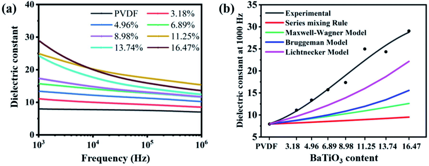 | ||
| Fig. 3 (a) Frequency dependence of dielectric constant values for composite films with different BaTiO3 volume fractions from 0 to 16.47 vol%. (b) Comparison of experimental and theoretical dielectric constant at 1000 Hz of BaTiO3/PVDF films. | ||
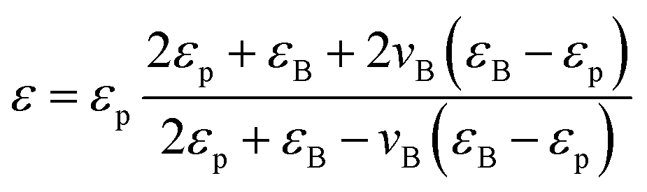
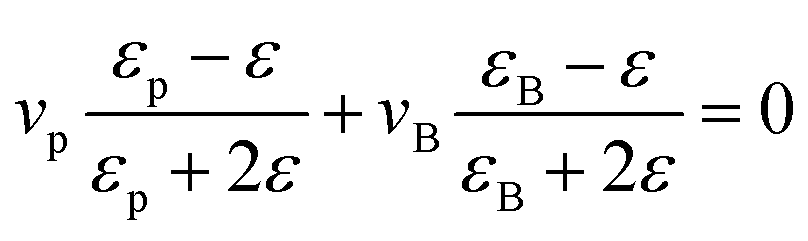
To better understand the dielectric behavior of the BaTiO3/PVDF composite films, several theoretical models have been employed and comparisons have been done between the experimental and theoretical values (Fig. 3b). The following equations are used of calculate the values of dielectric constant of the nanocomposites:
(i) Series mixing equation:35
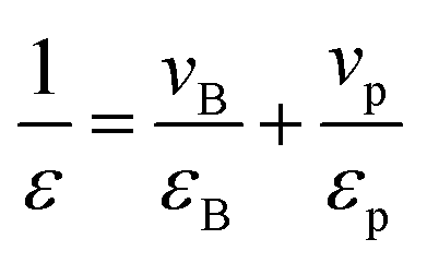 | (1) |
 | (2) |
 | (3) |
ln![[thin space (1/6-em)]](https://www.rsc.org/images/entities/char_2009.gif) ε = vBlnεB + vplnεp ε = vBlnεB + vplnεp
| (4) |
A two-electrode TENG was fabricated for evaluating the electrification properties of the composite films, as shown in Fig. 4a. The composite film was employed as a triboelectric negative layer and a nylon film was used as the tribo-positive layer. The contact effective area is fixed to be 2 × 2 cm2. An as-fabricated TENG device is shown in Fig. S6.† The working mechanism of the contact-separation mode TENG is schematically illustrated in Fig. 4b.39–41 When the nylon film contacts with the BaTiO3/PVDF film (Fig. 4b-i), tribo-electrification occurs with static charges generated at two tribo-materials surfaces with opposite signs because of their differences in work function. According to the triboelectric series table,42 PVDF will be negatively charged and the nylon will be positively charged. When the two layers begin to separate from each other (Fig. 4b-ii), the electron will flow from the top Cu electrode to the bottom electrode through the external circuit, so as to achieve local charge equilibrium, i.e. the process of static induction. If at open-circuit state, the unscreened charges will induce a potential difference between the two Cu electrodes. Once the two triboelectric layers are far away enough (the maximum transferred charges can be achieved at a separation distance about ∼ 1 mm43,44), charge equilibrium will be achieved and the charge transfer through the external circuit will be finished (Fig. 4b-iii). As the top layer begins to be compressed again (Fig. 4b-iv), electrons are driven to flow from the bottom electrode to the top electrode, yielding an electrical output signal with an opposite sign. Finally, when the device is fully compressed (Fig. 4b-i), the balance in electric charge is retained, completing one cycle of electricity generation. Repeating the compress-release motions, mechanical motions are converted into pulsed AC currents. The built-up potential difference between the two electrodes at open-circuit condition can be confirmed by the finite-element simulation using the COMSOL Multiphysics software, as shown in Fig. S7.† We performed the surface potential distribution at the contact state to the maximum release state. At contact state (5 μm gap distance between the Nylon and PVDF film), the top and bottom surface has no potential difference. When the distance is 1 mm, a large potential difference between the two surfaces can be observed and a surface charge density of 15 μC m−2 is obtained.
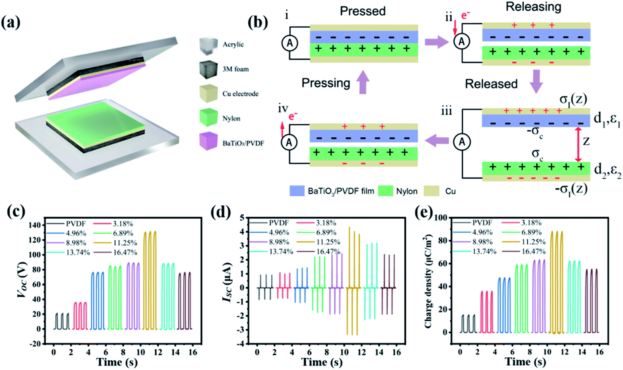 | ||
| Fig. 4 Triboelectric performances of the TENG. (a) Schematic structural components of the TENG device. (b) Working mechanism of the contact-separation mode TENG. The harvested (c) output voltage, (d) current and (e) transferred charge density signals of TENG based the BaTiO3/PVDF films. | ||
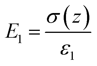
As shown in Fig. 4b-iii, ε1 and ε2 are the dielectric constant of the BaTiO3/PVDF film and the nylon, respectively; d1 and d2 are the thicknesses of the BaTiO3/PVDF film and the nylon, respectively. The gap z can be varied under mechanical motions. After several cycles of contacting, the surface static charge areal density σc reaches saturation. When the z is increased, a potential difference (V) induced by the triboelectric charges drives electrons to flow through the external load, leading to the accumulation of free electrons in the electrode45 (i.e. transferred charge density, σ(z)). The electric fields in the two tribo-material layers and in the gap are given by:46
 | (5) |
 | (6) |
 | (7) |
| V = σ(z)[d1/ε1 + d2/ε2] + z[σ(z) − σc]/ε0 | (8) |
Under open-circuit condition, the transferred charge density σ(z) = 0, the open-circuit voltage can be described as:
| Voc = −zσc/ε0 | (9) |
Under short-circuit condition, the voltage between the two electrodes is zero. Then, the σ(z) can be derived as
 | (10) |
The σ(z) saturates at a maximum separation distance of about 1 mm.43 According to eqn (10), σ(z) is proportional to the dielectric constant of the tribo-material layers and inversely proportional to the thickness of tribo-material layers. So, to get larger σ(z), we should enlarge dielectric constant but decrease the thickness of the electrification layer.
The open-circuit voltage (Voc), short-circuit current (Isc) and transferred charge density (σ(z)) of the TENGs were recorded. To evaluate the effects of BaTiO3 fillers, the thickness of BaTiO3/PVDF film and nylon film, contact force (12 N), and speed (1 m s−1) are all fixed to be the same. The electrical output Voc, Isc and σ(z) of TENGs based on the bare PVDF film and BaTiO3/PVDF nanocomposites films were shown in Fig. 4c–e, respectively. The Voc of TENG was increased from 20 V to nearly 132 V as the filler concentration of BaTiO3 was varied from 0 to 11.25 vol%. At the same time, the Isc and σ(z) of the TENG were enhanced from ≈0.9 to 4.1 μA and ≈15 to 88 μC m−2, respectively. When the filler concentration of BaTiO3 was further increased, the Voc, Isc and σ(z) values of TENG showed an obvious decrease. The Voc values of TENG dropped to nearly 76 V, by increasing the filler concentration of BaTiO3 to 16.47 vol%. The Isc and σ(z) values were decreased to ≈2.3 μA and ≈55.2 μC m−2, respectively. Results reveal that output performance tends to increase with the BaTiO3 volume fraction below 11.25 vol%; further increasing the BaTiO3 concentration, the output performances began to decline.
As shown in Fig. 2a and S2,† the thickness of the PVDF and all BaTiO3/PVDF nanocomposite films are about the same, which implies that the effect of the thickness on the output performances is negligible. The improvement of the output performances can be largely attributed to the increase in the dielectric constant of the composite films, in accordance with eqn (10). However, it is still needed to explain the decrease of the output performances when the BaTiO3 volume fraction is larger than 11.25 vol%. According to the previous works,47,48 increasing the film's roughness is an important way to enhance the output signals of TENG, due to the more generated static charge densities (σc) by increasing the effective contact areas for electrification. However, there are trade-off effects of the BaTiO3 fillers on the static charge densities. As shown by the surface SEM images in Fig. 2b and S3,† the areal fraction of exposed BaTiO3 nanoparticles on the surface will also increase with their volume fraction. As PVDF (high tribo-negativity in tribo-series table) is a much better tribo-electrification material than inorganic BaTiO3, the decrease of the PVDF matrix surface area can also lead to the decrease in generated static charge σc. Therefore, there is an optimum volume fraction of BaTiO3, above which the static charge σc and the output performances of the TENG will decrease. This is accordant with the variation trend of the measured performances, and the optimized BaTiO3 volume fraction is 11.25 vol%.
Since the BaTiO3 volume fraction is optimized to be 11.25 vol%, the output performances can be further enhanced by decreasing the thickness of the composite film. Therefore, we fixed the concentration of BaTiO3 to be 11.25 vol%, and prepared composite films of different thicknesses. Four films of different thickness were prepared (5 μm, 26 μm, 31 μm, 45 μm), as shown in Fig. 5a, and the thickness of Nylon is fixed at 10 μm (Fig. S8†). It was clearly observed that the output transferred charge densities dramatically increase with the decrease of the thickness (Fig. 5d). When a 5 μm BaTiO3/PVDF nanocomposite film was used as the negative electrification layer, the output performance reaches the maximum. The Voc, Isc and σ(z) are 160 V, 6.2 μA and 114 μC m−2 (Fig. 5b–d), respectively, correspondent to 180%, 270%, and 200% improvement comparing with that using 45 μm thick electrification layer. Besides, the instantaneous power density and current density of 5 μm thick-based TENG was obtained (Fig. 5e). As the resistance increases, the current density decreases and the output power density increases first and then decreases. The maximum power density reaches 225.6 mW m−2 at a load resistance of 100 MΩ.
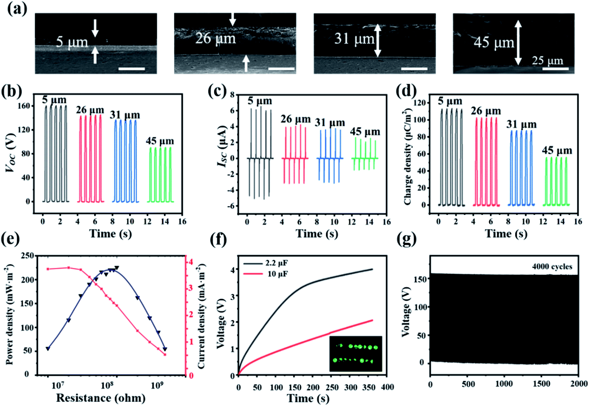 | ||
| Fig. 5 (a) Cross-sectional SEM images of different thicknesses with 11.25 vol% BaTiO3/PVDF composite films. (b) The open-circuit voltage, (c) short-circuit current and (d) transferred charge density of different thickness 11.25 vol% BaTiO3/PVDF-based TENGs. (e) The output current density and power density of TENG based on the 5 μm BaTiO3/PVDF nanocomposite films with 11.25 vol% of BaTiO3. (f) Lightening LEDs and charging commercial capacitors by the TENG. (g) The stability test of the TENG. | ||
To show that capability of TENG as a power source, commercial capacitors have been charged by the TENG. Rectifying circuit is used to convert the generated AC current into DC current to charge commercial capacitors. The 2 μF and 10 μF capacitors can be charged to about 4 V and 2 V in 6 min, respectively. 16 LEDs connected in series can also be lightened by the TENG (Fig. 5f). Lastly, the 5 μm composite film-based TENG shows stable output performances for over 4000 cycles of repeated testes, suggesting the good stability and durability (Fig. 5g). It is noted that rigid the acrylic is used as the substrate for the convenience of the measurement. However, the device can certainly be more flexible if flexible substrate is used for substrate.
4. Conclusion
In summary, we report an effective approach to improve the performances of a TENG through increasing the dielectric constant and decreasing the thickness of the electrification layer. BaTiO3 nanoparticles were added into the PVDF matrix. The dielectric constant of the BaTiO3/PVDF composite increases with the BaTiO3 content. As the BaTiO3 concentration increased to 11.25 vol%, the dielectric constant values raised from 7.96 to 25 at 1000 Hz. Though the output performances of the TENG are positively proportional to the dielectric constant of the composite, the generated static charges could decrease at higher filler content. Therefore, the optimized BaTiO3 content is determined to be 11.25 vol%, which shows a five-fold enhancement in transferred charge density compared to bare PVDF-based TENG. By further decreasing the thickness of composite films to 5 μm, the Qsc increases to 114 μC m−2, corresponding to 200% improvement compared to the TENG with 45 μm thick composite electrification layer. The enhanced output performance of the 5 μm composite film-based TENG shows good stability and durability.Conflicts of interest
The authors declare that they have no conflict of interest.Acknowledgements
The authors thank for the support from National Natural Science Foundation of China (Grant No. 51603013), and the Youth Innovation Promotion Association of CAS.References
- F. R. Fan, Z. Q. Tian and Z. L. Wang, Nano Energy, 2012, 1, 328–334 CrossRef CAS.
- N. Simiao, L. Ying, Z. Yu Sheng, W. Sihong, L. Long and W. Zhong Lin, IEEE Trans. Electron Devices, 2015, 62, 641–647 Search PubMed.
- A. Chandrasekhar, G. Khandelwal, N. R. Alluri, V. Vivekananthan and S.-J. Kim, ACS Sustainable Chem. Eng., 2018, 6, 6110–6116 CrossRef CAS.
- S. Wang, L. Lin and Z. L. Wang, Nano Energy, 2015, 11, 436–462 CrossRef CAS.
- X. Pu, M. Liu, X. Chen, J. Sun, C. Du, Y. Zhang, J. Zhai, W. Hu and Z. L. Wang, Sci. Adv., 2017, 3, e1700015 CrossRef PubMed.
- Y. Chen, X. Pu, M. Liu, S. Kuang, P. Zhang, Q. Hua, Z. Cong, W. Guo, W. Hu and Z. L. Wang, ACS Nano, 2019, 13, 8936–8945 CrossRef CAS PubMed.
- A. Chandrasekhar, V. Vivekananthan, G. Khandelwal and S. J. Kim, Nano Energy, 2019, 60, 850–856 CrossRef CAS.
- S. Wang, L. Lin and Z. L. Wang, Nano Lett., 2012, 12, 6339–6346 CrossRef CAS PubMed.
- G. Zhu, J. Chen, T. Zhang, Q. Jing and Z. L. Wang, Nat. Commun., 2014, 5, 3426 CrossRef PubMed.
- W. Ding, J. Sun, G. Chen, L. Zhou, J. Wang, X. Gu, J. Wan, X. Pu, B. Tang and Z. L. Wang, J. Mater. Chem. C, 2019, 7, 10769–10776 RSC.
- L. Xu, T. Z. Bu, X. D. Yang, C. Zhang and Z. L. Wang, Nano Energy, 2018, 49, 625–633 CrossRef CAS.
- L. Cheng, Q. Xu, Y. Zheng, X. Jia and Y. Qin, Nat. Commun., 2018, 9, 3773 CrossRef PubMed.
- J. Wang, C. Wu, Y. Dai, Z. Zhao, A. Wang, T. Zhang and Z. L. Wang, Nat. Commun., 2017, 8, 88 CrossRef PubMed.
- T. Zhou, L. Zhang, F. Xue, W. Tang, C. Zhang and Z. L. Wang, Nano Res., 2016, 9, 1442–1451 CrossRef CAS.
- B. D. Chen, W. Tang, C. Zhang, L. Xu, L. P. Zhu, L. J. Yang, C. He, J. Chen, L. Liu, T. Zhou and Z. L. Wang, Nano Res., 2018, 11, 3096–3105 CrossRef CAS.
- J. Zhong, Q. Zhong, G. Chen, B. Hu, S. Zhao, X. Li, N. Wu, W. Li, H. Yu and J. Zhou, Energy Environ. Sci., 2016, 9, 3085–3091 RSC.
- H. Y. Li, L. Su, S. Y. Kuang, C. F. Pan, G. Zhu and Z. L. Wang, Adv. Funct. Mater., 2015, 25, 5691–5697 CrossRef CAS.
- G. Q. Gu, C. B. Han, C. X. Lu, C. He, T. Jiang, Z. L. Gao, C. J. Li and Z. L. Wang, ACS Nano, 2017, 11, 6211–6217 CrossRef CAS PubMed.
- K. Shi, B. Sun, X. Huang and P. Jiang, Nano Energy, 2018, 52, 153–162 CrossRef CAS.
- H. Oh, S. S. Kwak, B. Kim, E. Han, G. H. Lim, S. W. Kim and B. Lim, Adv. Funct. Mater., 2019, 29, 1904066 CrossRef.
- D. Tantraviwat, P. Buarin, S. Suntalelat, W. Sripumkhai, P. Pattamang, G. Rujijanagul and B. Inceesungvorn, Nano Energy, 2020, 67, 104214 CrossRef CAS.
- V. Vivekananthan, A. Chandrasekhar, N. R. Alluri, Y. Purusothaman and S.-J. Kim, Nanoscale Adv., 2020, 2, 746–754 RSC.
- R. Wen, J. Guo, A. Yu, K. Zhang, J. Kou, Y. Zhu, Y. Zhang, B.-W. Li and J. Zhai, Nano Energy, 2018, 50, 140–147 CrossRef CAS.
- J. W. Lee, H. J. Cho, J. Chun, K. N. Kim, S. Kim, C. W. Ahn, I. W. Kim, J. Y. Kim, S. W. Kim, C. Yang and J. M. Baik, Sci. Adv., 2017, 3, e1602902 CrossRef PubMed.
- H. Wang, M. Shi, K. Zhu, Z. Su, X. Cheng, Y. Song, X. Chen, Z. Liao, M. Zhang and H. Zhang, Nanoscale, 2016, 8, 18489–18494 RSC.
- S. Hajra, S. Sahoo, M. De, P. K. Rout, H. S. Tewari and R. N. P. Choudhary, J. Mater. Sci.: Mater. Electron., 2017, 29, 1463–1472 CrossRef.
- S. Hajra, S. Sahoo and R. N. P. Choudhary, J. Polym. Res., 2018, 26(1), 14 CrossRef.
- S. Hajra, S. Sahoo, R. Das and R. N. P. Choudhary, J. Alloys Compd., 2018, 750, 507–514 CrossRef CAS.
- S. K. Barik, S. Nath, S. Hajra and R. N. P. Choudhary, Mod. Phys. Lett. B, 2019, 33, 1950352 CrossRef CAS.
- S. Xie, J.-Y. Hwang, X. Sun, S. Shi, Z. Zhang, Z. Peng and Y. Zhai, J. Power Sources, 2014, 253, 132–137 CrossRef CAS.
- A. Li, C. Ge, P. Lü, D. Wu, S. Xiong and N. Ming, Appl. Phys. Lett., 1997, 70, 1616–1618 CrossRef CAS.
- K. Shi, X. Huang, B. Sun, Z. Wu, J. He and P. Jiang, Nano Energy, 2019, 57, 450–458 CrossRef CAS.
- H. Luo, Z. Wu, C. Chen, C. Ma, K. Zhou and D. Zhang, Composites, Part A, 2016, 86, 57–65 CrossRef CAS.
- Y. Xie, J. Wang, Y. Yu, W. Jiang and Z. Zhang, Appl. Surf. Sci., 2018, 440, 1150–1158 CrossRef CAS.
- C. P. Wong, T. Marinis, Q. Jianmin and R. Yang, IEEE Trans. Compon. Packag. Technol., 2000, 23, 680–683 CrossRef.
- J.-G. Hyun, S.-D. Cho and K.-W. Paik, J. Electron. Mater., 2005, 34, 1264–1269 CrossRef CAS.
- S. Dash, R. N. P. Choudhary, A. Kumar and M. N. Goswami, J. Mater. Sci.: Mater. Electron., 2019, 30, 19309–19318 CrossRef CAS.
- N. Jayasundere and B. V. Smith, J. Appl. Phys., 1993, 73, 2462–2466 CrossRef.
- G. Zhu, Z. H. Lin, Q. Jing, P. Bai, C. Pan, Y. Yang, Y. Zhou and Z. L. Wang, Nano Lett., 2013, 13, 847–853 CrossRef CAS PubMed.
- J. Wang, Z. Wen, Y. Zi, P. Zhou, J. Lin, H. Guo, Y. Xu and Z. L. Wang, Adv. Funct. Mater., 2016, 26, 1070–1076 CrossRef CAS.
- K. Dong, Z. Wu, J. Deng, A. C. Wang, H. Zou, C. Chen, D. Hu, B. Gu, B. Sun and Z. L. Wang, Adv. Mater., 2018, 30, e1804944 CrossRef PubMed.
- Z. L. Wang and A. C. Wang, Mater. Today, 2019, 30, 34–51 CrossRef CAS.
- S. Niu, S. Wang, L. Lin, Y. Liu, Y. S. Zhou, Y. Hu and Z. L. Wang, Energy Environ. Sci., 2013, 6, 3576 RSC.
- S. Niu and Z. L. Wang, Nano Energy, 2015, 14, 161–192 CrossRef CAS.
- M. Lai, B. Du, H. Guo, Y. Xi, H. Yang, C. Hu, J. Wang and Z. L. Wang, ACS Appl. Mater. Interfaces, 2018, 10, 2158–2165 CrossRef CAS PubMed.
- Z. L. Wang, T. Jiang and L. Xu, Nano Energy, 2017, 39, 9–23 CrossRef CAS.
- G. Yao, L. Xu, X. Cheng, Y. Li, X. Huang, W. Guo, S. Liu, Z. L. Wang and H. Wu, Adv. Funct. Mater., 2019, 30(6), 1907312 CrossRef.
- J. Chen, H. Guo, X. He, G. Liu, Y. Xi, H. Shi and C. Hu, ACS Appl. Mater. Interfaces, 2016, 8, 736–744 CrossRef CAS PubMed.
Footnote |
| † Electronic supplementary information (ESI) available. See DOI: 10.1039/d0ra02181d |
| This journal is © The Royal Society of Chemistry 2020 |