
 Open Access Article
 This Open Access Article is licensed under a Creative Commons Attribution-Non Commercial 3.0 Unported Licence
Omni-directional light capture in PERC solar cells enhanced by stamping hierarchical structured silicone encapsulation that mimics leaf epidermis†
Min Ju Yun a,
Yeon Hyang Simab,
Dong Yoon Leea and
Seung I. Cha*ab
a,
Yeon Hyang Simab,
Dong Yoon Leea and
Seung I. Cha*ab
aEnergy Conversion Research Center, Electrical Materials Research Division, Korea Electrotechnology Research Institute, Korea. E-mail: sicha@keri.re.kr
bDepartment of Electro-functionality Materials Engineering, University of Science and Technology, Korea
First published on 21st September 2020
Abstract
Conventional crystalline silicon solar cell photovoltaic module technology requires much more development due to the challenges of efficiency loss and reliability problems such as browning damage. As an alternative to conventional ethylene-vinyl acetate (EVA)-glass encapsulation, silicone-based encapsulation is a promising innovation. Added to the many advantages of silicone based encapsulation for Si solar cells, here we present surface modification of silicone encapsulation with hierarchical structures inspired by leaf epidermis structures that improve light capture and hydrophobicity of the module surface using a simple, large-area silane and ozone treatment technique. The hierarchical structures comprise tens-of-micrometer-scale hills, valleys, and bump structures and sub-micrometer-scale wave patterns; the combination of these surface structures improved light transmission, light haze, and the wetting angle. These synergistic structures improve efficiency under vertical illumination compared to a bare cell, which is significant considering the efficiency loss in conventional EVA-glass encapsulation from those of bare cells. Furthermore, the enhancement increased the angle of incidence and improved the omni-directional performance so that electrical energy was generated more efficiently. We demonstrated that the modification of module surfaces by mimicking leaf epidermis structures yields considerable benefits, and further studies are expected to optimize this structure and identify the underlying principles for technological innovations based on silicone encapsulation.
1. Introduction
Photovoltaics have been the mostly widely used renewable source of electrical energy for several decades due to societal and technological developments. Crystalline silicon (Si) solar cells are the dominant photovoltaic technology, and developments in recent years include back surface field (BSF) cells, bifacial solar cells that incorporate a heterojunction with intrinsic thin layer (HIT), passivated emitter and rear cell (PERC) technology, and interdigitated back-contact (IBC) solar cells.1–15 Despite the continuous development of crystalline Si solar cells, the design of Si solar cell modules has changed very little in recent decades.16,17 The limitations of current module technologies are reported regularly; it is our opinion that new crystalline Si solar cell modules could be designed with enhanced energy conversion efficiency and improved reliability in the field.16,17 For example, conventional ethylene-vinyl acetate (EVA) films that are used as an encapsulation material between the solar cell and glass attenuate short-wavelength light, and prolonged exposure to solar radiation can cause browning effects and alter the mechanical stiffness of module structures.16–19 Furthermore, new crystalline Si cell technologies such as bifacial and flexible solar cells require new module designs if they are to be fully exploited in module or array arrangements.20Silicone-encapsulated modules were introduced as a solution to these problems.21–26 Transparent and mechanically flexible silicone materials can be used to encapsulate solar cells without attenuating short wavelengths, and textured surfaces can be used to improve the efficiency of bare Si solar cells by re-capturing light that is randomly reflected from the cell. Casting-based fabrication processes using silicone enable the use of diverse module designs that would be almost impossible to produce using conventional EVA-glass-encapsulation where hot-press processes are required. Moreover, silicone-based encapsulation methods that we have proposed in the past27 allow novel surface-structure modifications for efficient light capture that is coupled with the crystalline Si solar cell surface texture.
Here, we mimic leaf epidermis structures on the surface of silicone-encapsulated PERC solar cells to increase the efficiency of electronic generation. Leaf epidermis structures vary widely, and have adapted well to the growing environment as light is captured and guided toward the palisade cells where photosynthesis takes place. Silicone can be easily patterned with hierarchical structures using simple processes such as silane treatment to produce tens-of-micrometer-scale patterns, and ozone treatment to create sub-micrometer wave patterns. Through the introduction of hierarchical structures inspired by leaf epidermis structures, the efficiency of solar cells is improved when exposed to vertical and oblique incident light, showing that omni-directional light is captured.
2. Experimental details
2.1 Fabrication of PDMS stamps
Polydimethylsiloxane (PDMS, Sylgard 184A and 184B, Heesung STS) was used to produce a 25 × 25 × 5 mm stamp mold (1st mold). A 10![[thin space (1/6-em)]](https://www.rsc.org/images/entities/char_2009.gif) :1 (v/v) mixture of PDMS pre-polymer (Sylgard 184A) and curing agent (Sylgard 184B) were poured in frame of mold then it was cured in an oven for 40 minutes at 70 °C. The cured stamp mold was ozone-treated using an UVO (UV Ozone cleaner AT-6, AhTech LTS) for 10 minutes, followed by treatment with trichloro(1H,1H,2H,2H-perfluorooctyl) silane (Sigma Aldrich) in a vacuum oven.
:1 (v/v) mixture of PDMS pre-polymer (Sylgard 184A) and curing agent (Sylgard 184B) were poured in frame of mold then it was cured in an oven for 40 minutes at 70 °C. The cured stamp mold was ozone-treated using an UVO (UV Ozone cleaner AT-6, AhTech LTS) for 10 minutes, followed by treatment with trichloro(1H,1H,2H,2H-perfluorooctyl) silane (Sigma Aldrich) in a vacuum oven.
The 1st mold was replicated using PDMS (Sylgard 184A and 184B) with the same curing process. The replicated mold (2nd mold) was ozone-treated for 10 minutes and then silane-treated with the same solution in a vacuum oven. 1st mold and 2nd mold fabrication process schematic was shown in Fig. 1(a) shortly. As a composite of processes, hill-valley combined wave pattern (Structure 2), surface-bump combined wave pattern (Structure 3) and only wave pattern (Structure 4) were created. Structure 5 (hill-valley structure) was created by treating the 1st mold with ozone for 10 minutes then keep it at room temperature to released wave patterns and then silane-treated in a vacuum oven for 4 hours. Five different structures were created by varying the silane solution concentration and treatment time; the conditions are listed in Table 1.
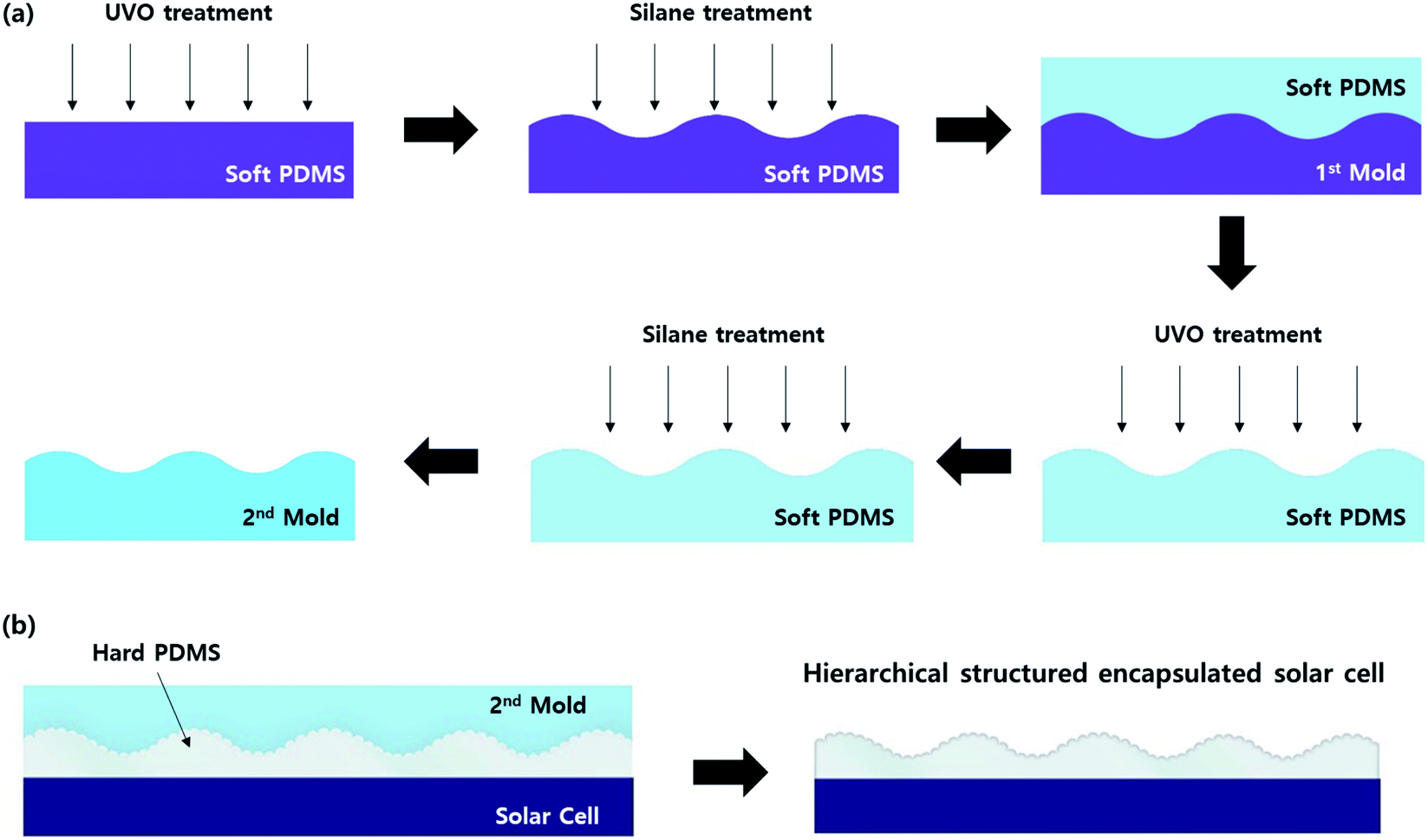 | ||
| Fig. 1 (a) Schematic of hierarchical structured mold fabrication process with ozone and silane treatment on polydimethylsiloxane (PDMS) surface and (b) encapsulation process of passivated emitter and rear cell (PERC) solar cell using mold. | ||
| Samples | Silane treatment (concentration (ml), time (h)) | |
|---|---|---|
| 1st mold | 2nd mold | |
| Struct. 1 | — | — |
| Struct. 2 | 0.4 ml, 5 h | 0.4 ml, 5 h |
| Struct. 3 | 0.4 ml, 5 h | 0.04 ml, 1 h |
| Struct. 4 | 0.04 ml, 1 h | 0.04 ml, 1 h |
| Struct. 5 | 0.4 ml, 5 h | — |
2.2 PDMS encapsulation of a Si solar cell
PERC (LWM5BB, Lightway) solar cells were encapsulated using a hard-PDMS (SR-580A and SR-580B, Heesung STS) casting process. A 1:1 (v/v) mixture of pre-polymer (SR-580A) and curing agent (SR-580B) were coated on a masked Si solar cell by bar coating method (No 2, RDS) for patternless structure (Structure 1), and the encapsulated hard-PDMS was cured in an oven for 1 hour at 70 °C.
The structured encapsulated Si solar cell were stamped mold on masked area with hard-PDMS and curing for 1 hour at 70 °C. After curing, the stamp was removed so that the solar cells were encapsulated with the patterned structure. Encapsulation process by stamping were shown in Fig. 1(b) by schematic.
2.3 Characterization
The surface and cross-section of all molds and encapsulated solar cells were evaluated by analyzing the images obtained using field-emission scanning electron microscopy (FE-SEM; S4800; Hitachi). The photovoltaic performance of the encapsulated solar cells was measured by first calibrating a solar simulator (Sun 2000, 1000 W Xenon source; Abet Technologies; 2400 Keithley source meter) with a KG-3 filter and an NREL-certified reference cell, and then setting the simulator to 1 sun, 1.5 AM conditions. The photovoltaic performance was measured with respect to the Angle of Incident (AOI) using a custom jig that was designed to accurately tilt the plane.Water-wetting angle measurements were conducted using a contact-angle system (Phoenix-300, SEO). Haze-effect images produced by red laser light were captured using a camera (Mightex, CCE-C013-U) that was focused using a lens (Azure-1214 mm). The light source was transmitted through the PDMS films and illuminated a white screen located 47 cm behind the PDMS film. The measurement was conducted in blackout conditions.
The incident photon to current conversion efficiency spectrum was measured using an Oriel (IQE-200TM, Newport Corp.) instrument equipped with a 250 W quartz tungsten halogen lamp light source, a monochromator, optical chopper, lock-in amplifier, and calibrated Si photodetector. The spectral response and intensity of the lamp were calibrated using a mono-Si detector.
3. Results and discussion
3.1 Hierarchical structure
Epidermis structures on leaf surfaces play several roles, such as super-hydrophobic self-cleaning, and guiding light into cylindrical palisade cells that contain a high concentration of chloroplasts for photosynthesis, as illustrated in Fig. 2(a).28 Leaf epidermis structure designs range from micrometer- to millimeter-scales depending on plant species and environment. As shown in Fig. 1(a), these structures can be applied to crystalline Si-based photovoltaic cells by encapsulation with silicone-based materials that are cast using molding or surface modification techniques. It would be highly challenging to create similar structures in EVA-glass encapsulating films.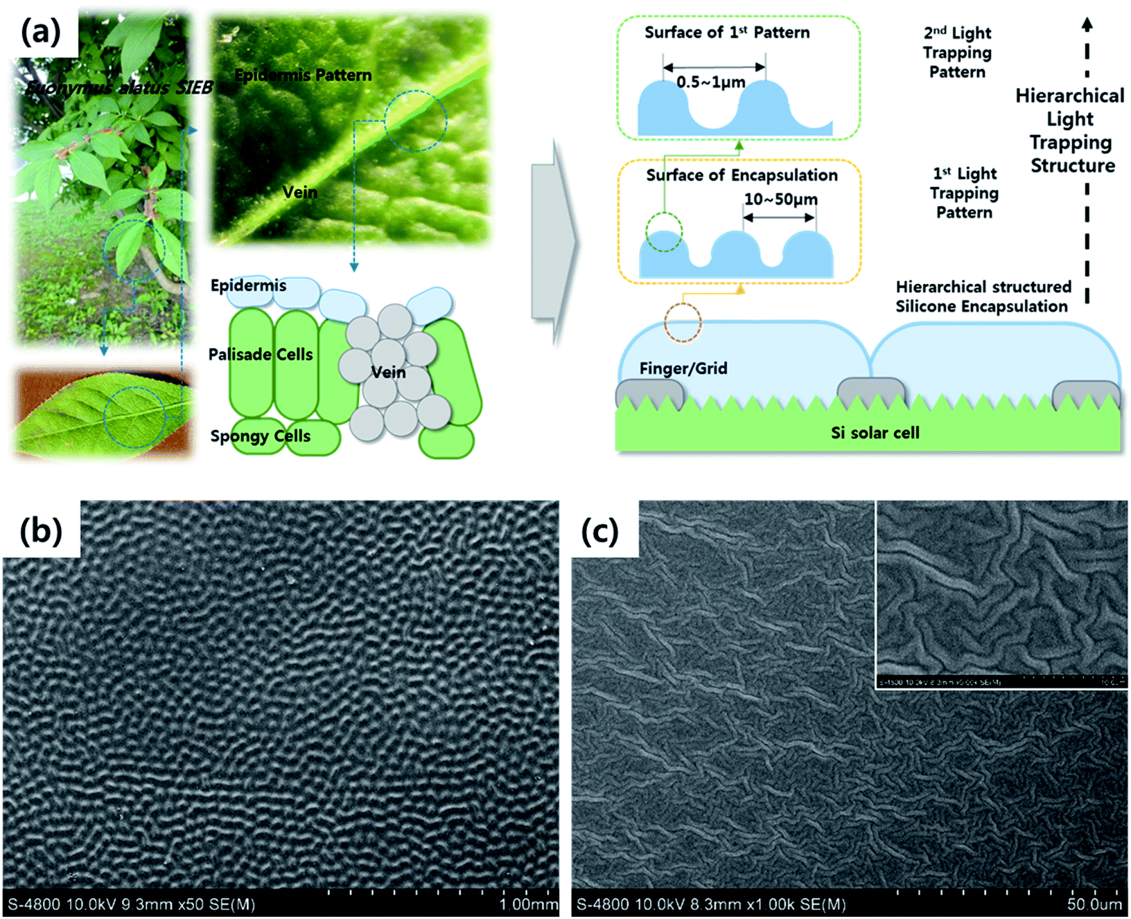 | ||
| Fig. 2 (a) Schematic of the concept of mimicking leaf epidermis structures for PDMS encapsulation of PERC solar cells using hierarchical structures. Scanning electron microscope (SEM) micrographs of PDMS film surfaces after (b) silane treatment with 0.4 ml of trichloro(1H,1H,2H,2H-perfluorooctyl) silane for 5 hours in vacuum and (c) ozone treatment for 10 minutes. | ||
This study used silane and ozone surface treatments to pattern silicone materials, as both methods are relatively simple to use for the fabrication of large-area homogeneous patterns. Polydimethylsiloxane (PDMS) was patterned by evaporating silane solution to generate tens-of-micrometer-scale patterns on the silicone surface according to treatment time and silane solution concentration, as shown in Fig. 2(b). By controlling the treatment parameters, several morphologies can be obtained. By high concentration and longer treatment time, first surface-bump are formed and then increased number of sharp bumps, after that continuous sharp bumps make hill-valley surface (Fig. S1†). Ozone treatment of PDMS results in sub-micrometer wave patterns that are a function of treatment time and ozone power as shown in Fig. 2(c) and S2.†29–31 From ozone treatment, sub-micrometer wave patterns are formed from the center of spiral. With the small amount of treatment time, the wave patterns start to form of a spiral and with increasing of treatment time, the wave patterns are clearly formed and meet with other wave patterns that are formed from other center of spiral. Then forgathered wave patterns are arranged finally. Both treatments create a thin layer of relatively stable silica on the PDMS surface, reliable silicone encapsulation process is possible with PDMS curing and peeling off from the other surface of PDMS. The patterns produced using each technique are of different length scales, so they can be combined into hierarchical structures.
Five surface structures were prepared by stamping a PDMS encapsulation layer on the surface of PERC solar cells using a PDMS stamp-during-curing process. The PDMS stamps included a combined or single pattern generated using silane and/or ozone treatment. The reference case, referred to as Structure 1, was fabricated using an unpatterned PDMS encapsulation layer. Structure 2 comprised large hill-valley and submicron wave patterns, as shown in Fig. 3(a). Similarly, Structure 3 comprised surface-bump and submicron wave patterns, as shown in Fig. 3(b). Structure 4 was fabricated using only wave patterns, as shown in Fig. 3(c), and Structure 5 only featured hill-valley patterns, as shown in Fig. 3(d). The micrographs show that the combined structures were well constructed on the PDMS surface to be used for the encapsulation of PERC solar cells, so that the structure mimicked leaf epidermises.
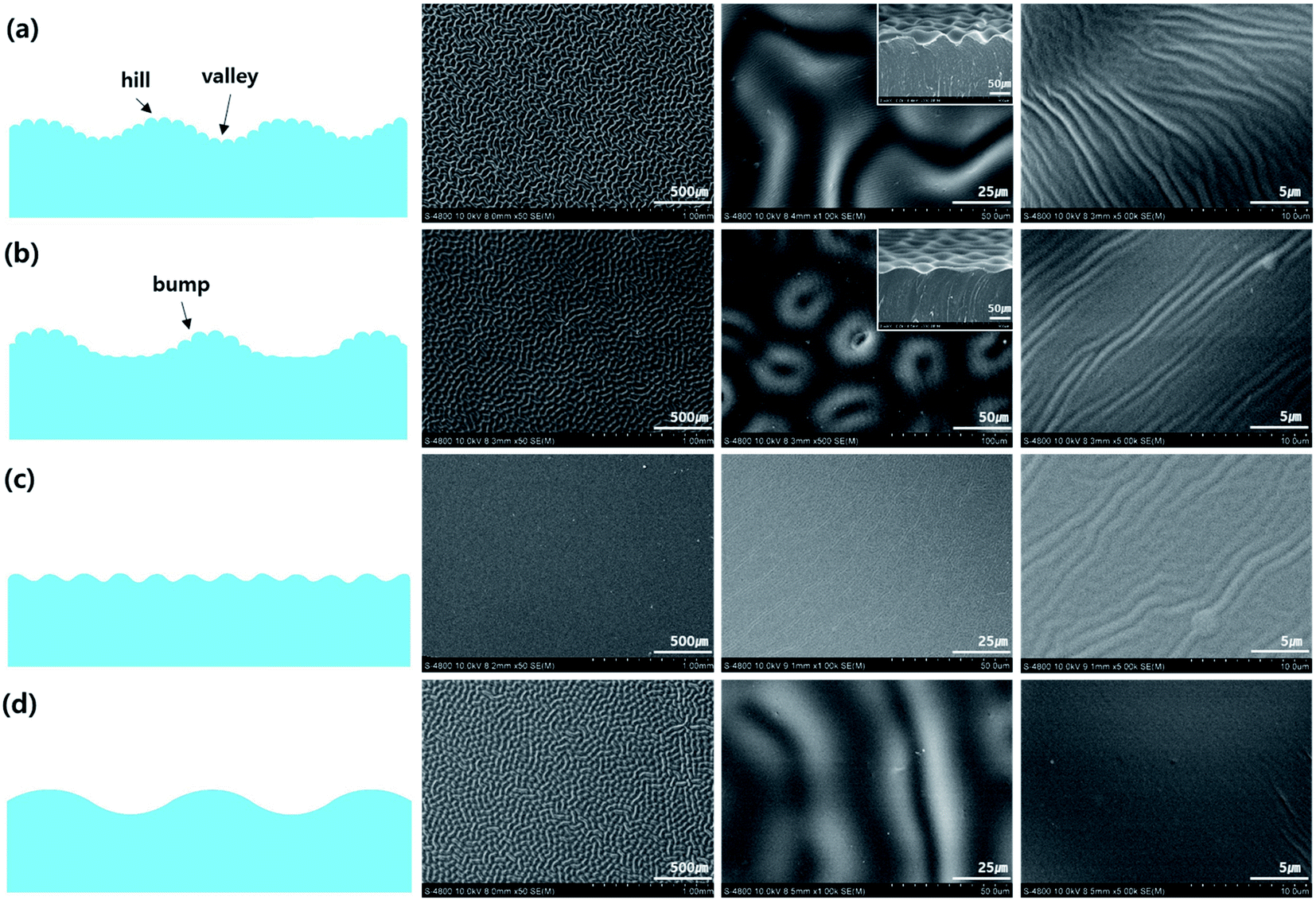 | ||
| Fig. 3 SEM images of PDMS surfaces with patterns created by a combination of silane and ozone treatment. (a) Hill-valley structures with submicron wave patterns (Structure 2), (b) surface-bump structures with submicron wave patterns (Structure 3), (c) submicron wave patterns (Structure 4), and (d) hill-valley structures without submicron patterns (Structure 5). | ||
3.2 Characteristic of hierarchical structured surface
The PDMS encapsulation patterns modified the beam path of incoming light and surface-wetting properties, as shown in Fig. 4. As shown in Fig. 4(a), the PDMS film surface structure altered light transmission behavior. The hill-valley structure with submicron wave patterns (Structure 2), and the pattern with only hill-valley structures (Structure 5), produced some light haze. Only the submicron wave pattern (Structure 4) enabled clear light transmission without haze. These effects can be expressed quantitatively by the parallel and diffuse transmission of each structured PDMS film, as shown in Fig. 4(b). The transmission of Structure 5 was 90.7%, whereas the transmission of each of the other films ranged from 94.5–95.5%. As is most clearly illustrated by Structure 5, the large-scale patterns induced backward scattering and decreased light transmission. However, Structure 4 shows that the submicron wave pattern did not have a notable effect. It is interesting to note that the combination of submicron wave patterns and large-scale patterns restored the light transmission, such that the total transmission of Structures 2 and 3 were similar to the untreated Structure 1. Therefore, the submicron wave pattern synergizes with the large-scale hill-valley or surface-bump patterns to improve transmission. The surface patterns further synergize with regard to haze effects. Structure 4 produced a similar degree of haze to the unpatterned reference structure, but Structures 2, 3, and 5 produced significant haze. These observations suggest that large-scale patterns produce haze, while submicron wave patterns do not. The amount of haze or diffused light differed according to the specific large-scale pattern, and the hill-valley structures appeared to create a stronger haze effect. Structures 2 and 5 used the same large-scale pattern, but featured different submicron wave patterns that resulted in a substantial difference in light diffusion. Therefore, it can be concluded that tens-of-micron or submicron patterns have a synergistic effect on light haze, and that submicron patterns play a significant role in hazing on a serrated surface. PDMS light diffusing patterns were estimated by measuring the intensity of transmitted laser light, as shown in Fig. 4(c). The similar patterns produced by Structures 3 and 5 indicate that large-scale patterns dictate scattering behavior, while Structure 4 produced a diffraction-like pattern, suggesting a synergistic effect between transmission and hazing.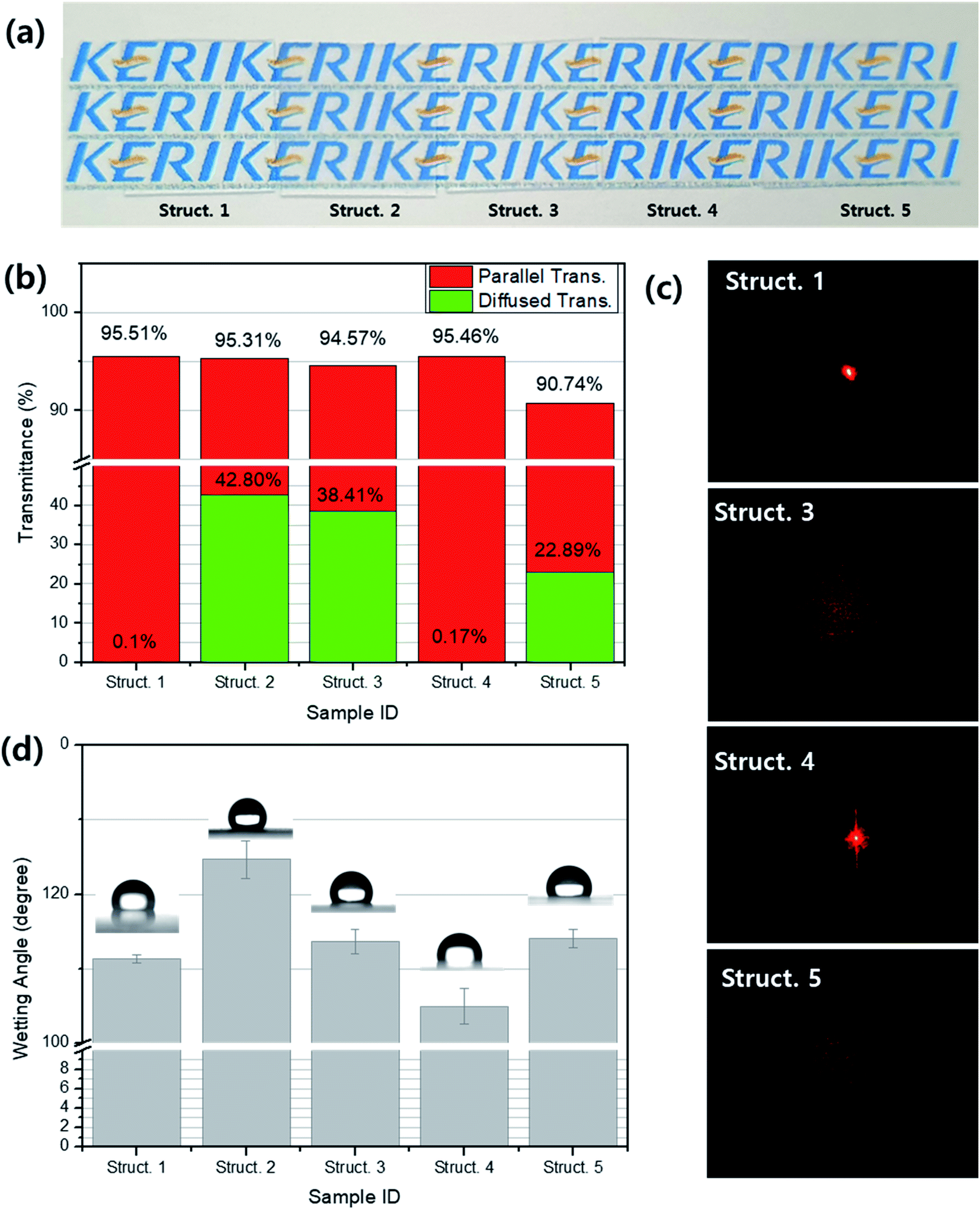 | ||
| Fig. 4 (a) Photographs of PDMS films with hierarchical or single patterns. (b) Haze measurement of each PDMS film with the indicated value of total and diffuse transmission. (c) Photographs of the red laser light after transmission through PDMS film patterns that arrived at a screen 47 cm behind the PDMS films. (d) The measured wetting angle of water droplets on the different PDMS films. | ||
The PDMS surface patterns do not only affect the capture of light, but also surface wetting capabilities, as shown in Fig. 4(d). Flat PDMS films were measured to have a wetting angle of 111°, which was decreased to 105° by the introduction of a submicron wave pattern. The large-scale hill-valley pattern (i.e., Structure 5) increased the wetting angle to 114°, and the combination of the two patterns that defined Structure 2 increased the wetting angle to 125°, as shown in Fig. 4(d). It is interesting to note that the hierarchical structures inspired by leaf epidermis structures, which comprised large-scale and submicron wave patterns, resulted in synergistic enhancement of haze, transmission, and surface wetting properties. This implies that encapsulation by silicone materials, with surfaces that can be modified chemically and geometrically using low-cost processes, has significant potential to improve the performance of crystalline Si-based solar cell modules, and further studies are required and expected in this field.
3.3 Performance of hierarchical structure encapsulated solar cell
Hierarchical patterns can be applied during crystalline Si-based solar cell module encapsulation using simple casting-based processes. Each structured PDMS surface patterns were printed using a PDMS mold on the surface of Si solar cell. Fig. 5(a) reveal modifications to haze, light transmission, and wetting properties, which are identical to the PDMS films with the hierarchical patterns. The performance of PERC solar cells encapsulated using patterned PDMS films under a vertically incident light source (1 sun, 1.5 air mass (AM) coefficient) are shown in Fig. 5(b), (c) and (d). Fig. 5(b) presents current density as a function of applied voltage, which reveals that unpatterned PDMS encapsulation improved the efficiency of solar cells when compared to bare cells. The different surface morphologies yielded some improvements, but these were not significant under vertical illumination. In contrast, conventional encapsulation using an EVA-glass layer on a bare cell reduced efficiency.16–19 Whereas EVA-glass layers absorbed short-wavelength radiation, the PDMS layer allowed transmission of the wider spectrum, as shown in Fig. 5(e). Additionally, light scattered and reflected by the PERC cell surface can reportedly be captured by internal reflection from the PDMS layer.21,27 The combination of these effects results in an improved efficiency of the PDMS-encapsulated solar cell. Considering that conventional encapsulation of solar cells reduces their efficiency, PDMS encapsulation provides clear benefits as a substitute for EVA-glass. Furthermore PDMS is not affected by radiation browning, can be fabricated with a hydrophobic surface, and is easier to form into more complex designs.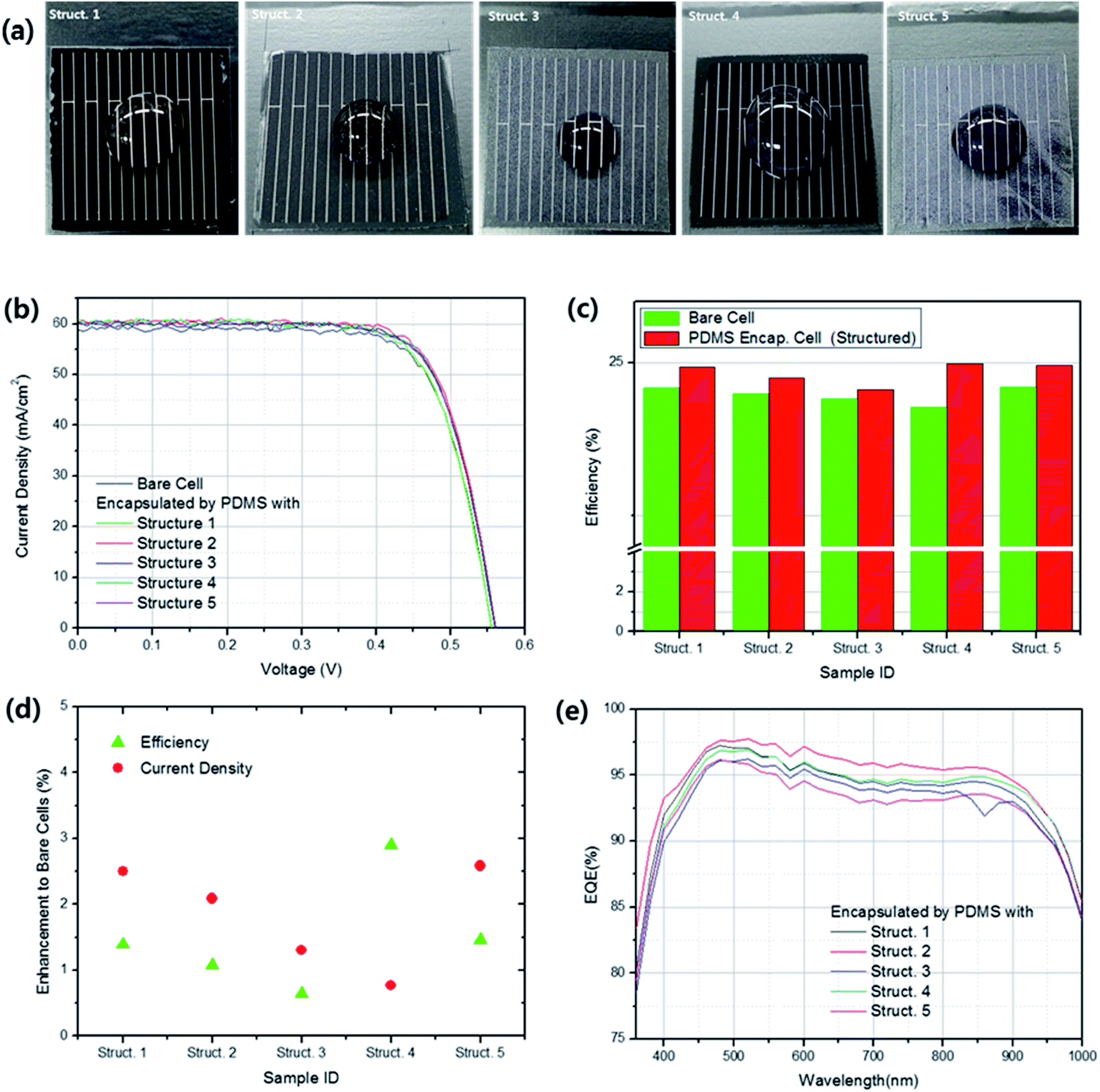 | ||
| Fig. 5 (a) Photographs of the PDMS-encapsulated PERC cells with a single water droplet. (b) The relationship between current density and applied voltage (I–V curve) of PDMS-encapsulated PERC cells with different surface structures and bare PERC cells. (c) The efficiency of the PERC solar cells before and after PDMS-encapsulation under vertical illumination (1 sun, 1.5 AM). (d) The efficiency and current density enhancement of bare cells by PDMS-encapsulation with different patterns. (e) Incident photon to current density efficiency (IPCE) of PDMS-encapsulated PERC solar cells. | ||
When exposed to vertical light, submicron wave patterns yielded greater efficiency enhancement than hierarchical structures, as shown in Fig. 5(c) and (d). This implies that the hazing of incident light is not beneficial to energy conversion under vertical illumination. Furthermore, the higher current density of Structures 4 and 5 does not guarantee an increase in efficiency due to open circuit voltage and fill-factor effects, as listed in Table 2. Considering the increasing value of current density of structure 2 and structure 5, hill-valley structure could play a micro-lens on the solar cell for focusing the incident light. In case of structure 2 that has hill-valley structure same shows little lower than structure 5 because that submicron wave patterns scatter the incident light. Relating with our assumption it needs analysis further with theoretical consideration.
| Samples | Bare cell | PDMS encapsulated | ||||||
|---|---|---|---|---|---|---|---|---|
| Jsc (mA cm−2) | Voc (V) | Fill factor | Efficiency (%) | Jsc (mA cm−2) | Voc (V) | Fill factor | Efficiency (%) | |
| Struct. 1 | 58.895 | 0.559 | 0.747 | 24.587 | 60.367 | 0.557 | 0.741 | 24.929 |
| Struct. 2 | 59.467 | 0.556 | 0.740 | 24.485 | 60.710 | 0.556 | 0.733 | 24.749 |
| Struct. 3 | 59.604 | 0.555 | 0.738 | 24.403 | 60.381 | 0.554 | 0.734 | 24.561 |
| Struct. 4 | 59.971 | 0.550 | 0.736 | 24.273 | 60.434 | 0.556 | 0.742 | 24.977 |
| Struct. 5 | 59.985 | 0.557 | 0.730 | 24.383 | 61.163 | 0.556 | 0.731 | 24.870 |
The effects of hierarchical surface patterns are most notable when PDMS-encapsulated devices are illuminated at oblique angles, as shown in Fig. 6(a) and (b) (see ESI Fig. S3 and S4† for efficiency and current density variation as a function of AOI for all surface patterns tested). The efficiency of the bare PERC cell decreased as the AOI was increased, as shown in Fig. 6(a) and (b).32–34 Similarly, the efficiency of the unpatterned PDMS-encapsulated sample also decreased, but maintained a higher efficiency than the bare sample at all AOIs. The difference in conversion efficiency between the bare cell and Structure 2 increased as a function of AOI, demonstrating that the encapsulated device performed significantly better for a high AOI. Of all structures fabricated for this study, the PDMS-encapsulated devices had an enhanced efficiency for all AOI measured, as shown in Fig. 6(c). However, the amount of enhancement differed according to the PDMS surface structure. The conversion efficiency of the unpatterned PDMS sample was greater than that of the bare PERC cell until the AOI exceeded 50°. The conversion efficiency of Structure 2 increased up to a 60° AOI, where the enhancement was 7%. The hill-valley surface of Structure 5 has an increased conversion efficiency up to a 40° AOI, with a similar enhancement to Structure 2. From these results, introducing submicron wave patterns on the surface enhances solar cell performance at high AOI. However, submicron wave patterns alone did not increase conversion efficiency for large AOIs. These results indicate that the improved omni-directional light capture by hierarchical structures is a result of the synergistic effects of different patterns with sub- and tens-of-micrometer length scales. Fig. 6(d) presents the expected total electricity production of each PDMS surface pattern. Assuming that all incident light has the same 1 sun intensity, the most energy was produced by the hierarchical PDMS-encapsulated structure due to its excellent omni-direction light-capture behavior. If obliquely incident light has a weaker intensity that follows the cosine law, the submicron wave pattern would produce the greatest energy due to its superior performance under vertically incident light. Therefore, pattern structures should be selected according to expected use.
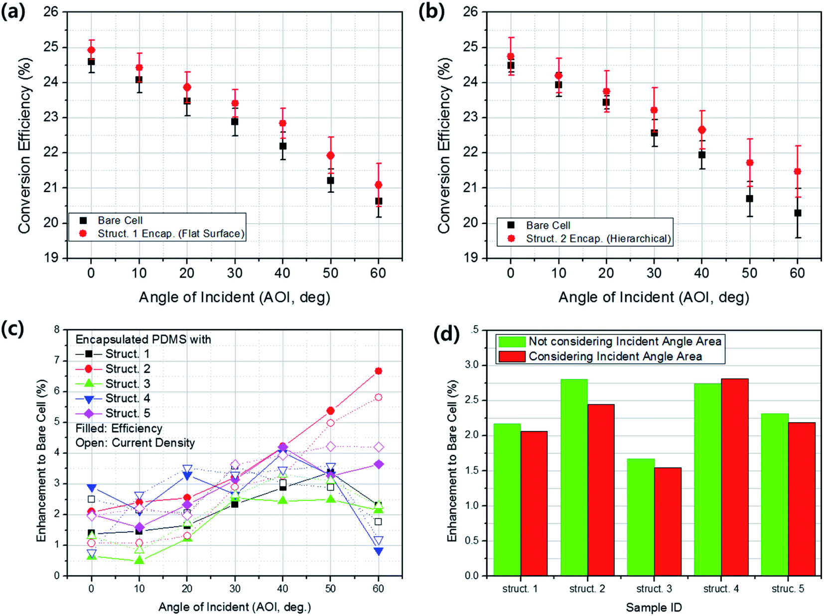 | ||
| Fig. 6 Energy conversion efficiency according to the angle of incidence (AOI) for (a) unpatterned PDMS and (b) hierarchical structures with hill-valley and submicron wave. (c) Efficiency enhancement and current density of bare cells and PDMS-encapsulated cells with various surface patterns and (d) the expected energy production enhancement of each structure. | ||
The silicone-encapsulation of crystalline Si-based solar cells has many obvious benefits when compared to conventional EVA-glass encapsulation. This study demonstrated an additional advantage of silicone-based encapsulation, specifically surface modifications that improve light-trapping and hydrophobicity. Hierarchical patterns inspired by leaf epidermis structures comprising tens-of-micrometer and submicron patterns were fabricated on PDMS surfaces, using low-cost silane and ozone treatments, for the encapsulation of PERC solar cells. These bio-inspired structures have an increased wetting angle of 125° and improved solar cell performance at all AOI due to omni-direction light capture. However, further studies should be conducted to better optimize the structures from theoretical and process perspectives.
4. Conclusion
Photovoltaic modules based on crystalline Si solar cells require innovation, and silicone-based encapsulation methods are considered to be a promising improvement over conventional EVA-glass-based encapsulation. The use of silicone materials such as PDMS allows the surface of the photovoltaic module to be easily modified so that light can be better captured, and hydrophobicity can be increased. Hierarchical patterns inspired by leaf epidermis structures were applied to PDMS prior to the encapsulation of PERC solar cells. The patterns comprised tens-of-micrometer and submicron patterns produced using ozone and hill-valley or surface-bump morphologies produced using silane treatment, respectively. The synergistic effects of the combination two type of patterns length scales improved light transmission, haze, and wetting angle to an extent that cannot be achieved with a single pattern. Furthermore, the photovoltaic performance of cells encapsulated by these hierarchical patterns exhibited synergistic efficiency improvements when exposed to vertical and oblique light, resulting in omni-directional electricity production enhancement. Considering the efficiency losses when EVA-glass encapsulation is used, we suggest that PDMS encapsulation with easily fabricated hierarchical structures presents new possibilities for advanced photovoltaic module developments. More efficient structures and cost-effective processes should be researched further.Conflicts of interest
There are no conflicts of interests to declare.Acknowledgements
This research was supported by the Korea Electrotechnology Research Institute (KERI) Primary Research Program through the National Research Council of Science & Technology (NST) funded by the Ministry of Science and ICT (MSIT) (No. 19-12-N0101-28).References
- C. Battaglia, A. Cuevas and S. De Wolf, High-efficiency crystalline silicon solar cells: status and perspective, Energy & Environmental Science, 2016, 9, 1552–1576 Search PubMed.
- M. A. Green, The Passivated Emitter and Rear Cell (PERC): From conception to mass production, Sol. Energy Mater. Sol. Cells, 2015, 143, 190–197 CrossRef CAS.
- E. Schneiderlochner, R. Preu, R. Ludemann and W. W. Glunz, Laser-fired rear contacts for crystalline solar cells, Progress in Photovoltaics: Research and Applications, 2002, 10, 29–34 CrossRef CAS.
- H. Hieslmair, J. Appel, J. Kassthuri, J. Guo, B. Johnson and J. Binns, Impact of the injection-level-dependent lifetime on Voc, FF, ideality m, J02, and the dim light response in a commercial PERC cell, Progress in Photovoltaics: Research and Applications, 2016, 24, 1448–1457 CrossRef CAS.
- F. Schindler, S. Schon, B. Michl, S. Riepe, P. Krenckel, J. Benick, F. Feldmann, M. Hermle, S. W. Glunz, W. Warta and M. C. Schubert, High-efficiency multicrystalline silicon solar cells: potential of n-type doping, IEEE Journal of Photovoltaics, 2015, 5, 1571–1579 Search PubMed.
- J. Benick, A. Richter, R. Muller, H. Hauser, F. Feldmann, P. Krenckel, S. Riepe, F. Schindler, M. C. Schubert, M. Hermle, A. W. Bett and S. W. Glunz, High-efficiency n-type HP mc silicon solar cells, IEEE Journal of Photovoltaics, 2017, 7, 1171–1175 Search PubMed.
- A. Richter, J. Benick, F. Feldmann, A. Fell and M. Bermle, n-type Si solar cells with passivating electron contact: identifying sources for efficiency limitations by wafer thickness and resistivity variation, Sol. Energy Mater. Sol. Cells, 2017, 173, 96–105 CrossRef CAS.
- C. Yu, S. Xu, J. Yao and S. Han, Recent advances in and new perspectives on crystalline silicon solar cells with carrier-selective passivation contacts, Crystals, 2018, 8, 430 CrossRef.
- E. Franklin, K. Fong, K. McIntosh, A. Fell, A. Blakers, T. Kho, D. Walter, D. Wang, N. Zin, M. Stokes, E.-C. Wang, N. Grant, Y. Wan, Y. Yang, X. Zhang, Z. Feng and P. J. Verlinden, Design, fabrication and characterization of a 24.4% efficient interdigitated back contact solar cell, Progress in Photovoltaics: Research and Applications, 2016, 24, 411–427 CrossRef CAS.
- M. Hermie, F. Granek, O. Schultz and S. W. Glunz, Analyzing the effects of front-surface fields on back-junction silicon solar cells using the charge-collection probability and the reciprocity theorem, J. Appl. Phys., 2008, 103, 054507 CrossRef.
- M. K. Mat Desa, S. Sapeai, A. W. Azhari, K. Sopian, M. Y. Sulaimanm, N. Amin and S. H. Zaidi, Silicon back contact solar cell configuration: a pathway towards higher efficiency, Renewable Sustainable Energy Rev., 2016, 60, 1516–1532 CrossRef CAS.
- S. M. Kim, S. Chun, M. G. Kang, H.-E. Song, J.-H. Lee, H. Boo, S. Bae, Y. Kang, H.-S. Lee and D. Kim, Simulation of interdigitated back contact solar cell with trench structure, J. Appl. Phys., 2015, 117, 074503 CrossRef.
- K. Yoshikawa, H. Kawasaki, W. Yoshida, T. Irie, K. Konish, K. Nakano, T. Uto, D. Adachi, M. Kanematsu, H. Uzu and K. Yamamoto, Silicon heterojunction solar cell with interdigitated back contact for a photoconversion efficiency over 26%, Nat. Energy, 2017, 2, 17032 CrossRef CAS.
- M. Tan, S. Zhong, W. Wang and W. Shen, Silicon homo-heterojunction solar cells: a promising candidate to realize high performance more stably, AIP Adv., 2017, 7, 085016 CrossRef.
- M. Taguchi, A. Yano, S. Tohoda, K. Matsuyama, Y. Nakamura, T. Nishiwaki, K. Fujita and E. Maruyama, 24.7% Record efficiency HIT solar cell on thin silicon wafer, IEEE Journal of Photovoltaics, 2014, 4, 96–99 Search PubMed.
- W. H. Holley, S. C. Agro, J. P. Gailca, L. A. Thoma and R. S. Yorgensen, Investigation into the causes of browning in EVA encapsulated flat panel PV modules, Proceedings of 1994 IEEE 1st World Conference on Photovoltaic Energy Conversion, 1994, pp. 894–896 Search PubMed.
- M. Kontges et al., Assessment of photovoltaic module failures in the field, Photovoltaic Power System Programme, Report IEA-PVPS T13-09, 2017 Search PubMed.
- M. R. Vogt, et al., Optical constants of UV transparent EVA and the impact on the PV module output power under realistic irradiation, Energy Procedia, 2016, 92, 523–530 CrossRef CAS.
- B. Paviet-Salomon, et al., Back-contacted silicon heterojunction solar cells: optical-loss analysis and mitigation, IEEE Journal of Photovoltaics, 2015, 5, 1293–1303 Search PubMed.
- T. S. Liang, et al., A review of crystalline silicon bifacial photovoltaic performance characterization and simulation, Energy Environ. Sci., 2019, 12, 116–148 RSC.
- F.-H. Chen, S. Pathreeker, J. Kaur and I. D. Hosein, Increasing light capture in silicon solar cells with encapsulants incorporating air prisms to reduce metallic contact losses, Opt. Express, 2016, 24, A1419 CrossRef CAS.
- J. Govaerts, et al., Developing an advanced module for back-contact solar cells, IEEE Trans. Compon., Packag., Manuf. Technol., 2011, 1, 1319–1327 CAS.
- C. Peike, I. Hadrich, K.-A. Weiß and I. Durr, Overview of PV module encapsulation materials, Photovolt. Int., 2013, 19, 85–92 Search PubMed.
- S. Ohl and G. Hahn, Increased internal quantum efficiency of encapsulated solar cells by using two-component silicone as encapsulation material, 23rd European Photovoltaic Solar Energy Conference and Exhibition, Valencia, Spain, 2008, pp. 2693–2697 Search PubMed.
- B. Ketola, K. R. McIntosh, A. Norris and M. K. Tomalia, Silicones for Photovoltaic Encapsulation, 23rd European Photovoltaic Solar Energy Conference and Exhibition, Valencia, Spain, 2008, pp. 2969–2973 Search PubMed.
- K. R. McIntosh, J. N. Cotsell, A. W. Norris, N. E. Powell and B. M. Ketola, An optical comparison of silicone and EVA encapsulants under various spectra, 35th IEEE Photovoltaic Specialists Conference, Honolulu, USA, 2010 Search PubMed.
- M. J. Yun, Y. H. Sim, S. I. Cha and D. Y. Lee, Finding 10% hidden electricity in crystalline Si solar cells using PDMS coating and three-dimensional cell arrays, Progress in Photovoltaics: Research and Applications, 2020, 28, 372–381 CrossRef CAS.
- J. H. McClendon, The micro-optics of leaves. I. Patterns of reflection from the epidermis, Am. J. Bot., 1984, 71, 1391–1397 CrossRef.
- Y.-J. Fu, et al., Effect of UV-ozone treatment on poly(dimethylsiloxane) membranes: surface characterization and gas separation performance, Langmuir, 2010, 26, 4392–4399 CrossRef CAS.
- Y. Berdichevsky, J. Khadurina, A. Guttman and Y.-H. Lo, UV/Ozone modification of poly (dimethylsiloxane) microfluidic channels, Sens. Actuators, B, 2004, 97, 402–408 CrossRef CAS.
- K. Ma, J. Rivera, G. J. Hirasaki and S. L. Biswal, Wettability control and patterning of PDMS using UV-ozone and water immersion, J. Colloid Interface Sci., 2011, 363, 371–378 CrossRef CAS.
- J. L. Balenzategui and F. Chenlo, Measurement and analysis of angular response of bare and encapsulated silicon solar cells, Sol. Energy Mater. Sol. Cells, 2005, 86, 53–83 CrossRef CAS.
- F. Plag, I. Kroger, T. Fey, F. Witt and S. Winter, Angular-dependent spectral responsivity: traceable measurements on optical losses in PV devices, Progress in Photovoltaics: Research and Applications, 2017, 25, 1–14 CrossRef.
- A. Louwen, A. C. de Waal, R. E. I. Schropp, A. P. C. Faaji and W. G. J. H. M. van Sark, Comprehensive characterization and analysis of PV module performance under real operation conditions, Progress in Photovoltaics: Research and Applications, 2017, 25, 218–232 CrossRef.
Footnote |
| † Electronic supplementary information (ESI) available. See DOI: 10.1039/d0ra03378b |
| This journal is © The Royal Society of Chemistry 2020 |