
 Open Access Article
 This Open Access Article is licensed under a Creative Commons Attribution-Non Commercial 3.0 Unported Licence
Arrayed nanopore silver thin films for surface-enhanced Raman scattering†
Weiwei Zhang ab,
Qingkun Tiana,
Zhanghua Chena,
Cuicui Zhaoa,
Haishuai Chaia,
Qiong Wua,
Wengang Lic,
Xinhua Chend,
Yida Deng*e and
Yujun Song*a
ab,
Qingkun Tiana,
Zhanghua Chena,
Cuicui Zhaoa,
Haishuai Chaia,
Qiong Wua,
Wengang Lic,
Xinhua Chend,
Yida Deng*e and
Yujun Song*a
aCentre for Modern Physics Technology, School of Mathematics and Physics, University of Science and Technology, Beijing, Xueyuan Road 30, Haidian District, Beijing, 100083, China. E-mail: songyj@ustb.edu.cn
bShunde Graduate School of University of Science and Technology Beijing, Daliang Zhihui Road 2, Shunde Distinct, Foshan, 528399, China
cXiangan Affiliated Hospital, Xiamen University, Siming North Road 422, Siming District, Xiamen, Fujian 361005, China
dDepartment of Hepatobiliary and Pancreatic Surgery, The First Affiliated Hospital, School of Medicine, Key Laboratory of Combined Multi-organ Transplantation, Ministry of Public Health, Zhejiang University, Hangzhou 310003, China
eTianjin Key Laboratory of Composite and Functional Materials, School of Materials Science and Engineering, Tianjin University, Weijin Road 92, Nankai District, Tianjin, 300350, China. E-mail: yida.deng@tju.edu.cn
First published on 23rd June 2020
Abstract
Active substrates are crucial for surface-enhanced Raman scattering (SERS). Among these substrates, large uniform area arrayed nanoporous silver thin films have been developed as active substrates. Arrayed nanoporous silver thin films with unique anisotropic morphologies and nanoporous structures can be fabricated onto the nanoporous anodic aluminum oxide (AAO) of controlled pore size and interspacing by precisely tuning the sputtering parameters. These thin films preserve locally enhanced electromagnetic fields by exciting the surface plasmon resonance, which is beneficial for SERS. In this study, nanoporous silver thin films were transferred into polymethylmethacrylate (PMMA) and polydimethylsiloxane (PDMS) substrates using our recently invented template-assisted sol–gel phase inverse-imprinting process to form two different nanopore thin films. The as-formed Ag nanoporous thin films on PMMA and PDMS exhibited intensively enhanced SERS signals using Rhodamine 6G (R6G) as the model molecule. The two nanopore thin films exhibited opposite pore size-dependent SERS tendencies, which were elucidated by the different enhancement tendencies of the electric field around pores of different diameters. In particular, the Ag nanoporous thin film on PMMA exhibited an R6G detection limit of as low as 10−6 mol L−1, and the SERS enhancement factor (EF) was more than 106. The low detection limit and large EF demonstrated the high sensitivity of the as-prepared SERS substrates for label-free detection of biomolecules. Compared with conventional smooth films, this nanopore structure can facilitate future application in biomolecular sensors, which allows the detection of single molecules via an electronic readout without requirement for amplification or labels.
Introduction
Surface-enhanced Raman scattering (SERS) facilitates ultra-sensitive high-resolution with a unique narrow band fingerprint, spectral specificity, non-destructive nature, and qualitative and quantitative analysis of a low detection module. To date, SERS technology, as a low-concentration detection method has been widely used in protein phosphorylation,1 exosomes from plasma of cancer patients,2 dyes,3–5 deoxyribonucleic acid (DNA)6,7 and ribonucleic acid (RNA)8–10 bases, secretion of cytokine (vascular endothelial growth factor),11 chemical and biological sensing,12 and oil/water mixture.13 SERS can amplify the original Raman signal by up to several orders of magnitude or more, leading to a dramatic increase in sensitivity and selectivity, and rapid response of signals.8–10,14The excitation of the surface plasmon resonance, which is an electromagnetic oscillation formed by the interaction between free electrons and incident photons in the near-field region of a metal surface is an important method to enhance Raman scattering. In plasmonic nanostructures (e.g., rods, dots, and nanopores), the interaction between metallic nanostructure materials (Pt, Au, Ag, Cu, Al, etc.) and light generates a strong electromagnetic field enhancement (or hot spots), which largely depends on the size, morphology, structural parameters, and metal types of the nanostructures.15,16 Recently, numerous efforts have been committed to the design of metallic SERS nanostructures, which mainly include metal nanoparticles and composite structures formed by metallic nanoparticles assembled on different template substrates.17–23 Some alternative approaches have also been invented such as the influence of morphology and material types on the substrates, to create substrates with strong and reproducible SERS signals using the lithographic process.24–27 These methods not only provide controllable periodicity of the nanostructures but also regulate the electromagnetic field enhancement.28
Among these structures, nanogaps29–32 and nanopores33,34 have been widely investigated owing to their ability to confine the electromagnetic field.35 In particular, nanopore arrays have been used in DNA sequencing technology, and hard (inorganic) nanopores present some advantages over soft biological or polymeric pores, such as robustness, thermal/mechanical/chemical versatility, and potential for device integration in wafer-scale integrated circuits.36–38 Although many lithography methods (e.g., electron beam lithography, nanosphere lithography, or soft lithography) can provide these advantages, they suffer from limitations, including a high cost and/or difficulties in obtaining large-area nano-patterned surfaces for commercial applications. Recently, anodic aluminum oxide (AAO) lithography can be used to fabricate large-area and cost-effective SERS substrates.39–41 Additionally, for the preparation of polycrystalline films, the magnetron sputtering deposition method has been used owing to its simplicity, low cost, high production speed, and scalability. Moreover, the magnetron sputtering process has distinct advantages (such as good adhesion to the substrate, uniformity of film thickness, and good control ability of the multi-layered interfaces during the deposition process) for large-scale production.42–45 Compared to gold and other reactive metallic nanomaterials,46,47 silver nanomaterials are preferred for many SERS applications, showing excellent performance for optical absorption, scattering signatures, and superior surface plasmon resonance that depends strongly on their surface morphologies, and surface electronic or dielectric properties, and interaction with substrates.48,49 However, most conventional substrates for SERS are based on a silicon wafer, glass wafer, and porous alumina, which have more drawbacks than a universal SERS substrate because of their rigid and brittle nature. Thus, these substrates are only applied to planar objects, and their signals are considerably influenced by the background interference, leading to a low signal to noise (S/N) ratio. Until now, a few polymers (such as a low-cost polymer casting of polydimethylsiloxane (PDMS) and polymethylmethacrylate (PMMA)) preserving the considerably low background interference embedded with metallic nanostructures have been developed as active SERS substrates.50–56 As a supporting substrate, PMMA and PDMS possess outstanding optical transparency (92% for PMMA and 83% for PDMS), and a laser can easily pass through and reach the probing molecule layer, enhancing the S/N ratio.
Rhodamine 6G (R6G) is one of the Rhodamine family dyes. It has a Raman cross-section on the order of 10−22 cm2, and it is often used as a standard probing molecule for the sensitivity calibration of SERS effects, nonlinear vibrational detection, UV-Vis-NIR sum-frequency generation, and nanometer-scale detection using near-field Raman spectroscopy. Eqn (1)57,58 provides an estimation of the SERS enhancement factor (EF), where ISERS and INR represent the intensities of the SERS spectrum and Raman scattering spectra for R6G, respectively. NSERS and NNR represent the number of R6G molecules in the laser excitation area adsorbed on the composite film and in the bulk form, respectively.
 | (1) |
In this study, we aimed at preparing universal, transparent substrates with good mechanical properties and highly active SERS by developing a simple and low-cost method that can preserve large-scale production and good nanostructure controllability. A variety of anodic AAO templates with different apertures were first fabricated using the conventional two-step anodization process. Next, different thicknesses of silver layers were deposited on AAO templates via the magnetron sputtering method. Then, the prepared nanoporous thin films were embedded into the PMMA and PDMS substrates using the invented template-assisted sol–gel inverse-imprinting process. Finally, an active SERS molecule with a silver layer embedded onto the PMMA and PDMS substrates was obtained. We experimentally and theoretically demonstrated that the EF factor of SERS can be distinctly increased owing to the considerably enhanced electromagnetic field.
In this study, a novel nanoporous SERS probe was prototyped for detection of R6G at a low concentration by low-cost polymer casting of PDMS and PMMA and nanoporous films of varying sizes and shapes. Compared with other substrates, the localized surface plasmon resonance can be flexibly tuned by controlling the diameter, interspacing, and Ag thickness. The sensors with soft PDMS substrate can be potentially used in wearable devices. Moreover, this nanopore structure exhibits potential in biomolecular sensors, which allows the detection of single molecules via an electronic readout without requirement for amplification or labels.
Results and discussion
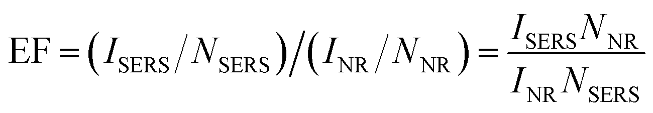
Fig. 1a–c show SEM images of the nanoporous silver films with a thickness of 90 nm that were deposited on the AAO/Al templates with pristine AAO diameters of 50 nm, 70 nm, and 90 nm respectively. As shown in these images, these thin films were formed by Ag atoms with slight accumulation around the holes, leading to the shrinkage of the pore diameters compared with the diameters of the pure AAO template. Moreover, the special inverted trapezoidal wall of the AAO templates resulted in the reduction of the pore diameter and deposition of Ag particles around the top of the inner walls.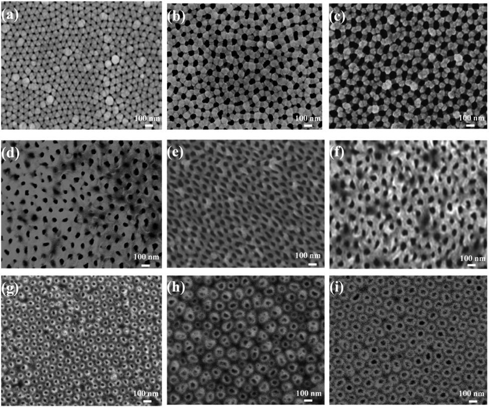 | ||
| Fig. 1 SEM images of the nanoporous silver films with different pore sizes based on the AAO templates. The thickness of the silver film was 90 nm, and the pristine AAO pore diameters were (a) 50, (b) 70, and (c) 90 nm. SEM characterization of the nanoporous silver films based on PMMA substrates was assisted by the different pore diameters. The thickness of the silver film was 90 nm, and the pristine AAO pore diameters were (d) 50, (e) 70, and (f) 90 nm. SEM characterization of the nanoporous silver films based on PDMS substrates was assisted by the different pore diameters. The thickness of the silver film was 90 nm, and the pristine AAO pore diameters were (g) 50, (h) 70, and (i) 90 nm. | ||
SEM images of the nanoporous Ag films attached to the PMMA (nanoporous Ag film/PMMA) and PDMS (nanoporous Ag film/PDMS) substrates are shown in Fig. 1d–f and g–i, respectively. Compared with the planar pore structure in Fig. 1d–f, there was a cylindrical-like structure on the top, as shown in Fig. 1g–i. This was because, in the AAO/Al removal process, the softer PDMS substrate could relieve much more stress in the nanopore films than the harder PMMA substrate, leading to a complete nanostructure. Thus, we can obtain two kinds of nanoporous silver films that could exhibit different electrical field distribution tendencies that depended on the pore size.
Fig. S1a in ESI† shows the absorption spectra of the nanoporous silver films on the PMMA templates. The spectra show different surface plasmon peak positions, resonance intensities, and peak widths, depending on their pore sizes. The samples have absorption peaks at approximately 340 nm, 583 nm, and 820 nm owing to plasmon resonance. The increase in the absorption intensity starting from 705 nm was because of PMMA, which is further confirmed in Fig. S1b.† The relative absorption intensity decreased with an increase in pore size. This was due to the fact that the increase in the pore size decreases the interaction area between the Ag and the light but increases the interaction area between the light and PMMA, which can allow more energy to pass through the PMMA membrane.
Fig. 2a–d show the SERS spectra of the R6G molecules adsorbed on the Ag film. As shown in these spectra, there is no distinct Raman band assigned to PMMA and PDMS according to the literature.59–63 We attribute this observation to the presence of substrate PMMA and PDMS at the deep bottom of the sample, covered by R6G molecules, thereby showing no distinct peak in the Raman spectra. Raman scattering peaks at 614 cm−1 and 640 cm−1 are from the C–C–C ring in-plane band. The peak at 774 cm−1 is induced by the out-of-plane bending motion of the hydrogen atoms in the xanthene skeleton. Peaks at 1129 cm−1 and 1187 cm−1 are ascribed to the C–H in-plane band, and the peak at 1574 cm−1 is assigned to the C![[double bond, length as m-dash]](https://www.rsc.org/images/entities/char_e001.gif) O stretching vibrations. The peaks at 1364 cm−1, 1599 cm−1, and 1651 cm−1 are bands owing to the C–C aromatic stretching vibrations.64–67 Here, the most prominent peak position at 614 cm−1 was used to calculate the EF values.
O stretching vibrations. The peaks at 1364 cm−1, 1599 cm−1, and 1651 cm−1 are bands owing to the C–C aromatic stretching vibrations.64–67 Here, the most prominent peak position at 614 cm−1 was used to calculate the EF values.
 | ||
| Fig. 2 (a) SERS of R6G absorbed on 90 nm-thick Ag nanoporous films deposited on the AAO templates with diameters of (i) 50, (ii) 70, and (iii) 90 nm; (b) SERS of R6G absorbed on (i) 50, (ii) 90, and (iii) 135 nm-thick Ag nanoporous films deposited on the same AAO template with a diameter of 90 nm; (c) SERS of R6G absorbed on 90 nm-thick Ag films transferred from AAO templates that had diameters of (i) 50, (ii) 70, and (iii) 90 nm to PMMA substrates; (d) SERS of R6G absorbed on (i) 50, (ii) 90, and (iii) 135 nm-thick Ag nanoporous films transferred from the same AAO template with a diameter of 90 nm to the PMMA substrates; (e) SERS of R6G absorbed on 90 nm-thick Ag films transferred from AAO templates with diameters of (i) 50, (ii) 70, and (iii) 90 nm to PMMA substrates. Curves (iv) in (a)–(d) show the SERS signal of R6G/PMMA with a concentration of 10−2 mol L−1. Curve (iv) in (e) shows the SERS signal of R6G/PDMS with a concentration of 10−2 mol L−1. | ||
In Fig. 2a, the intensity decreases with an increase in pore size. Fig. 2b shows the Ag thickness-dependent SERS of R6G on Ag/AAO samples fabricated on the AAO templates with a pore diameter of 90 nm. The SERS signal can be increased considerably as the Ag film thickness is increased from 50 nm to 135 nm. These results arise from destructive interference effects induced by the pore size and Ag thickness in the presence of the Al film, which has been experimental confirmed previously.68
Fig. 2c and d show SERS spectra of R6G adsorbed on nanoporous Ag films transferred from AAO templates to PMMA substrates via the template-assisted sol–gel inverse-imprinting process. Although the main peak position does not change substantially in Fig. 2c, the relative intensities of the R6G absorbed on the Ag nanoporous film that was supported on the PMMA substrates show the contrary result compared with the Raman signal in Fig. 2a. As shown in Fig. 2c, the SERS intensity increased with an increase in pore size. This was mainly due to the fact that the increase of the pore size improved the strength of the electric field around the pore, and the higher strength of the electric field led to the higher SERS signal. Compared with the results in Fig. 2b, the SERS signal decreased as the Ag film thickness increased from 50 nm to 135 nm (Fig. 2d). The main reason is that the increase of the thickness will decrease the pore size on the surface and thus decrease the electric field around the pore. The EFs for Ag films with different thicknesses coated on the AAO (diameter: 90 nm) and PMMA templates are summarized in Table 1. Particularly, as shown in this table, when the Ag thickness was 50 nm for the nanoporous Ag thin film prepared using the template-assisted sol–gel inverse-imprinting process based on AAO with 90 nm pore diameter, the EF value could reach almost 106. The SERS spectra of the 10−6 mol L−1 R6G adsorbed on the nanoporous Ag films with diameters of 50 nm, 70 nm, and 90 nm on the PDMS substrates are shown in Fig. 2e. Interestingly, compared with the SERS spectra in Fig. 2c, the SERS intensity of the Ag/PMMA sample decreased with an increase in pores. This was attributed to the decrease in the electric field.
| Ag thickness (nm) | Ag/AAO EF factor | Ag/PDMS EF factor |
|---|---|---|
| 50 | 3.02 × 10⁵ | 4 × 10⁶ |
| 90 | 2.64 × 10⁵ | 1.62 × 10⁶ |
| 135 | 1.55 × 10⁶ | 1.12 × 10⁶ |
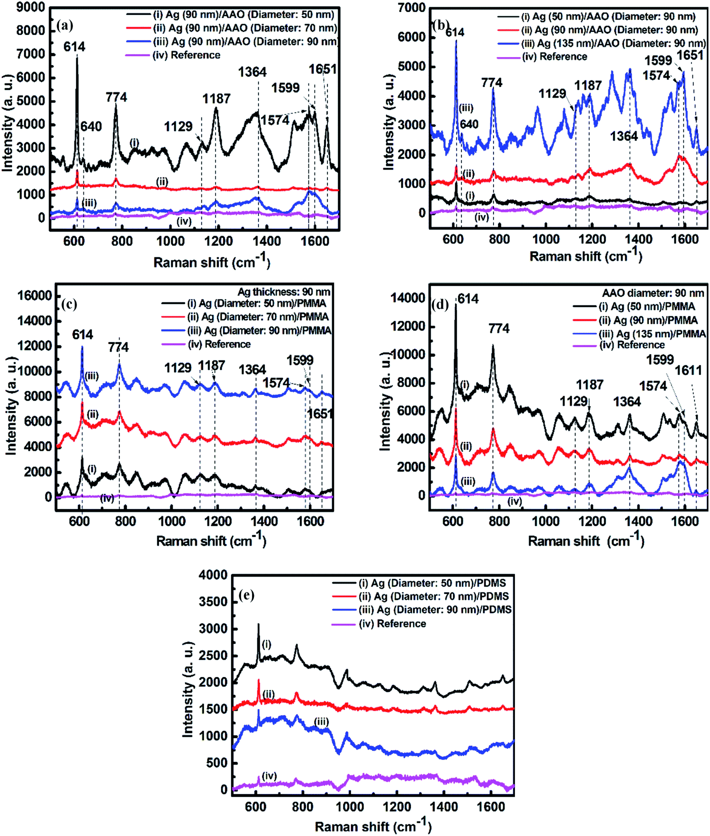
To theoretically analyze the experimental results of the pore size dependent enhancement effect, an electromagnetic simulation based on the finite-difference time-domain (FDTD) method was carried out. Using the 90 nm-thick Ag nanoporous films as one model, the EF change tendency was further correlated with the enhancement level of the electromagnetic field strength around the nanopores via a theoretical calculation of the surface electromagnetic field distribution in the nanoporous Ag thin film. Fig. 3a–c and d–f show the calculated surface electromagnetic field results for the 90 nm-thick Ag nanoporous films transferred from the AAO templates with diameters of 50 nm, 70 nm, and 90 nm to the PMMA and PDMS templates prepared via the invented template-assisted sol–gel inverse-imprinting process. Their relative maximum values (E/E0) of electromagnetic field strength are summarized in Table 2. For the Ag/PDMS samples, the electromagnetic field on the surface of the sample increased with an increase in the pore size (within 100 nm) (Fig. 3a–c). However, the field strength has different effects on the Ag/PMMA samples. The opposite electric field distribution results in the opposite tendency of the enhancement of the SERS intensities as the pore size changes. The experimental results are in perfect agreement with the simulation results, indicating that the electromagnetic enhancement in the Ag nanopore thin films plays a key role in the SERS performance of the samples. These opposite results induced by the different pore nanostructures show a pathway to pore nanostructure design for potential applications in the fabrication of meta-surfaces for controlling the polarization, phase, amplitude, and electrical field distribution.
 | ||
| Fig. 3 Calculated electromagnetic field distribution of the porous nano-silver film at a Raman excitation wavelength of 532 nm using the FDTD method. Shown are the 90 nm-thick nanoporous Ag films transferred from AAO templates with diameters of (a) 50, (b) 70, and (c) 90 nm to the PMMA substrates. Also shown are the 90 nm-thick nanoporous Ag films transferred from the AAO templates with diameters of (d) 50, (e) 70, and (f) 90 nm to the PDMS substrates. | ||
| Film thickness (nm) | 90 | 90 | 90 |
| Pore size (nm) | 50 | 70 | 90 |
| Relative strength (E/E0) of the Ag/PMMA sample | 6.24 | 7.05 | 7.96 |
| Relative strength (E/E0) of the Ag/PDMS sample | 6.02 | 5.21 | 4.14 |
Experimental
The porous AAO/Al substrate was first fabricated using a two-step anodization process.69 It is typically challenging to confirm the film thickness on AAO template. However, conventionally, researchers often deposit films on AAO and a smooth substrate (e.g., glass and wafer, respectively) with the same deposition time. The film thickness on the smooth substrate is then characterized using an optical ellipsometer or AFM method. In our experiment, we used this method to describe the film thickness on AAO. Then, the first type of sample supported on the AAO/Al templates was obtained by depositing the silver films at a thickness of 90 nm on top of the AAO/Al templates (pore length: 300 nm; inter-pore spacing: 110 nm) with pore diameters of 50, 70, and 90 nm using the magnetron sputtering (MSP-300 C) method at room temperature at a base pressure of 4.7 × 10⁻⁴ Pa.43 During the deposition process, the metallic Ag target (purity > 99.99%) was sputtered in a 15 mTorr Ar gas atmosphere using a direct current (DC) sputtering apparatus with a power density of 2.5 W cm−2. The second type of sample supported on the AAO/Al templates was prepared by depositing Ag silver films with thicknesses of 50, 90, and 135 nm on the top surface of the same type of AAO/Al templates with a pore diameter of 90 nm, a pore length of 300 nm, and inter-pore spacing of 110 nm. The sample obtained using the above procedures consisted of three layers: the bottom layer was an Al film, the middle layer was an AAO template, and the uppermost layer was an arrayed silver film.Fig. 4 illustrates the schematic fabrication process of the Ag/PMMA and Ag/PDMS substrates. First, the uppermost surfaces of the samples were spin-coated with PMMA (AR) and PDMS solutions, respectively, by using a spin coater (KW-4 A Type, 600 rpm). Before this process, a PDMS-based agent and curing agent were mixed with a mass ratio of 10![[thin space (1/6-em)]](https://www.rsc.org/images/entities/char_2009.gif) :1 to form a PDMS solution.70 (ii). After drying at 333 K in an oven for 3 h, the samples were attached to the PMMA and PDMS templates, respectively. Then, the dried samples were immersed in a 10 wt% HCl solution until the AAO templates were removed. After the deionized water washing process, the Ag/PMMA (iii-a) and Ag/PDMS (iii-b) samples were finally obtained.
:1 to form a PDMS solution.70 (ii). After drying at 333 K in an oven for 3 h, the samples were attached to the PMMA and PDMS templates, respectively. Then, the dried samples were immersed in a 10 wt% HCl solution until the AAO templates were removed. After the deionized water washing process, the Ag/PMMA (iii-a) and Ag/PDMS (iii-b) samples were finally obtained.
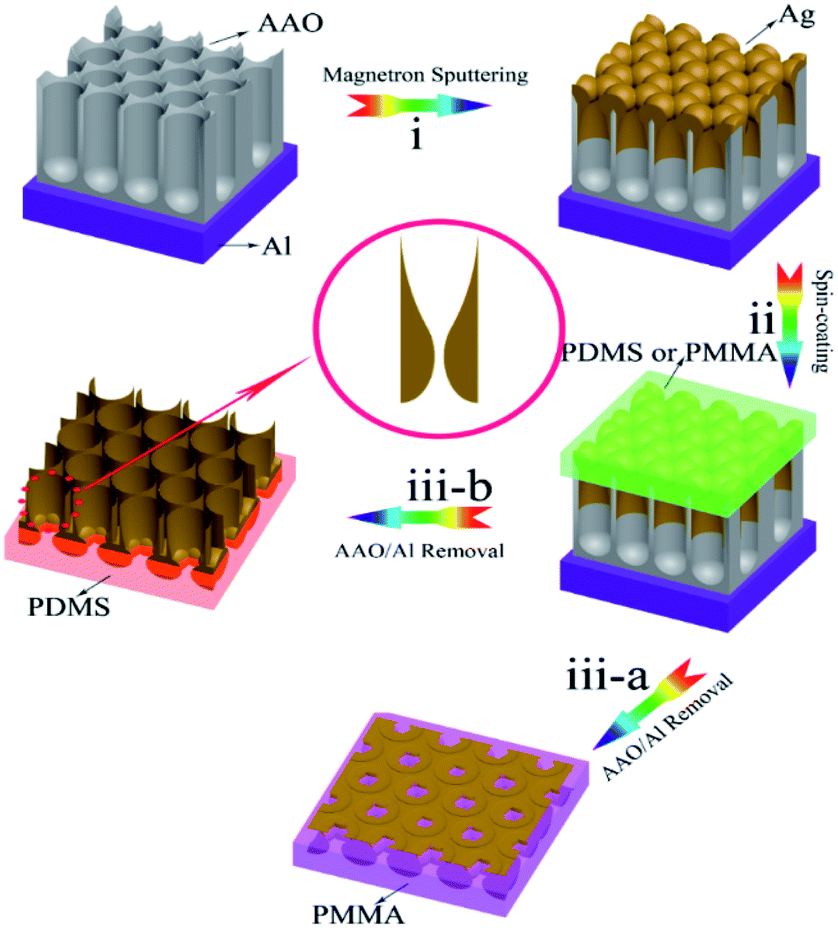 | ||
| Fig. 4 Schematic of the fabrication process. (i) Deposition of the Ag film on the AAO/Al template to form the AAO/Al-based Ag nanoporous arrays; (ii) spinning of PDMS and PMMA solutions onto the AAO/Al template; (iii) removal of the AAO/Al template to obtain the nanoporous Ag film supported on the PDMS and PMMA substrates. | ||
The morphologies were characterized using field emission scanning electron microscopy (FE-SEM, SUPRA-55). The absorption spectra of the nano-silver film with a uniform and ordered surface hole array were collected using a UV-Vis-NIR spectrophotometer (PerkinElmer, UV 950).
Before performing SERS measurements of the arrayed nanoporous thin films, the R6G aqueous solution was prepared using distilled deionized water. Then, the samples were first immersed in an R6G (BR 99.5%) solution at a concentration of 10−6 mol L−1 for 3 h to ensure the adsorption of molecules on the substrates, and then the substrates were dried at room temperature. To evaluate the performance of the above mentioned SERS substrates, we prepared an R6G solution with a concentration of 10−2 mol L−1 adsorbed on PMMA and PDMS substrates as references. The SERS spectra were recorded using a micro-confocal Raman spectrometer (HR 800) with an excitation wavelength of 532 nm. For this measurement, the single wavenumber range was scanned from 500 cm−1 to 1700 cm−1, and the Raman signal for a reasonably longer integration time was 5 s. The SERS EF was calculated according to the experimental data using eqn (1).
The FDTD method was used to calculate the electric fields of the Ag nanostructures that were supported on that PMMA and PDMS substrates. The circularly polarized light at normal incidence was along the z-axis. The electric field distributions were evaluated at 532 nm. The diagonal elements of the permittivity tensor obey the Drude model
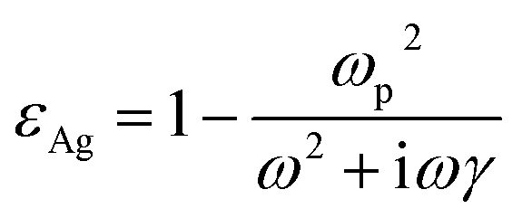 | (2) |
Conclusions
In summary, we prepared an AAO substrate using a two-step anodization method and then obtained a nanoporous Ag film on the AAO substrate using the magnetron sputtering method. Subsequently, the nanoporous Ag film was imprinted onto the transparent PMMA and PDMS substrates via the newly invented template-assisted sol–gel inverse-imprinting process. We showed that the SERS performance of the nanoporous thin film on the transparent PMMA and PDMS substrates could be considerably enhanced, and the enhancement tendency was differently elucidated according to the opposite electric field distribution around the nanopores with the increase in pore size, which was further confirmed by the field simulation using the FDTD method. In particular, the EF value can be up to 106 when the Ag thickness is chosen to be 50 nm based on pore diameters of 90 nm on the Ag/PMMA samples. This result may open an avenue for SERS research in the chemical/biosensing field, particularly enhanced sensitivity for DNA detection. This study also offers a facile and low-cost route to prepare highly sensitive and reproducible SERS substrates, which ultimately meet the rapidly increasing demand for the preparation of high through-put and ultra-sensitive detectors.Conflicts of interest
There are no conflicts to declare.Acknowledgements
This study was financially supported by BRICS STI Framework Programme by NSFC (No. 51861145309); National S&T Major Project of China (No. 2018ZX10301201); the National Natural Science Foundation of China (No. 51971029 and No. 51371018); the “1125” Zhihui Zhengzhou Talent project of Henan Province (No. 39080070) , the “100 talent plan” fund of Fujian Province (No. 39080067) and Postdoctor Research Foundation of Shunde Graduate School of University of Science and Technology Beijing (No. 2020BH005).Notes and references
- L. Guerrini and R. A. Alvarez-Puebla, Vibrational Spectroscopy in Protein Research, 2020, pp. 553–567 Search PubMed.
- S. Dong, Y. Wang, Z. Liu, W. Zhang, K. Yi, X. Zhang, X. Zhang, C. Jiang, S. Yang, F. Wang and X. Xiao, ACS Appl. Mater. Interfaces, 2020, 12, 5136–5146 CrossRef CAS PubMed.
- C. Byram, S. S. B. Moram and V. R. Soma, Analyst, 2019, 144, 2327–2336 RSC.
- H. Feng, F. Yang, J. Dong and Q. Liu, RSC Adv., 2020, 10, 11865–11870 RSC.
- R. Prabhu, K. Bramhaiah and N. S. John, Nanoscale Adv., 2019, 2426–2434 RSC.
- S. Ganesh, K. Venkatakrishnan and B. Tan, Nat. Commun., 2020, 11, 1135 CrossRef CAS PubMed.
- Y. Si, L. Xu, N. Wang, J. Zheng and J. Li, Anal. Chem., 2020, 93, 2649–2655 CrossRef PubMed.
- B. M. Crawford, P. Strobbia, H.-N. Wang, R. Zentella, M. I. Boyanov, Z.-M. Pei, T.-p. Sun, K. M. Kemner and T. Vo-Dinh, ACS Appl. Mater. Interfaces, 2019, 11, 7743–7754 CrossRef CAS PubMed.
- N. Jiang, Y. Hu, W. Wei, T. Zhu and M. Yu, Microchim. Acta, 2019, 186, 65 CrossRef PubMed.
- J. Liu, T. Zheng and Y. Tian, Angew. Chem., Int. Ed., 2019, 58, 7757–7761 CrossRef CAS PubMed.
- Z. Qian, J. Fei, S. Zong, K. Yang, L. Li, R. Liu, Z. Wang and Y. Cui, ACS Sens., 2020, 5, 208–216 CrossRef CAS PubMed.
- C. Credi, O. Bibikova, C. Dallari, B. Tiribilli and F. S. Pavone, J. Mater. Chem. B, 2020, 8, 1629–1639 RSC.
- C. Xu, D. Cao, W. Lu, J. Sun and S. Cheng, New J. Chem., 2013, 1–3 Search PubMed.
- V. M. Papadakis and G. Kenanakis, Appl. Phys. A: Mater. Sci. Process., 2018, 124, 9 CrossRef.
- N. Hanagata, Int. J. Nanomed., 2017, 12, 515–531 CrossRef CAS PubMed.
- W. Zhang, X. Zhao, Y. Yuan, F. Miao, W. Li, S. Ji, X. Huang, X. Chen, D. Weitz and Y. Song, Chem. Mater., 2020 Search PubMed.
- E. Akanny, A. Bonhommé, C. Commun, A. Doleans-Jordheim, C. Farre, F. Bessueille, S. Bourgeois and C. Bordes, J. Raman Spectrosc., 2020, 51, 619–629 CrossRef CAS.
- A. Bhattarai, Z. Cheng, A. G. Joly, I. V. Novikova and P. Z. El-Khoury, J. Phys. Chem. Lett., 2020, 11, 1795–1801 CrossRef CAS PubMed.
- M. B. Hillyer, S. Nam and B. D. Condon, J. Nanopart. Res., 2020, 22, 42 CrossRef CAS.
- I. C. Kuschnerus, M. Lau, K. Giri, N. M. Bedford and A. Garcia-Bennett, Nanoscale, 2020, 12, 5898–5905 RSC.
- A. Miri, M. Sarani and M. Khatami, RSC Adv., 2020, 10, 3967–3977 RSC.
- K. Xin, X. Shi, Y. Liu, Z. Zhang and J. Ma, Opt. Express, 2020, 8734–8743 CrossRef PubMed.
- M. Yan, Y. She, X. Cao, J. Ma and J. Wang, Microchim. Acta, 2019, 186, 143 CrossRef PubMed.
- M. Dehurtevent, L. Robberecht, A. Thuault, E. Deveaux and P. Béhin, J. Prosthet. Dent., 2020 Search PubMed.
- J. Hwang and M. Yang, Sensors, 2018, 18, 4076 CrossRef PubMed.
- A. Purwidyantri, C.-H. Hsu, B. A. Prabowo, C.-M. Yang and C.-S. Lai, IOP Conference Series Earth and Environmental Science, 2019, vol. 277, p. 012034 Search PubMed.
- V. Suresh, L. Ding, A. B. Chew and F. L. Yap, ACS Appl. Nano Mater., 2018, 1, 886–893 CrossRef CAS.
- N. Félidj, J. Aubard, G. Lévi, J. R. Krenn, M. Salerno, G. Schider, B. Lamprecht, A. Leitner and F. R. Aussenegg, Phys. Rev. B: Condens. Matter Mater. Phys., 2002, 65, 075419 CrossRef.
- K. M. Baek, J. Kim, S. Kim, S. H. Cho, M. S. Jang, J. Oh and Y. S. Jung, Chem. Mater., 2018, 30, 6183–6191 CrossRef CAS.
- H. Li, D. Men, Y. Sun, D. Liu, X. Li, L. Li, C. Li, W. Cai and Y. Li, J. Colloid Interface Sci., 2017, 505, 467–475 CrossRef CAS PubMed.
- L. Lin, Q. Zhang, X. Li, M. Qiu, X. Jiang, W. Jin, H. Gu, D. Y. Lei and J. Ye, ACS Nano, 2018, 12, 6492–6503 CrossRef CAS PubMed.
- J. Quan, Y. Zhu, J. Zhang, J. Li and N. Wang, Appl. Opt., 2017, 56, 5751–5760 CrossRef CAS PubMed.
- J.-Y. Kim, D. Han, G. M. Crouch, S.-R. Kwon and P. W. Bohn, Anal. Chem., 2019, 91, 4568–4576 CrossRef CAS PubMed.
- R. Liu, T. Sha and B. Nie, Anal. Methods, 2019, 11, 171–178 RSC.
- G. Itami and O. Sakai, J. Appl. Phys., 2019, 125, 213101 CrossRef.
- S. J. Heerema, L. Vicarelli, S. Pud, R. N. Schouten, H. W. Zandbergen and C. Dekker, ACS Nano, 2018, 12, 2623–2633 CrossRef CAS PubMed.
- J. Li, D. Stein, C. Mcmullan, D. Branton, M. J. Aziz and J. A. Golovchenko, Nature, 2001, 412, 166–169 CrossRef CAS PubMed.
- C. Dekker, Nat. Nanotechnol., 2007, 2, 209–215 CrossRef CAS PubMed.
- J. Sun, L. Gong, Z. Gong, D. Wang, X. Yin and M. Fan, Anal. Methods, 2019, 11, 4917–4922 RSC.
- Z. Bai-chuan, L. Ya and Z. Cong-yun, Journal of Liaocheng University, 2019, 32, 63–68 Search PubMed.
- C. Zhao, Y. Zhu, L. Chen, S. Zhou, Y. Q. Su, X. Ji, A. Chen, X. Gui, Z. Tang and Z. Liu, Nanoscale, 2018, 10, 16278–16283 RSC.
- W. Zhang, J. Li, X. Ding, P. Pernod, N. Tiercelin and Y. Song, Sci. Rep., 2017, 7, 2888 CrossRef PubMed.
- W. Zhang, Q. Wang, C. Zhao and Y. Song, Opt. Commun., 2019, 437, 44–49 CrossRef CAS.
- W. Zhang, Y. Wang, Q. Wang, V. I. Belotelov and Y. Song, J. Phys. Chem. C, 2018, 122, 29457–29463 CrossRef CAS.
- W. W. Zhang, Z. H. Liu, V. I. Belotelov, Q. Wang and Y. J. Song, Thin Solid Films, 2018, 660, 301–305 CrossRef CAS.
- Z. Lu-Bin, Y. Jun, Z. Yu-Ming, L. Qing, C. Xiao-Xia and L. Fang-Hong, Anal. Chem., 2014, 86, 6262–6267 CrossRef PubMed.
- Z. Honghua, L. Mao, Z. Fei, L. Dilong, L. Guangqiang, D. Guotao, C. Weiping and L. Yue, Small, 2015, 11, 844–853 CrossRef PubMed.
- M. Luo, H. Huang, S. I. Choi, C. Zhang, S. R. Da, H. C. Peng, Z. Y. Li, J. Liu, Z. He and Y. Xia, ACS Nano, 2015, 9, 10523–10532 CrossRef CAS PubMed.
- X. Liu, L. Li, Y. Yang, Y. Yin and C. Gao, Nanoscale, 2014, 6, 4513–4516 RSC.
- A. Alyami, A. J. Quinn and D. Iacopino, Talanta, 2019, 201, 5864 CrossRef PubMed.
- J. E. George, V. K. Unnikrishnan, D. Mathur, S. Chidangil and S. D. George, Sens. Actuators, B, 2018, 272, 485–493 CrossRef CAS.
- A. R. Paschoal, N. L. M. Costa, R. A. Domingues and E. B. Santos, Mater. Lett., 2019, 255, 126557 CrossRef CAS.
- H. Qiu, M. Wang, S. Jiang, L. Zhang, Z. Yang, L. Li, J. Li, M. Cao and J. Huang, Sens. Actuators, B, 2017, 249, 439–450 CrossRef CAS.
- C. Wang, J. Zhang, M. Xu, J. Xiang, Y. Wu and T. Xu, Mater. Res. Express, 2019, 6, 8 Search PubMed.
- B. Ying, C. Lai, Z. Zhu, F. Hao and C. Jiang, RSC Adv., 2013, 3, 8998–9004 RSC.
- X. Zhao, J. Yu, C. Zhang, C. Chen and S. Xu, Appl. Surf. Sci., 2018, 455, 1171–1178 CrossRef CAS.
- A. Alyami, A. J. Quinn and D. Iacopino, Talanta, 2019, 201, 58–64 CrossRef CAS PubMed.
- R. Das and R. K. Soni, Appl. Surf. Sci., 2019, 489, 755–765 CrossRef CAS.
- X. Xu, Opt. Commun., 2001, 199, 89–93 CrossRef CAS.
- X. Xingsheng, M. Hai, Z. Qijing and Z. Yunsheng, J. Opt. A: Pure Appl. Opt., 2002, 4, 237–242 CrossRef.
- F. Pallikari, G. Chondrokoukis and M. Rebelakis, Mater. Res. Innovations, 2001, 4, 89–92 CrossRef CAS.
- K. J. Thomas, M. Sheeba, V. P. N. Nampoori, C. P. G. Vallabhan and P. Radhakrishnan, J. Opt. A: Pure Appl. Opt., 2008, 10, 055303 CrossRef.
- J. Chen, J. Li, L. Xu, W. Hong and Y. Yang, Polymers, 2019, 11, 601 CrossRef PubMed.
- P. Hildebrandt and M. Stockburger, J. Phys. Chem., 1984, 88, 5935–5944 CrossRef CAS.
- V. S. Tiwari, T. Oleg, G. K. Darbha, W. Hardy, J. P. Singh and P. C. Ray, Chem. Phys. Lett., 2007, 446, 77–82 CrossRef CAS.
- M. L. Coluccio, G. Das, F. Mecarini, F. Gentile, A. Pujia, L. Bava, R. Tallerico, P. Candeloro, C. Liberale and F. D. Angelis, Microelectron. Eng., 2009, 86, 1085–1088 CrossRef CAS.
- K. H. Yang, Y. C. Liu and C. C. Yu, J. Mater. Chem., 2008, 18, 4849–4855 RSC.
- D. Shan, L. Huang, L. Xin, W. Zhang and Z. Yu, J. Phys. Chem. C, 2014, 118, 23930–23936 CrossRef CAS.
- H. Masuda and M. Satoh, Jpn. J. Appl. Phys., 2014, 35, L126–L129 CrossRef.
- V. T. Nguyen, B. K. Min, Y. Yi, S. J. Kim and C. G. Choi, Chem. Eng. J., 2020, 393, 10 CrossRef.
- M. G. Blaber, M. D. Arnold and M. J. Ford, Vibrational Spectroscopy in Protein Research, 2009, vol. 113, pp. 3041–3045 Search PubMed.
- Refractive index database, http://refractiveindex.info/ Search PubMed.
Footnote |
| † Electronic supplementary information (ESI) available: Supporting figure (Fig. S1). See DOI: 10.1039/d0ra03803b |
| This journal is © The Royal Society of Chemistry 2020 |