 Open Access Article
A coupled model of electromagnetic and heat on nanosecond-laser ablation of impurity-containing aluminum alloy
Jiaheng Yin ,
Yongzhi Cao
 *,
Yongda Yan
 ,
Lihua Lu,
Jiaxuan Chen and
Fuli Yu
Center for Precision Engineering, Harbin Institute of Technology, Harbin, 150001, China. E-mail: cflying@hit.edu.cn; Fax: +86-451-86415244; Tel: +86-451-86412924
First published on 20th August 2020
Abstract
In the emerging field of laser-driven inertial confinement fusion, Joule heating generated via electromagnetic heating of the metal frame is a critical issue. However, there are few reported models explaining thermal damage to the aluminum alloy. The aim of this study was to build a coupled model for electromagnetic radiation and heat conversion of an ultrashort laser pulse on an aluminum alloy based on Ohm's law. Additionally, the application SiO2 films on aluminum alloy to improve the laser-induced damage threshold (LIDT) were simulated, and the effects of metal impurities in the aluminum alloy were analyzed. A model examining the relation between electromagnetic radiation and heat for a nanosecond laser irradiating an aluminum alloy was developed using a coupled model equation. The results obtained using the finite difference time domain (FDTD) algorithm can provide a theoretical basis for future improvement of the aluminum alloy LIDT.
1. Introduction
Laser-driven inertial confinement fusion (ICF) can generate large amounts of renewable energy via the chemical reaction of two forms of hydrogen—deuterium (D) and tritium (T)1—and the reaction is expressed in eqn (1). However, the half-life of tritium (T) is short and it does not occur naturally; furthermore, it is extremely difficult to obtain via reaction. Hence, tritium in fusion reactors needs to be recycled, using doubled neutrons for reaction with lithium followed by recovery of tritium, where tritium functions like a catalyst (reaction shown in eqn (2)).2 Because of its potential advantages for quickly generating a large, inexhaustible amount of clean energy.3–5 A nuclear laser facility can reach 1.8 MJ and 500 TW of 355 nm light in 10−9 s, which is equivalent to 1000 times the energy consumption of the United States.6 The French Megajoule Laser Project (LMJ) supported by the French Atomic Energy Commission (CEA)7 and the American National Ignition Facility Project (NIF) are collaborating with Lawrence Berkeley National Laboratory8 to realize this goal. For this process, damage to optical elements such as fused silica and potassium dihydrogen phosphate (KDP) is an important topic of research.9,10 However, laser-induced damage of the aluminum alloy frame for the entire system has not been comprehensively studied, especially via theoretical research.| 21D + 31T → 42He (3.5 MeV) + 0n (14.1 MeV) | (1) |
| 0n + 63Li → 31T + 42He + 4.784 MeV | (2) |
The traditional laser power conversion configuration is usually applied to photovoltaic (PV) cells. Light-to-heat generation and light-to-electricity conversion have recently seen research progress.11,12 Previous work aimed at improving the efficiency between the input power and the power output by the battery, and some studies attributed the low ceiling to the temperature.13,14 While laser-induced damage in dielectrics is related to the pulse duration, there are qualitative differences between multi-photon ionization and Joule heating, which include plasma formation and conventional melting.15 The energy coupling mechanism between an ultrashort pulse laser and optical materials has become an issue of intense research interest, including the exploration of surface damage initiation,16 the optical breakdown process,17 electronic excitation–relaxation processes,18 and particle generation.19 Studies have been limited to either experimental or single-simulation investigation of the influence of the pulse duration,20 laser fluence, and wavelength21 on site damage or the morphology of the optical elements. The impact of the electric-field distribution on field enhancement was simulated22 and a temperature model was established to analyze the interaction between the laser and metallic materials.23 To investigate impurities present in the crystals, Bhar et al. studied the LIDT and the effect of inclusions in some nonlinear crystals; they found that Na+ ion inclusion and the LIDT of the BBO crystals were correlated.24 Some studies investigated the laser-induced damage threshold (LIDT) of the TiO2/SiO2 multilayer reflective coatings and determined the ultra-short LIDT of KH2PO4 via simulation. They studied the effects of lasers of different wavelengths on the optical properties of dielectric materials experimentally and via simulations.25,26 This research was aimed at studying the laser damage threshold, the reflectivity curve of a TiO2 single-layer film (experimentally and fitted), and the GIXRD of SiO2 and TiO2 single layers. However, the relationship between the laser fluence and the temperature was not investigated in detail. Hence, the search for a coupled model for electromagnetic radiation and heat conversion during nanosecond-laser ablation of aluminum alloy is still an unresolved issue.
Moreover, energy conversion resulting in laser-induced damage of a thin film has not been widely studied, and other aspects of thin films used for PV cells have generally received more attention. For example, the double-pulse temporal method was applied to a thin foil film, the results showed that the energy conversion efficiency was 15% higher than with a single pulse,27 and Cu2ZnSnS4 thin films are widely applied in solar cells. These studies focused more on pulsed laser film deposition,28 energy conversion efficiency,29 and the fabrication of thin films.30 Silica is used in optical elements because of its antireflection properties in high-power laser systems, which can improve the LIDT of the optical components.31,32 Studies have mostly been confined to the laser parameters, including the pulse duration,33 laser fluence,34 and wavelength,35 as well as to the film processing parameters including the thickness and organic groups36 that affect the growth of the silica thin film, such as its morphology and growth rate. However, studies have not modeled the relation between electromagnetic radiation and heat in the silicon dioxide thin films. Therefore, a coupled model that is related to the aluminum alloy and the silicon dioxide thin film used as a surface coating needs to be investigated; this should extend beyond the relation between electromagnetic radiation and heat and also include the silicon dioxide film and its substrate.
In this work, a coupled model was built for electromagnetic radiation and heat conversion in an aluminum alloy with a nanosecond-laser. We first investigated the effect of copper impurities at a certain depth in the aluminum alloy under UV laser irradiation via FDTD simulations. Then, the light-to-electricity conversion was studied. The results of the light intensity enhancement factor (LIEF) of the aluminum alloy before and after coating with the SiO2 thin films were determined. Finally, the effect of metal impurities (copper and aluminum) in the aluminum alloy on the temperature rise was simulated and the conclusions are outlined.
2. Coupled geometric modeling of electromagnetic and heat
The coupled model of electromagnetic radiation and heat was based on Ohm's law. Electromagnetic radiation to heat conversion in the structure can be assigned to the response to ohmic loss and Joule heating. The power dissipated is equivalent to:| P = J × E, | (3) |
| Q = εω0Im|E(r)|2, | (4) |
| ∮H × dl = ∫J × ds. | (5) |
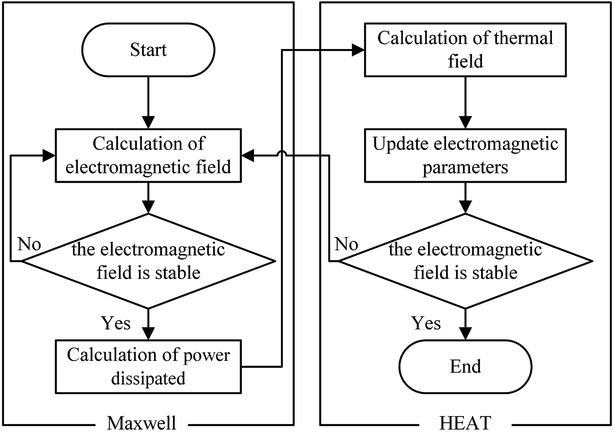
The calculation flow chart for the coupled model of electromagnetic radiation and heat on nanosecond-laser ablation is presented in Fig. 1. The steps to simulate the electromagnetic radiation to heat conversion using the coupled model is as follows:
• Step 1: after irradiation with a high-fluence nanosecond laser, the electromagnetic field was first calculated until the field reached a steady-state inside the object.
• Step 2: the power, which dissipated because of ohmic loss, was next calculated based on eqn (3), which was then applied to the heat transport equations as the heat energy transfer rate.
• Step 3: once the desired simulation time was reached, the simulation was stopped.
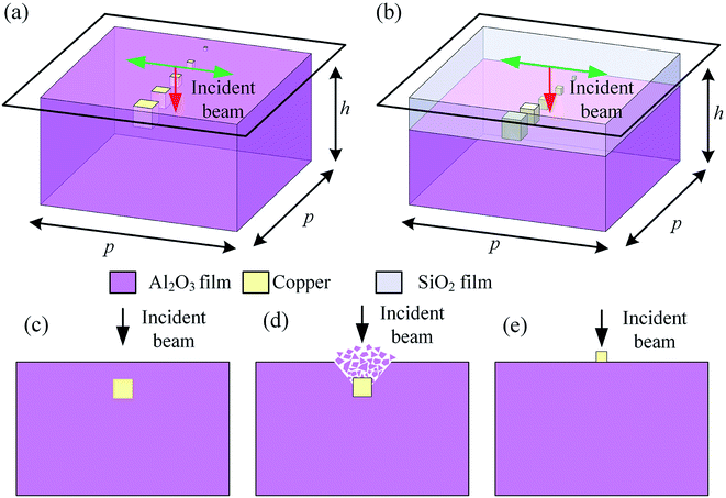
Fig. 2 shows the process used to obtain the coupled model for the electromagnetic field and heat during nanosecond laser ablation. It can be seen from Fig. 2(a) and (b) that the thickness of the aluminum alloy for its own micro arc oxide layer and after coating with a silicon dioxide thin film remains consistent (h = 10 μm). Fig. 2(c)–(e) show the laser-induced damage process for the thin films doped with metal particles. The plasma formation and ablation first happened as shown in Fig. 2(a), and then the metal particles were exposed to air; for an irradiation time > 100 ps, both the particles and substrate were subject to conventional melting and boiling, as seen from Fig. 2(b). Because the temperature rise of the metal particles was faster, the temperature changes of the metal particles were primarily simulated after being exposed to air (see Fig. 2(c)).
3. Discussion and numerical simulation
3.1 Spectral characteristics of Al2O3 before and after coating with a SiO2 thin film
The electric-field intensity in Al2O3 before and after coating with a silicon thin film was simulated using the FDTD method. To ensure accurate results for the simulation, the simulation domain was gridded with spacings at 12 samples per wavelength according to the Courant stability condition. Furthermore, to ensure uniformity of film thickness for each layer, the x- and y-directions adopted periodic boundary conditions while the z-direction adopted a perfectly matched layer-absorbing boundary condition.The spectral characteristics took the form of a plane wave as the initial condition and the incident direction was in the z-direction at a normal incidence of 1.064 μm. According to the Fresnel reflection theory, a formula for calculating the transmission coefficient of the TE mode material at normal incidence can be expressed as follows.
 | (6) |
 | (7) |
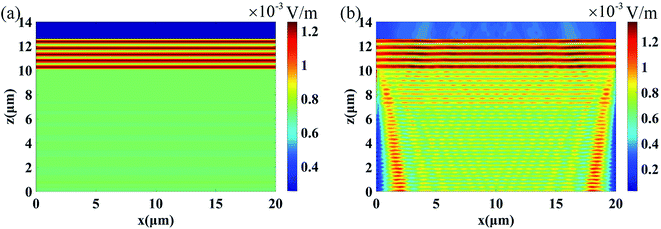 | ||
| Fig. 3 FDTD simulation results for the TE mode E distribution at a normal incidence for non-metal doped (a) Al2O3 and (b) SiO2 thin films. | ||
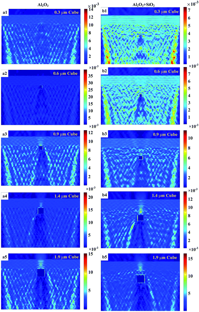
Fig. 4 shows the light intensity distributions for the Al2O3 thin films before and after coating with the SiO2 thin films with mental copper cube particles of edge lengths 0.3, 0.6, 0.9, 1.4, and 1.9 μm. The differences in the light intensity distributions with the SiO2 thin film coatings were not remarkable. The light intensity enhancement factor (LIEF) is widely applied to characterize the intensity enhancement of an aluminum alloy before and after coating by thin films with metal particles:
 | (8) |
| Cube (μm) | Al2O3 | SiO2 | ||
|---|---|---|---|---|
| E (V m−1) | LIEFs | E (V m−1) | LIEFs | |
| 0.3 | 1.9 | 6.9 | 1.5 | 3.4 |
| 0.6 | 3.0 | 17.3 | 1.6, 6.6 | 3.9 |
| 0.9 | 2.1 | 8.5 | 2.2 | 7.3 |
| 1.4 | 2.0 | 7.7 | 2.3 | 7.8 |
| 1.9 | 2.4 | 11.1 | 2.4 | 8.7 |
Differences in the LIEFs between the Al2O3 thin films and SiO2 thin films could be attributed to the different types chemical bonds in the two materials. Photo-ionization and impact ionization led to an increase in the free electron density, which destroyed the metal frame because of the interaction between the strong laser field and the dielectric materials. SiO2 is an atomic crystal, here, a Si atom forms four covalent bonds with four O atoms, while one oxygen atom forms two covalent bonds with two Si atoms. The covalent bond is a type of chemical bond, here, two or more atoms use their outer electrons to reach a state of electronic saturation under ideal circumstances. This makes for a relatively stable chemical structure. The valence bond is the interaction between atoms via the sharing of electron pairs. The ionic bond refers to a chemical bond between anions and cations formed via electrostatic interaction, which occurs after two or more atoms or chemical groups lose or gain electrons and become ions. An electrostatic interaction is present between oppositely charged ions. When two oppositely charged ions are close, they are attracted to each other; there is mutual electrostatic repulsion between electrons and electrons and the nuclei and nuclei, when the electrostatic attraction and repulsion reach an equilibrium, ionic bonds are formed. The melting and boiling points of the SiO2 atomic crystal are higher than those of Al2O3, which is an ionic crystal. This can explain the larger LIEF observed for the Al2O3 thin films than for the SiO2 thin films.
3.2 Electromagnetic radiation and heat model for impurities-containing Al2O3
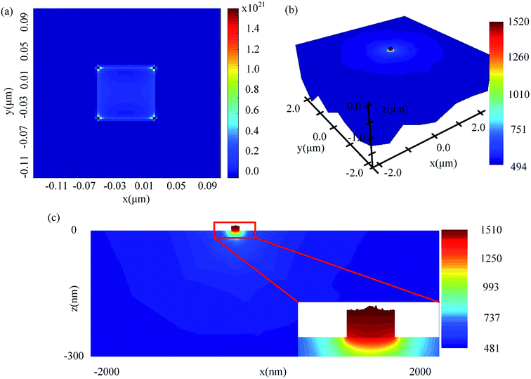
Fig. 5 shows the electromagnetic and heat model of Al2O3. For the structure in Fig. 5, the copper cube dimensions were 90 nm, and the Al2O3 substrate 20 μm × 20 μm × 10 μm was held at a laser fluence of Φ = 8 J cm−2 with a laser wavelength of 1064 nm. We first ran the simulation and visualized the absorbed power density profile (shown in Fig. 5(a)), and then the absorption data were loaded in the heat source. Once the simulation was carried out, the results were loaded in the HEAT solver region and the temperature was visualized in Fig. 5(b) and (c). The result of the coupled electromagnetic and heat model showed that the highest temperature for copper was 1520 K, which was above the melting point (1357.77 K) and led to damage of the material (see Fig. 5(c)).To investigate the effect of impurities on the temperature rise under different laser fluences (Φ), copper and aluminum cubes were placed in the Al2O3 substrate, with cube edge lengths between 50 and 90 nm in 10 nm intervals. The temperature rise curves are shown in Fig. 6(a) and (b), where the temperature rise (T) vs. laser fluence (Φ) is plotted. We can see that the temperature increased linearly with the laser fluence, as follows:
| T = kΦ + b, | (9) |
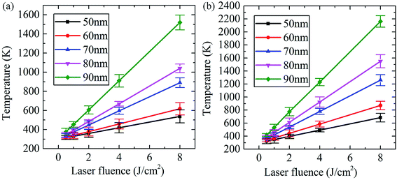 | ||
| Fig. 6 Temperature rises along with increasing laser fluence and edge length of (a) copper and (b) aluminum. | ||
| Cube (nm) | Copper | Aluminum | ||||
|---|---|---|---|---|---|---|
| k | b (K) | R2 | k | b (K) | R2 | |
| 50 | 29.61 | 300.21 | 0.99 | 48 | 300 | 1 |
| 60 | 39.59 | 300.08 | 0.99 | 71.35 | 300 | 0.99 |
| 70 | 73.74 | 300.00 | 0.99 | 120 | 300 | 1 |
| 80 | 92.52 | 299.58 | 0.99 | 156.26 | 299.58 | 1 |
| 90 | 152.49 | 300.08 | 1 | 232.09 | 303.7 | 0.99 |
Table 2 shows that the temperature growth coefficient (k) increased with increasing cube size. The temperature growth coefficient for the copper cubes was smaller than for aluminum cubes, with the former being approximately two-thirds of the latter. Furthermore, the growth rate of the growth coefficient (k) increased a lot with increasing cube edge length. For a copper cube with a side length of 50 nm, the k was 29.61, and the k went up to 152.49 for a length of 90 nm, which is ∼5 times larger. A similar trend was also observed for the aluminum cubes. Both of their constants (b) were ∼300 K, and the results fit extremely well.
Fig. 6 intuitively compares the temperature (T) growth calculated using Lumerical's DGTD solver. The linear fit shown on the plot indicates that the 60 nm-length aluminum-cube almost reached its melting point (933.16 K) at a laser fluence (Φ) of 8 J cm−2, which had a temperature of 871 K. However, the copper cube's temperature was only 617 K under the same conditions. When the side length of the copper cube was 90 nm, the temperature abruptly increased to 1520 K under 8 J cm−2 laser irradiation, which is approximately two times that at 4 J cm−2 (880 K). The reasons for the temperature response to laser fluence and edge-length between copper and aluminum could be attributed to their different melting points. The lower laser fluence can lead to an aluminum temperature of up to 890 K, and this temperature is far from the melting point of copper (1357.77 K). Additionally, aluminum is a type of active metal. Under laser irradiation, a series of collisions occur between energetic particles and the lattice atoms of the metal. Aluminum can easily lose its electrons and be damaged by irradiation.
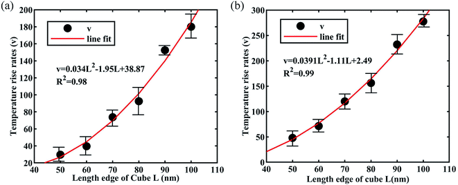
To validate the hypothesis that the rate of temperature rise is related to the edge length of the cubic impurities, we analyzed the average temperature rise rates (TRR). The TRR was calculated using the simulation. The growth curves for the relationship between the TRR and copper/aluminum cubes can be seen in Fig. 7(a) and (b). These graphs plot the TRR vs. cubes length (50–100 nm, 10 nm intervals). It can be seen from the graph that the TRR of the copper and aluminum cubes was similar, and that they could both take the form of a quadratic equation. However, as the laser fluence reached 8 J cm−2, the temperature of the 100 nm aluminum cube was 2520 K, while that of copper was 1740 K, hence, the TRR of the aluminum cube was larger than that of the copper cube. The reasons were previously explained and are mainly determined by the characteristics of the material itself.
4. Conclusion
In this paper, we investigated a coupled model for electromagnetic radiation and heat conversion in a metal frame for laser-driven inertial confinement fusion. The process of reacting deuterium (D) and tritium (T) could generate a large amount of clean and recyclable energy, and the success of the laser ignition process relies on a clean optical system. The proposed coupled model can guide the choice of laser fluence, provide a method to improve the LIDT of materials in the system, and reduce impurities in the laser system. This work could provide an effective theoretical reference to control the nuclear reaction. On the basis of the simulation, the specific conclusions can be summarized as follows.(1) The laser-induced damage threshold of the aluminum alloy could be improved by coating with a SiO2 thin film. The light intensity enhancement factor of Al2O3 thin films could be significantly reduced after surface treatment.
(2) The existence of metal impurities in the aluminum alloy could result in melting of the metal frame and may cause impurity contamination of the laser system. Furthermore, the contaminated-environment will reduce the efficiency of laser transmission and would eventually lead to a failure of ignition; hence, further research on the metal impurities in the aluminum alloy frame is important.
(3) The temperature growth of the aluminum alloy is related to the edge length of the metal cube. At the nanoscale (<100 nm), the temperature growth for a cube of a certain length was found to be linear with increasing laser fluence. With increasing cube length, the growth rate of the temperature was larger.
In this work, a coupled model was built to verify the laser induced damage threshold of an aluminum alloy frame before and after being coated with SiO2, and the results demonstrate the effect of nanoscale metal impurities on the temperature rise of the frame. It was shown that while metal impurities in the aluminum alloy frame were inevitable, surface treatment could provide effective protection and gives direction for the future design of such systems.
Nomenclatures
| 21D | Deuterium |
| H | Magnetic field |
| 21T | Tritium |
| r | Transmission coefficient |
| 21He | Helium |
| n1 | Refractive index of air |
| 0n | Neutron |
| n2 | Refractive index of materials |
| 63Li | Lithium |
| Et | Electric field under transmission wave of materials |
| P | Power dissipated |
| E0 | Normalized electric field |
| J | Current density |
| I | Light intensity value |
| E | Electric field |
| S | Poynting vector |
| Q | Heat energy transfer rate (W m−3) |
| μ | Magnetic permeability |
| ω0 | Angular frequency |
| T | Temperature |
| ε | Permittivity |
| Φ | Laser fluence (J cm−2) |
Conflicts of interest
There are no conflicts to declare.Acknowledgements
This work was supported by the National Key Research and Development Program of China (No. 2017YFA0701200), the State Key Program of National Natural Science Foundation of China (No. 51535003), the State Key Laboratory of Precision Measurement Technology and Instruments (No. PILAB1701).References
- J. Meyer-Ter-Vehn, S. Atzeni and R. Ramis, Rev. Sci. Instrum., 2010, 81, 10E531 CrossRef PubMed.
- H. Jie, K. Xiang-Shan, S. Jingjing, Y. Yu-Wei, W. Xuebang, C. S. Liu and S. Jun, Nucl. Fusion, 2018, 58, 096021 CrossRef.
- B. M. V. Wonterghem, C. A. Haynam, C. C. Widmayer, C. D. Marshall, C. D. Orth, E. Moses, G. M. Heestand, G. V. Erbert, J. Menapace and J. M. Auerbach, Appl. Opt., 2007, 46, 3276 CrossRef.
- E. I. Moses, Energy Convers. Manage., 2008, 49, 1795–1802 CrossRef CAS.
- E. I. Moses and T. N. Collaborators, Nucl. Fusion, 2013, 53, 104020 CrossRef.
- C. J. Stolz, Philos. Trans. R. Soc., A, 2011, 370, 4115–4129 CrossRef.
- M. L. André, Fusion Eng. Des., 1999, 44, 43–49 CrossRef.
- W. J. Hogan, E. I. Moses, B. E. Warner, M. S. Sorem and J. M. Soures, Nucl. Fusion, 2001, 43, 567–573 CrossRef.
- A. Rudenko, J. P. Colombier, S. Höhm, A. Rosenfeld, J. Krüger, J. Bonse and T. E. Itina, Sci. Rep., 2017, 7, 12306 CrossRef PubMed.
- M. J. Chen, J. Cheng, X. D. Yuan, W. Liao, H. J. Wang, J. H. Wang, Y. Xiao and M. Q. Li, Sci. Rep., 2015, 5, 14422 CrossRef CAS.
- J. U. Kim, S. Lee, S. J. Kang and T. I. Kim, Nanoscale, 2018, 10, 21555–21574 RSC.
- M. ElKabbash, A. Sousa-Castillo, Q. Nguyen, R. Mariño-Fernández, N. Hoffman, M. A. Correa-Duarte and G. Strangi, Adv. Opt. Mater., 2017, 5, 1700617 CrossRef.
- P. Singh and N. M. Ravindra, Sol. Energy Mater. Sol. Cells, 2012, 101, 36–45 CrossRef CAS.
- M. Theelen, A. Liakopoulou, V. Hans, F. Daume, H. Steijvers, N. Barreau, Z. Vroon and M. Zeman, J. Renewable Sustainable Energy, 2017, 9, 021205 CrossRef.
- B. Stuart, M. Feit, A. Rubenchik, B. Shore and M. Perry, Phys. Rev. Lett., 1995, 74, 2248 CrossRef CAS PubMed.
- N. Shen, J. D. Bude and C. W. Carr, Opt. Express, 2014, 22, 3393–3404 CrossRef.
- M. Mahdieh and M. Gharibzadeh, Opt. Laser Technol., 2012, 44, 1713–1721 CrossRef.
- N. S. Shcheblanov and T. E. Itina, Appl. Phys. A: Mater. Sci. Process., 2013, 110, 579–583 CrossRef CAS.
- P. Ge, C. Jiaxuan, L. Lihua, M. Xinxiang, D. Zhe and L. Daming, Aerosol Sci. Technol., 2020, 54, 342–352 CrossRef.
- R. A. Negres, M. A. Norton, D. A. Cross and C. W. Carr, Opt. Express, 2010, 18, 19966–19976 CrossRef CAS PubMed.
- H. Wan-Qing, H. Wei, W. Fang, X. Yong, L. Fu-Quan, F. Bin, J. Feng, W. Xiao-Feng, Z. Wan-Guo and Z. Xiao-Min, Chin. Phys. Lett., 2009, 26, 017901 CrossRef.
- X. Cheng, J. Zhang, T. Ding, Z. Wei, H. Li and Z. Wang, Light: Sci. Appl., 2013, 2, e80 CrossRef.
- Q. Bai, Y. Li, R. Shen, K. Zhang, X. Miao and F. Zhang, Molecular simulation and ablation property on the laser-induced metal surface, SPIE Proceedings Vol. 11063: Pacific Rim Laser Damage 2019: Optical Materials for High-Power Lasers, 2019, DOI:10.1117/12.2539865.
- G. C. Bhar, A. K. Chaudhary and P. Kumbhakar, Appl. Surf. Sci., 2000, 161, 155–162 CrossRef CAS.
- A. S. S. Kumar, N. Kishore, C. Mukherjee, R. Kamparath and S. Thakur, Indian J. Phys., 2020, 94, 105–115 CrossRef.
- J. Cheng, M. Chen, K. Kafka, D. Austin, J. Wang, Y. Xiao and E. Chowdhury, AIP Adv., 2016, 6, 2248 Search PubMed.
- C. M. Brenner, A. Robinson, K. Markey, R. Scott, R. Gray, M. Rosinski, O. Deppert, J. Badziak, D. Batani and J. Davies, Appl. Phys. Lett., 2014, 104, 081123 CrossRef.
- S. Vanalakar, G. Agawane, S. W. Shin, M. Suryawanshi, K. Gurav, K. Jeon, P. Patil, C. Jeong, J. Kim and J. Kim, J. Alloys Compd., 2015, 619, 109–121 CrossRef CAS.
- M. Han, W. Chen, H. Guo, L. Yu, B. Li and J. Jia, J. Power Sources, 2016, 318, 121–127 CrossRef CAS.
- K. Moriya, K. Tanaka and H. Uchiki, Jpn. J. Appl. Phys., 2007, 46, 5780 CrossRef CAS.
- X. Zhang, W. Lin, J. Zheng, Y. Sun, B. Xia, L. Yan and B. Jiang, J. Phys. Chem. C, 2018, 122, 596–603 CrossRef CAS.
- X. Liu, X. Lu, P. Wen, X. Shu and F. Chi, Appl. Surf. Sci., 2017, 420, 180–185 CrossRef CAS.
- H. H. Lim and T. Taira, Opt. Express, 2017, 25, 6302–6310 CrossRef CAS PubMed.
- L. Lamaignère, R. Diaz, M. Chambonneau, P. Grua, J.-Y. Natoli and J.-L. Rullier, J. Appl. Phys., 2017, 121, 045306 CrossRef.
- M. Chambonneau, J.-L. Rullier, P. Grua and L. Lamaignère, Opt. Express, 2018, 26, 21819–21830 CrossRef CAS PubMed.
- F. Chi, N. Pan, C. Ding, X. Wang, F. Yi, X. Li and J. Lei, Appl. Surf. Sci., 2019, 463, 566–572 CrossRef CAS.
- A. O. Govorov and H. H. Richardson, Nano Today, 2007, 2, 30–38 CrossRef.
- G. Baffou, R. Quidant and F. J. García de Abajo, ACS Nano, 2010, 4, 709–716 CrossRef CAS PubMed.
| This journal is © The Royal Society of Chemistry 2020 |

