 Open Access Article
Fabrication of ideally ordered TiO2 through-hole membranes by two-layer anodization
Takashi Yanagishita *a,
Haruto Hirosea,
Toshiaki Kondob,
Patrik Schmuki
 c and
Hideki Masudaa
aDepartment of Applied Chemistry, Tokyo Metropolitan University, 1-1 Minamiosawa, Hachioji, Tokyo 192-0397, Japan. E-mail: yanagish@tmu.ac.jp
bDepartment of Mechanical System Engineering, Aichi University of Technology, 50-2 Manori, Nishihasama-cho, Gamagori, Aichi 443-0047, Japan
cDepartment of Materials Science and Engineering WW4-LKO, University of Erlangen-Nuremberg, Martensstrasse 7, D-91058 Erlangen, Germany
First published on 12th October 2020
Abstract
Ideally ordered TiO2 through-hole membranes were obtained by a combination of Ti substrate pre-patterning and two-layer anodization. The Ti substrate was pre-patterned by Ar ion milling using ideally ordered porous alumina as an etching mask. Each concave pit formed by dry etching acted as an initiation site for hole development during anodization, and ideally ordered anodic porous TiO2 was produced by anodization using an electrolyte containing fluoride ions. Two-layered anodic porous TiO2 samples with different solubilities were formed by heat treatment for the crystallization of the first anodized oxide layer and a subsequent second anodization. The selective dissolution of the lower part of the two-layered porous TiO2 produced an ideally ordered TiO2 through-hole membrane. Using the present process, the repeated preparation of ideally ordered TiO2 membranes can be conducted because the ideally ordered concave array, which corresponds to the hole arrangement at the bottom of the detached TiO2 membrane, is maintained even after detaching the membrane. The obtained samples can be applied to various functional devices, such as photonic crystals and filtration membranes with photocatalytic properties.
Introduction
TiO2 through-hole membranes obtained from anodic porous TiO2 prepared by Ti anodization in an acidic electrolyte containing fluoride ions and subsequent through-holing has attracted much interest as a starting material for various functional optical devices owing to its high refractive index and photoactive properties.1–10 To optimize the properties of functional devices prepared using a TiO2 through-hole membrane, the control of its geometrical structures is required. This is because the performance of functional devices prepared using a TiO2 through-hole membrane depends on its geometrical structures, which include the hole arrangement and hole size uniformity. In particular, in the case of optical devices used to control the propagation of light based on the periodicity of the refractive index, as typified by photonic crystals, the preparation of ideally ordered TiO2 through-hole membranes with uniformly sized holes is essential.11,12 Previously, we reported that ideally ordered porous TiO2 could be obtained by the anodization of a Ti substrate with an ideally ordered concave array on its surface.13,14 This is because each concave pit formed by Ti substrate pretexturing through nanoimprinting using a mold acts as an initiation site for hole development during the initial stage of anodization. However, a high-throughput preparation of ideally ordered TiO2 is difficult by this process because the formation of a concave array of indents on the surface of a Ti substrate is required for each anodization. In this approach, the exhaustion of the mold used for nanoimprinting is a serious problem because Ti is a very hard metal. In our recent report, we described a new process, called two-layer anodization, for the high-throughput preparation of TiO2 through-hole membranes with a self-ordered hole arrangement.15 In this process, two-layered anodic porous TiO2 samples with different solubilities are formed by a combination of anodization and subsequent heat treatment. The selective dissolution of the lower oxide layer, which is formed by a second anodization of the sample after heat treatment to induce crystallization, allows the easy production of TiO2 through-hole membranes. The ordered concave indent array, which corresponds to the hole arrangement at the bottom of the ordered anodic porous TiO2, is transferred to the surface of the Ti substrate after detaching the TiO2 membrane. Using this process, a high-throughput preparation of self-ordered TiO2 through-hole membranes was achieved, i.e., the residual Ti substrate with ordered concave arrays could be used for the next anodization.In the present report, we describe the high-throughput preparation of ideally ordered TiO2 through-hole membranes by a combination of Ti substrate pretexturing and two-layer anodization. Using the present process, the repeated preparation of ideally ordered TiO2 through-hole membranes is expected from a single Ti substrate without mold exhaustion because the pretexturing pattern of the Ti substrate can be maintained. The obtained samples can be used for various functional optical devices requiring an ideally ordered hole arrangement.
Experimental
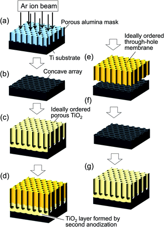
Fig. 1 shows a schematic drawing of the preparation process for ideally ordered TiO2 through-hole membranes. Prior to anodization, a Ti sheet was chemically polished using a commercially available chemical polishing solution (TCP-80, Mitsubishi Gas Chemical Co., Japan). In the present study, an ideally ordered concave array was formed on the surface of a Ti substrate by Ar ion milling using a porous alumina mask. The porous alumina mask was prepared by pretexturing Al using a Ni mold with an ordered indent array of 200 nm period and subsequent anodization under a constant voltage of 80 V in 0.05 M oxalic acid at 0 °C for 5 min. After anodization, the hole size of the anodic porous alumina was increased by wet etching in 10 wt% phosphoric acid at 30 °C for 20 min. A porous alumina mask was then obtained by the removal of residual Al in a saturated iodine methanol solution at 50 °C for 30 min. For the through-holing of the alumina mask, the bottom of the alumina layer was etched by Ar ion milling. The obtained thin porous alumina mask was placed on the Ti substrate. The Ar ion milling of the sample was carried out at 5 kV for 150 min. After pre-patterning the Ti substrate by Ar ion milling, the alumina mask was removed in a mixed solution of 1.8 wt% chromic acid and 6 wt% phosphoric acid. The anodization of Ti was performed under a constant voltage of 80 V in an ethylene glycol electrolyte containing 0.38 wt% NH4F and 10 wt% H2O at 20 °C for 20 min. To reduce the solubility of the oxide layer formed by the first anodization, the anodized sample was heat-treated at 300 °C for 1 h. The second anodization was performed under the same conditions as the first anodization. The anodic charge (electrical current × time) of the second anodization was adjusted to 1.0 mA h cm−2 to control the thickness of the oxide layer formed by the second anodization. An ideally ordered TiO2 through-hole membrane was obtained by the selective dissolution of the lower oxide layer in a mixed solution of 1.8 wt% chromic acid and 6 wt% hydrofluoric acid at 30 °C for 50 min. The residual Ti substrate was anodized again for the repeated preparation of ideally ordered TiO2 through-hole membranes. The obtained sample was observed by scanning electron microscopy (SEM; JEOL, JSM-6700F).Results and discussion
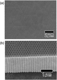
Fig. 2a shows a surface SEM image of the porous alumina mask used for the dry etching of a Ti substrate. The SEM image shows that uniformly sized holes were ideally arranged over the sample. The hole period of the porous alumina mask was 200 nm. Fig. 2b shows a surface SEM image of the Ti substrate after Ar ion milling. The SEM image reveals that an ordered concave array was formed by Ar ion milling using a porous alumina mask. The period of the concave array formed on the surface of the Ti substrate was 200 nm, in good agreement with the hole period of the porous alumina mask. The average depth of each concave pit was 20 nm, which was determined by atomic force microscopy.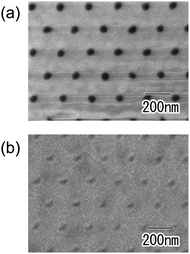 | ||
| Fig. 2 (a) Surface SEM image of the porous alumina mask with a 200 nm-period ideally ordered hole arrangement. (b) Surface SEM image of Ti substrate after pre-patterning by Ar ion milling. | ||
Fig. 3 shows SEM images of ideally ordered porous TiO2 obtained by anodization. From the surface image shown in Fig. 3a, it can be seen that an ideally ordered hole array structure was obtained by the anodization of the pre-patterned Ti substrate. This result means that each concave pit formed by Ar ion milling acted as an initiation site for hole development during anodization. The cross-sectional image (Fig. 3b) shows that a hexagonal cell with a cylindrical hole at its center grew straight in the depth direction. This result indicates that the ideally ordered hole arrangement formed at the surface of the sample was maintained in the depth direction.
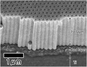
Fig. 4 shows a cross-sectional SEM image of the sample after heat treatment and subsequent second anodization. After the heat treatment, the crystalline phase of the TiO2 layer was changed from amorphas to anatase. In this SEM image, the oxide layer formed by the second anodization was observed at the lower part of the heat-treated oxide layer. During the second anodization, the growth of an oxide layer started after a leading time; because the solubility of the heat-treated oxide layer was low, it took time for the anodic oxidation reaction to proceed. The thickness of the oxide layer formed by the second anodization can be better controlled by adjusting the anodic charge rather than the anodization time.
Fig. 5 shows SEM images of the ideally ordered TiO2 through-hole membrane obtained by the selective dissolution of the oxide layer formed by the second anodization. The top surface (Fig. 5a) and back surface (Fig. 5b) images show that ideally ordered through-holes were arranged hexagonally over the sample. The hole period at both surfaces was 200 nm. The size of the ideally ordered TiO2 through-hole membrane depends on that of the porous alumina mask used for the pretexturing of Ti. In this study, the samples with 5 × 5 mm2 in size were obtained. The thickness of the membrane was 3.5 μm, as shown in Fig. 5c. The thickness of the membranes can be controlled by adjusting the anodization time. In this study, TiO2 through-hole membranes with a film thickness of 1 to 5 μm were obtained. The mechanical strength of the obtained TiO2 membrane was low because the film thickness was thin. We think that the introduction of support filters is an effective way to ensure mechanical strength.
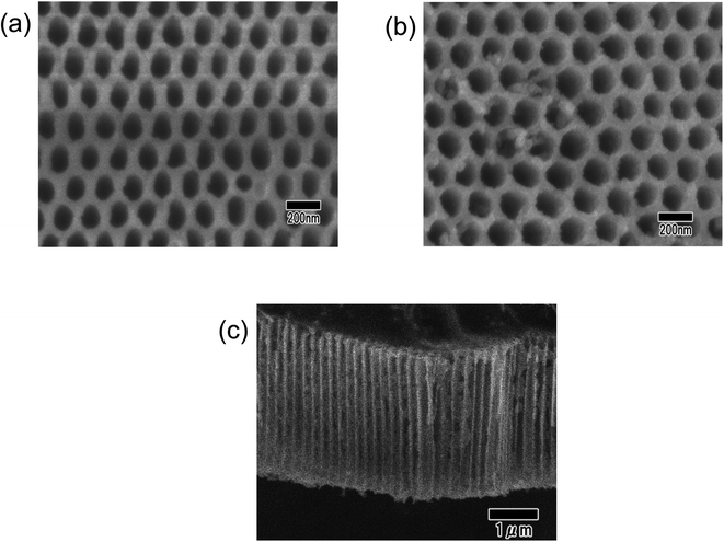 | ||
| Fig. 5 SEM images of ideally ordered TiO2 through-hole membrane: (a) top surface, (b) back surface, and (c) cross-sectional views. | ||
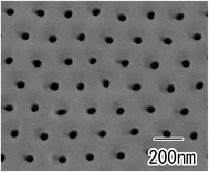
In the present process, the ideally ordered concave arrays were maintained at the surface of the residual Ti substrate after the detachment of the membrane. Therefore, ideally ordered porous TiO2 was successfully prepared by the subsequent anodization of residual Ti. Fig. 6 shows a surface SEM image of the sample obtained by the anodization of the residual Ti substrate after the detachment of the membrane. From the SEM image, it can be seen that ideally ordered porous TiO2 was formed by the subsequent anodization. In addition, an ideally ordered TiO2 through-hole membrane was also obtained by the two-layer anodization. This indicates that the present process enables the repeated preparation of ideally ordered TiO2 through-hole membranes from a single Ti substrate by the repetition of this process.
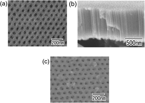
The hole period of anodic porous TiO2 can be controlled by changing the anodizing voltage. Fig. 7a and b show SEM images of the ideally ordered TiO2 through-hole membrane with a hole period of 100 nm. For this sample, the anodization of the Ti substrate with a 100 nm-period concave array was carried out under a constant voltage of 40 V in an ethylene glycol electrolyte containing 0.38 wt% NH4F and 1 wt% H2O at 20 °C. The top surface (Fig. 7a) and cross-sectional (Fig. 7b) images revealed that an ideally ordered through-hole membrane was prepared even in the case of a hole period of 100 nm. Fig. 7c shows a surface SEM image of the sample obtained by the subsequent anodization of the residual Ti after detaching the TiO2 membrane. As shown in Fig. 7c, an ideally ordered hole arrangement with a hole period of 100 nm was successfully obtained by the subsequent anodization. From this result, we concluded that the present process is effective for the high-throughput preparation of ideally ordered TiO2 membranes with a controlled hole period.
Conclusions
Ideally ordered TiO2 through-hole membranes with a hole period of 200 nm were formed by a combination of Ti substrate pre-patterning and two-layer anodization. This process allows the efficient preparation of ideally ordered TiO2 through-hole membranes. The residual Ti substrate can be used for the repeated preparation of ideally ordered TiO2 membranes because the ordered concave array corresponding to the hole arrangement of the detached membrane was maintained even after detaching the TiO2 membrane. The hole period of the ideally ordered TiO2 through-hole membrane can also be controlled by adjusting the preparation conditions. The present process enables the repeated high-throughput preparation of ideally ordered TiO2 through-hole membranes with a controlled hole period. The obtained samples are expected to be used for various optical devices requiring an ideally ordered hole arrangement, such as photonic crystals and optical waveguides.Conflicts of interest
There are no conflicts to declare.Acknowledgements
This research was supported by the Light Metal Educational Foundation and JSPS KAKENHI (20K05171).References
- P. Roy, S. Berger and P. Schmuki, Angew. Chem., Int. Ed., 2011, 50, 2904 CrossRef CAS.
- K. Lee, A. Mazare and P. Schmuki, Chem. Rev., 2014, 114, 9385 CrossRef CAS.
- J. M. Macák, H. Tsuchiya, A. Ghicov and P. Schmuki, Electrochem. Commun., 2005, 7, 1133 CrossRef.
- H. Tiainen, J. C. Wohlfahrt, A. Verket, S. P. Lyngstadaas and H. J. Haugen, Acta Biomater., 2012, 8, 2384 CrossRef CAS.
- Y. K. Lai, L. Sun, C. Chen, C. G. Nie, J. Zuo and C. J. Lin, Appl. Surf. Sci., 2005, 252, 1101 CrossRef CAS.
- H. Liv, N. Li, H. Zhang, Y. Tian, H. Zhang, X. Zhang, H. Qu, C. Liu, C. Jia, J. Zhao and Y. Li, Sol. Energy Mater. Sol. Cells, 2016, 150, 57 CrossRef.
- S. Mohajernia, A. Mazare, E. Gongadze, V. Kralj-iglič, A. Iglič and P. Schmuki, Electrochim. Acta, 2017, 245, 25 CrossRef CAS.
- S. Noothonbkaew, O. Thumthan and K. An, Mater. Lett., 2018, 218, 274 CrossRef.
- H. Lv, N. Li, H. Zhang, Y. Tian, H. Zhang, X. Zhang, H. Qu, C. Liu, C. Jia, J. Zhao and Y. Li, Sol. Energy Mater. Sol. Cells, 2016, 150, 57 CrossRef CAS.
- A. F. Gualdrón-Reyes, A. Cárdenas-Arenas, C. A. Martínez, V. V. Kouznetsov and A. M. Meléndez, J. Phys. Conf., 2017, 766, 012044 CrossRef.
- K. Lee and S. A. Asher, J. Am. Chem. Soc., 2000, 122, 9535 Search PubMed.
- D. Englund, D. Fattal, E. Waks, G. Solomon, B. Zhang, T. Nakaoka, Y. Arakawa, Y. Yamamoto and J. Vuckovic, Phys. Rev. Lett., 2005, 95, 013904 CrossRef.
- T. Kondo, S. Nagao, T. Yanagishita, N. T. Nguyen, K. Lee, P. Schmuki and H. Masuda, Electrochem. Commun., 2015, 50, 73 CrossRef CAS.
- T. Kondo, A. Nagao, T. Yanagishita and H. Masuda, J. Electrochem. Soc., 2016, 163, E206 CrossRef CAS.
- T. Yanagishita, H. Inada, T. Kondo, N. T. Nguyen, P. Schmuki and H. Masuda, J. Electrochem. Soc., 2018, 165, E763 CrossRef CAS.
| This journal is © The Royal Society of Chemistry 2020 |

