
Electron–phonon interaction in In-induced  structures on Si(111) from first-principles

Irina Yu.
Sklyadneva
 *abc,
Rolf
Heid
b,
Pedro
M. Echenique
ade and
Eugene V.
Chulkov
acdef
*abc,
Rolf
Heid
b,
Pedro
M. Echenique
ade and
Eugene V.
Chulkov
acdef
aDonostia International Physics Center (DIPC), 20018 San Sebastián/Donostia, Basque Country, Spain
bInstitute for Quantum Materials and Technologies, Karlsruhe Institute of Technology, 76021 Karlsruhe, Germany
cTomsk State University, 634050, Tomsk, Russian Federation
dDepartamento de Física de Materiales, Facultad de Sciencias Químicas UPV/EHU, Apdo. 1072, 20080 San Sebastián/Donostia, Basque Country, Spain
eCentro de Física de Materiales CFM – Materials Physics Center MPC, Centro Mixto CSIC-UPV/EHU, 20018, San Sebastián/Donostia, Basque Country, Spain
fSt. Petersburg State University, 199034, St. Petersburg, Russian Federation
First published on 5th January 2021
Abstract
Electron–phonon interaction in the Si(111)-supported rectangular  phases of In is investigated within the density-functional theory and linear-response. For both single-layer and double-layer
  structures, it is found that the phonon-induced scattering of electrons is almost exclusively determined by vibrations of In atoms. It is shown that the strength of electron–phonon coupling at the Fermi level λ(EF) increases almost twofold upon adding the second In layer. One of the reasons is that additional low-frequency modes appear in the phonon spectrum, which favors a strong enhancement of λ(EF). The agreement of the calculated parameter λ(EF) = 0.99 for a double-layer structure as well as the superconducting transition temperature Tc = 3.5 K with experimental estimates indicates that the discovered superconducting phase is probably a double-layer rectangular
  -In structure on Si(111) with a coverage of 2.4 ML. This conclusion is also supported by good agreement between the calculated electron band structure and ARPES measurements.
Introduction
Along with advances in nanotechnology, low-dimensional materials have attracted much attention due to their two-dimensional (2D) physical properties.1–7 An important class of such 2D systems is formed by ultrathin metal films grown on semiconductor substrates, which are especially interesting because of the discovered two-dimensional superconductivity.8–18 Among them, various structures of indium on a silicon substrate, in particular, on Si(111) with lateral periodicity,19–23 forming a well-defined nonreactive interface,24 have been intensively studied experimentally.14–17,25–27
The rectangular  phase exhibits 2D electronic features with metallic transport properties down to several Kelvin.25,26 In the angle-resolved photoemission spectroscopy (ARPES) study,25 not only the band structure of the metallic phase was clarified, but also the electron–phonon (e–ph) coupling parameter was roughly estimated from the temperature-dependent photoemission spectra. The obtained unusually high value of λ ∼ 1 is very close to the e–ph coupling parameter in bulk In. Later, scanning tunnelling spectroscopy (STS) measurements14 showed that the Si(111)-
 -In surface becomes superconducting at about 3.18 K, which is close to the bulk value of Tc = 3.4 K.
The discovery of superconductivity was followed by the demonstration of macroscopic superconducting currents on the Si(111)- -In surface.15 The transition temperature determined from measurements of direct electron transport15 and conductivity,16Tc = 2.8 K, turned out to be slightly lower than the value obtained from the opening of a superconducting energy gap.14 Further study of electron transport on the Si(111)-
 -In surface28 confirmed that Tc is in the range from 2.64 to 2.99 K, which is consistent with previously determined values.14,15
As for the e–ph coupling parameter, it was estimated25 not only at the Fermi level (EF), but was also obtained for several 2D metallic states on the Si(111)- -In surface from the temperature dependence of the surface state energy width.17 The extracted λ's vary from 0.8 to 1.0 and are close to the value for bulk indium, λ = 0.9 ± 0.1.29
It is known that there are two different  structures of In on Si(111), hexagonal and rectangular. Both phases coexist19 and can be topographically distinguished in scanning tunnelling microscopy (STM) experiments.19,20 The rectangular structure is thermodynamically stable,30 while the hexagonal phase has been shown to be metastable.27 The metallic behavior25,26 and the superconducting gap14 were observed precisely in the rectangular
  phase.
An important question concerns the number of In layers that form the  structure on the silicon surface, i.e. whether it consists of a single layer of In atoms or contains several layers. It was initially assumed that this phase is one atomic layer thick (1.2 ML).19,20,31 However, further density-functional theory (DFT) calculations30,32,33 as well as X-ray photoemission spectroscopy33 showed that the rectangular
  phase represents a double-layer (2.4 ML) In film on Si(111) while the hexagonal
  structure corresponds to a coverage of 1.2 ML.34 It was found that the double-layer In film is energetically more favourable and reproduces the measured photoemission band structure well, in contrast to the single-layer model.30,34 Recently, a quantitative analysis of X-ray and low-energy electron diffraction (LEED) spectra verified the double-layer model of
  -In with a rectangular arrangement.35
Although extensive studies have been carried out on the superconductivity of In films on Si(111) using various experimental tools, an accurate quantitative description and analysis of the e–ph coupling in the Si(111)-supported  -In films is still lacking. Therefore, it seems useful to study the e–ph interaction, as well as analyze how the e–ph coupling changes when another In layer is added. This is especially important in connection with the question of the number of In layers that form the
  structure on the Si(111) surface.
Here we present the results of a first-principles study of the lattice dynamics and the pairing strength in the e–ph scattering processes for both single-layer and double-layer  -In structures on Si(111). First of all, we calculated the e–ph coupling constant and Eliashberg spectral function, averaged over electron momentum at the Fermi energy. Then, the superconducting transition temperature was estimated by solving the linearized gap equation. We also analyze the state-dependent strength of e–ph interaction in several In electronic bands.
Calculation details
Method
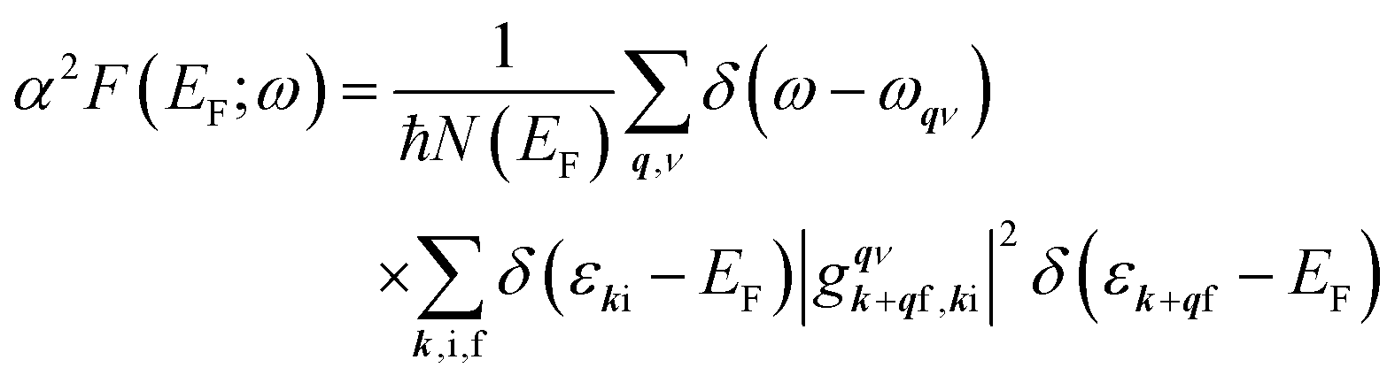
The strength of electron–phonon interaction averaged over electron momentum at EF is defined as36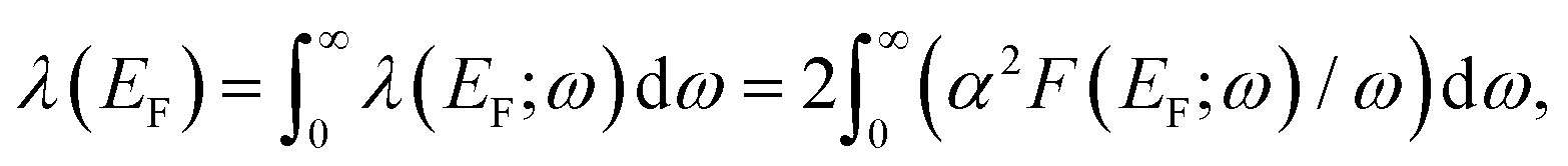 | (1) |
is the Eliashberg spectral function. Here gqνk+gf,ki is the e–ph matrix element, εki and εk+qf are energies of initial (i) and final (f) electronic states, and N(EF) is the density of electronic states. The summation is carried out over all combinations of electronic states (ki) and (k + qf) and phonon modes (qν). The calculation of λ(EF) is difficult because of the slow convergence of the sum over (ki). Therefore, it is more convenient to use a rather coarse but suitable k-point grid37 for calculating phonons and a dense k-point mesh for summation over electronic states at the Fermi level. In our study, for averaging the e–ph parameter over electron momentum, we used a (48 × 48 × 1) k-point grid corresponding to 601 special points in the irreducible part of the surface Brillouin zone (SBZ).
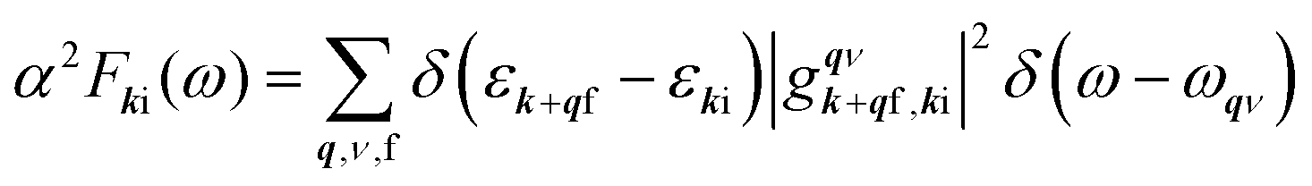
To calculate the e–ph coupling parameter for a specific electronic state with momentum k and band index i, λki, the corresponding state-dependent Eliashberg spectral function is used:
All calculations were carried out within the density-functional formalism and the local density approximation38 in the mixed-basis approach.39–41 The scheme employs a combination of local functions and plane waves to represent valence states.39,40 The norm-conserving pseudopotentials were constructed according to the scheme proposed by Vanderbilt,42 with the inclusion of indium semicore 4d states in the valence shell for greater accuracy. By using d-type local functions at each atomic site of In, the cutoff energy for plane waves can be reduced to 20 Ry without loss of accuracy. Dynamical properties were calculated using the linear response technique.43 Integrations over the SBZ in the self-consistent calculations were performed by sampling a uniform (12 × 12 × 1) k-point mesh37 corresponding to 43 points in the irreducible part of SBZ, in combination with a Gaussian broadening with a smearing parameter of 0.05 eV.
Since e–ph matrix elements for a fixed electronic state display rather significant variations throughout the SBZ, the sum over wave vectors requires a dense mesh of q-points. So, we first calculated the e–ph matrices using a 12 × 12 × 1 q-point grid. Then, to check the convergence, we used a denser 48 × 48 × 1 q-point mesh. For the additional q vectors, the matrix elements were calculated using a Fourier interpolation scheme for the change of the self-consistent potential with respect to atomic displacements as well as for the dynamical matrices. The difference in λki's, obtained on the two grids, does not exceed 0.04.
Structural parameters
The silicon substrate is modelled by periodically repeating two Si(111) bilayers separated by a vacuum gap of ∼12 Å. The lattice constant is first fixed at the theoretical bulk Si lattice parameter a = 5.402 Å obtained by total-energy minimization which is a bit smaller than the experimental value,44aexp = 5.43 Å. Indium atoms are then deposited on top of the substrate according to the atomic arrangement proposed for single-layer19 and double-layer30 -In rectangular phases on Si(111) (see Fig. 1). The silicon dangling bonds at the bottom of the slab are saturated with hydrogen atoms.
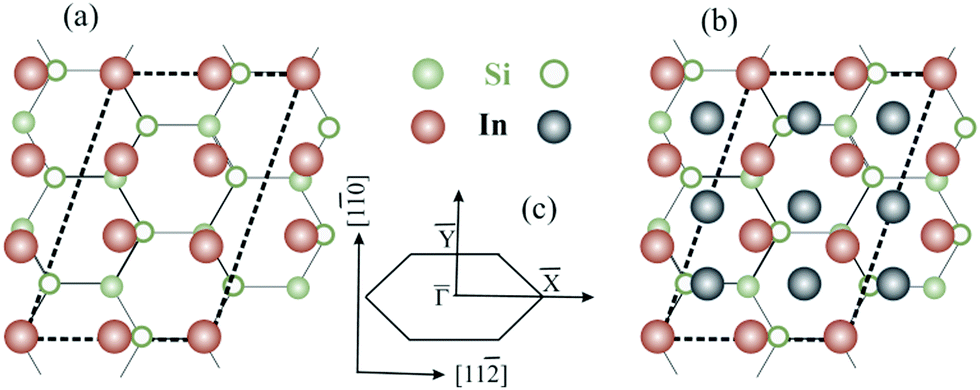 | ||
Fig. 1 (a and b) Top view of (a) the single-layer19 and (b) the double-layer30 rectangular models for  -In structure on Si(111). Big circles correspond to In atoms. Si atoms are shown by full (in the first substrate layer) and open (in the second layer) small circles. The colour assignments are as follows: brown (grey), In atoms in the interface (top) layer; green, Si atoms of the substrate. The dashed line indicates the -In structure on Si(111). Big circles correspond to In atoms. Si atoms are shown by full (in the first substrate layer) and open (in the second layer) small circles. The colour assignments are as follows: brown (grey), In atoms in the interface (top) layer; green, Si atoms of the substrate. The dashed line indicates the  unit cell. (c) The surface Brillouin zones of the unit cell. (c) The surface Brillouin zones of the  unit cell. unit cell. | ||
The bottom Si atoms and hydrogen are held fixed to simulate the bulk environment. The H–Si distance was obtained in the calculation for a Si(111) film saturated with H on both sides. All other atoms are allowed to move both in-plane and along the stacking direction until the forces are less than 0.025 eV Å−1. Some optimized structural parameter are given in Tables 1 and 2 together with available data from other first-principles calculations30,33 and experiments.19,34
 -In on Si(111): lateral distances (in Å) between In atoms, dIn–In{xy}, and the height difference between atoms at the interface, ΔzIn–Si. For Δz both maximum (max) and averaged (av) values are given
| Present calc. | STM19 | ||
|---|---|---|---|
| d In–In{xy} | [1![[1 with combining macron]](https://www.rsc.org/images/entities/char_0031_0304.gif) 0] 0] |
3.18 | 3.2 |
[11![[2 with combining macron]](https://www.rsc.org/images/entities/char_0032_0304.gif) ] ] |
3.27 | 3.326 | |
| ΔzIn–Si | (max) | 2.67 | 2.8 |
| (av) | 2.55 | ||
 -In on Si(111): lateral distances (in Å) between In atoms in the top and subsurface layers, dIn–In{xy}. The height difference is given both for atoms at the interface, ΔzIn–Si, and between In layers, ΔzIn–In
The single-layer  unit cell contains six In atoms. With this coverage, equivalent to 1.2 ML, the atomic density in the adlayer is almost the same as in the bulk In(001) layer. The In atoms are arranged in a slightly distorted close-packed rectangular lattice. They are not equivalent with respect to the underlying substrate: only two of them are located exactly above the Si atoms from the upper layer. As a consequence, the adlayer appears slightly buckled; the calculated average value of 0.2 Å is close to the buckling obtained in the STM experiment, 0.25 Å.19
In the double-layer model,30 the second-layer In atoms were initially located at the hollow sites of the first quasi-rectangular In layer like in the case of the In(001) surface. The optimized In–In interlayer spacing, on average, 2.40 Å, is slightly shorter than the interlayer distance for the In(001) surface, 2.47 Å. The interface spacing practically does not change when the second In layer is added. The calculated averaged buckling in the top In layer, 0.014 Å, is substantially smaller than the value obtained for the single-layer  structure.
Results and discussion
Fig. 2(a and b) show the calculated band structure for both the initially proposed single-layer and double-layer models, together with the experimental ARPES data.25 The calculated and measured Fermi levels coincide in the figures. The SBZ symmetry points are given in Fig. 1(c). As one can see in both cases the band structure has a metallic character with several bands crossing EF. A detailed description of the band spectra can be found in ref. 30 and 34, where it was reported that the double-layer In structure reproduces the experimental dispersions much better than the single-layer -In model. The calculated energy bands for a single
  -In layer on Si(111) are qualitatively different from the ARPES experimental data for the rectangular structure.25
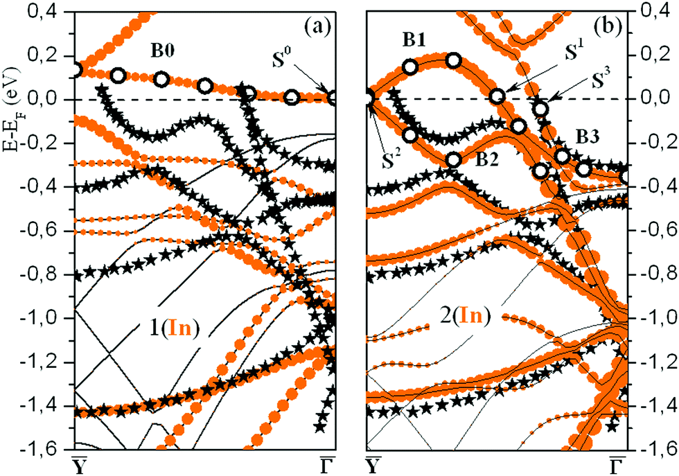 | ||
Fig. 2 (a and b) Calculated band structure of the  rectangular phase for (a) 1.2 ML and (b) 2.4 ML of In on Si(111). Filled (orange) circles show electronic bands formed mainly by In orbitals. The In electronic states, for which the e–ph coupling strength is calculated, are marked by open circles. Stars represent the ARPES bands reported in ref. 25. rectangular phase for (a) 1.2 ML and (b) 2.4 ML of In on Si(111). Filled (orange) circles show electronic bands formed mainly by In orbitals. The In electronic states, for which the e–ph coupling strength is calculated, are marked by open circles. Stars represent the ARPES bands reported in ref. 25. | ||
First, we estimated the momentum-averaged e–ph interaction at the Fermi level of both structures. The calculated values for a single-layer, λ1(In)(EF) = 0.46, and double-layer  -In structures on Si(111), λ2(In)(EF) = 0.99, show that the strength of e–ph coupling becomes two times larger when a second In layer is added. The value of λ(EF) for the double-layer model is consistent with the e–ph coupling strength estimated in the variable-temperature ARPES measurements,25λ ∼ 1, and slightly less than the e–ph coupling constant obtained from the analysis of the transport properties of the Si-
 -In surface, λ(EF) = 1.2.26 This value is also close to the bulk indium parameter, λ(EF) = 0.9 ± 0.1.29
One of the factors determining λ is the phase space, that is, the number of electronic states available for scattering processes. However, the density of electronic states at the Fermi level in these structures, N(EF), is practically the same; the difference is only 5%.
Another factor is related to lattice vibrations and e–ph matrix elements. The calculated phonon density of states for both  -In structures on Si(111) is presented in Fig. 3(a and b). The phonons associated with displacements of In atoms lie below 14 meV, while vibrations of the substrate atoms occupy the high-frequency region up to 72 meV. The most significant difference is that when a second In layer is added, additional modes appear in the phonon spectrum associated with the motion of adatoms. The arising low-frequency vibrations lie below the edge of the phonon spectrum for the single-layer case, thereby contributing to a significant increase in λ(EF).
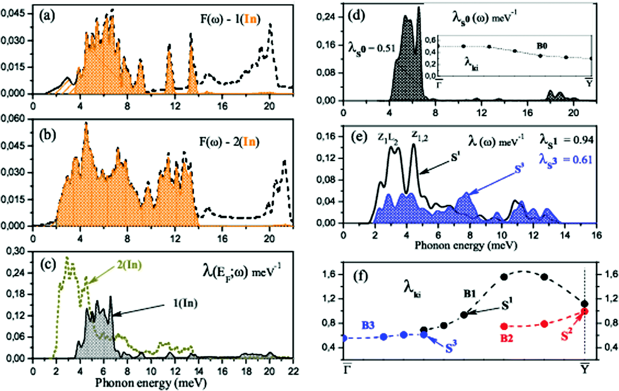 | ||
| Fig. 3 (a and b) Phonon density of states F(ω) for (a) 1.2 ML and (b) 2.4 ML of In on Si(111). Hatched areas show the contribution of In-localized modes. (c) Spectral decomposition of the e–ph coupling parameter at the Fermi level, λ(EF;ω) for both structures. (d and e) Spectral decomposition of λki, for electronic states (d) S0, (e) S1 and S3 (see Fig. 2(a and b)). The inset in (d) gives the momentum dependence of λki for electronic states in the B0 band. (f) The momentum dependence of λki for electronic states marked by open circles in Fig. 2(b). | ||
From the spectral decomposition of λ(EF)'s shown in Fig. 3(c), it is obvious that for both structures the phonon-mediated scattering of electrons is actually determined by the vibrations of In adatoms. The substrate-localized modes involved in the e–ph coupling are high-frequency vibrations, and λ scales approximately as 1/ω2.
In the case of a single  -In layer on Si(111), all bands near the Fermi level are, in a varying degree, a hybridization of In orbitals with Si states from the topmost valence band, which indicates a considerable effect of the substrate on the formation of quantum well states in the one-atom thick adlayer. The electronic bands that provide λ(EF) are formed by In states of either s, pz or px character coupled to pz orbitals of atoms from the substrate surface layer (dangling bonds).
Another feature of the single-layer  structure on Si(111) is that the contributions to λ(EF) from vibrations of different In atoms are not identical, but strongly depend on the position of the adatom relative to the underlying Si surface layer. The e–ph interaction is actually determined by the vibrations of the In atoms, which are located in the top (or nearly top) sites of the Si(111) surface and form a covalent bond with an underlying substrate atom.
Besides the e–ph coupling parameter averaged over the electron momentum at the Fermi level, we also analyzed phonon-mediated transitions for some specific electronic states in the band crossing EF near the SBZ center (B0). The states are marked by open circles in Fig. 2(a). The obtained spectral function λki(ω) for state S0 is shown in Fig. 3(d) as a typical example. Obviously, the modes that determine the e–ph coupling are shear-vertical (perpendicular to the surface) vibrations of In atoms (4–7 meV). The contribution of optical modes characterized by the in-plane motion of In and substrate atoms is almost completely suppressed. This is largely due to the orbital composition of this electron band, with the prevalence of pz orbitals of both In and Si at the interface. Thus, the overwhelming contribution is made by the states that determine the adhesion of the adlayer and the substrate. The λki's for all states marked with open circles are shown in the inset of Fig. 3(d). As can be seen, the strength of e–ph interaction varies between 0.3 and 0.5. The value λS0 = 0.51 is a bit larger than the e–ph parameter averaged over electron momentum, λ1(In)(EF) = 0.46.
When a second In layer is added, all bands around the Fermi level are entirely composed of In orbitals. The In-induced electronic states that prevail in the e–ph scattering are of s, px(y) (or s, pz) type in the top layer and take on a px character in the second layer. Thus, it is the states that are responsible for the metallic in-plane bonding in the adlayers that determine the e–ph scattering. Unlike the single-layer  structure, the contributions to λ(EF) from vibrations of different In atoms are the same, regardless of the layer and the position of the adatom in the layer.
We also calculated the e–ph coupling parameters for a number of electronic states in the  symmetry direction, marked with open circles in Fig. 2(b). The obtained λki's are shown in Fig. 3(f), and the spectral functions λki(ω) for two states, S1 and S3, are given in Fig. 3(e). The strength of electron–phonon interaction for several specific electronic states has also been previously estimated experimentally by Uhm et al. in ref. 17.
S1 is a state of s, px character and is mostly localized in the top In layer, while the S2 state is largely derived from the in-plane In–In bonding at the interface. The spectral function (see Fig. 3(e)), reveals that modes characterized by vertical displacements of In atoms still play an important role in the e–ph scattering, but, unlike a single-layer structure, the contribution of longitudinal plane vibrations of adatoms becomes noticeable. The calculated e–ph coupling parameters, λS1 = 0.94 and λS2 ∼ 1, are very close to the values (0.8–1.0), extracted from the slope of the temperature-depended linewidth.17
All states in the B3 band are localized in both In layers and consist predominantly of orbitals of the s, py-type. However, when approaching the SBZ center, a hybridization of In orbitals with Si states from the topmost valence band increases. The strength of e–ph coupling in the B3 band is generally moderate and ranges from 0.5 to 0.6 (λS3 = 0.61). The corresponding spectral function shows that the contribution of low-energy (mainly shear-vertical) vibrations of In atoms is significantly reduced. This suppression of the lower-energy motion of adatoms contributes to a decrease in lambda by almost a factor of two.
For the rectangular  phase of In on the Si(111) surface, STS measurements14 demonstrated a transition to the superconducting phase at Tc = 3.18 K, while the conductivity measurements15,16 showed Tc = 2.8 K. We have estimated Tc by solving the linearized gap equation of the Eliashberg theory45 with a standard value of 0.1 for the Coulomb pseudopotential μ*. For a single-layer structure, as expected, the calculated temperature is very low, Tc ∼ 0.6 K due to the small value of λ(EF). For a double-layer structure, the estimation of the superconducting transition temperature gave Tc = 3.5 K in a good agreement with the experimental value14 of 3.18 K and close to Tc = 3.4 K for bulk In. Thus, it is most likely that the superconducting phase is a double-layer rectangular In structure on Si(111) with a coverage of 2.4 ML.
Conclusions
We have presented the results of a first-principles study of the electron–phonon coupling in the single-layer and double-layer -In rectangular structures on Si(111). The obtained values λ1(In)(EF) = 0.46 and λ2(In)(EF) = 0.99 show a significant difference in the phonon-mediated transitions of electrons in the two structures.
It was found that, in both cases, the scattering of electrons is controlled by vibrations of In atoms. The phase space available for scattering processes at the Fermi level is practically the same in both cases, but this does not apply to the lattice dynamics. In the case of a double In layer, additional low-frequency vibrations arise, which contributes to a significant increase in the e–ph coupling strength as compared to a single-layer structure, where λ1(In)(EF) is almost two times less than the value observed experimentally. Not only λ2(In)(EF), but also the calculated superconducting transition temperature Tc = 3.5 K indicate that the observed experimentally superconducting phase14 is probably a double-layer rectangular  In structure on Si(111) with a coverage of 2.4 ML.
Conflicts of interest
There are no conflicts to declare.Acknowledgements
This work has been supported by the University of the Basque Country (Grants No. GIC07-IT-366-07 and IT-756-13), the Spanish Ministry of Science and Innovation (Grant No. FIS2016-75862-P), the Tomsk State University competitiveness improvement program (Grant No. 8.1.01.2018) and Saint Petersburg State University (ID 51126254). The authors acknowledge support by the state of Baden-Württemberg through bwHPC.References
- C. Corriol, V. M. Silkin, D. Sánchez-Portal, A. Arnau, E. V. Chulkov, P. M. Echenique, T. von Hofe, J. Kliewer, J. Kröger and R. Berndt, Phys. Rev. Lett., 2005, 95, 176802 CrossRef CAS.
- P. S. Kirchmann and U. Bovensiepen, Phys. Rev. B: Condens. Matter Mater. Phys., 2008, 78, 035437 CrossRef.
- A. B. Schmidt, M. Pickel, M. Donath, P. Buczek, A. Ernst, V. P. Zhukov, P. M. Echenique, L. M. Sandratskii, E. V. Chulkov and M. Weinelt, Phys. Rev. Lett., 2010, 105, 197401 CrossRef CAS.
- S. Kim, S. C. Jung, M. H. Kang and H. W. Yeom, Phys. Rev. Lett., 2019, 104, 246803 CrossRef.
- G. Benedek, M. Bernasconi, K.-P. Bohnen, D. Campi, E. V. Chulkov, P. M. Echenique, R. Heid, I. Yu. Sklyadneva and J. P. Toennies, Phys. Chem. Chem. Phys., 2014, 16, 7159 RSC.
- G. G. Rusina, S. D. Borisova, S. V. Eremeev, I. Yu. Sklyadneva, E. V. Chulkov, G. Benedek and J. P. Toennies, J. Phys. Chem. C, 2016, 120, 22304 CrossRef CAS.
- I. Yu. Sklyadneva, G. Benedek, R. Heid, P. M. Echenique, J. P. Toennies and E. V. Chulkov, J. Phys. Chem. C, 2018, 122, 29039 CrossRef CAS.
- T. Nishio, T. An, A. Nomura, K. Miyachi, T. Eguchi, H. Sakata, S. Lin, N. Hayashi, N. Nakai, M. Machida and Y. Hasegawa, Phys. Rev. Lett., 2008, 101, 167001 CrossRef.
- S. Y. Qin, J. Kim, Q. Niu and C. K. Shih, Science, 2009, 324, 1314 CrossRef CAS.
- C. Brun, I. P. Hong, F. Patthey, I. Yu. Sklyadneva, R. Heid, P. M. Echenique, K.-P. Bohnen, E. V. Chulkov and W. D. Schneider, Phys. Rev. Lett., 2009, 102, 207002 CrossRef.
- H.-M. Zhang, Y. Sun, W. Li, J.-P. Peng, C.-L. Song, Y. Xing, Q. Zhang, J. Guan, Z. Li, Y. Zhao, S. Ji, L. Wang, K. He, X. Chen, L. Gu, L. Ling, M. Tian, L. Li, X. C. Xie, J. Liu, H. Yang, Q.-K. Xue, J. Wang and X. Ma, Phys. Rev. Lett., 2015, 114, 107003 CrossRef.
- A. V. Matetskiy, S. Ichinokura, L. V. Bondarenko, A. Y. Tupchaya, D. V. Gruznev, A. V. Zotov, A. A. Saranin, R. Hobara, A. Takayama and S. Hasegawa, Phys. Rev. Lett., 2015, 115, 147003 CrossRef CAS.
- S. Ichinokura, L. V. Bondarenko, A. Y. Tupchaya, D. V. Gruznev, A. V. Zotov, A. A. Saranin and S. Hasegawa, 2D Mater., 2017, 4, 025020 CrossRef.
- T. Zhang, P. Cheng, W. J. Li, Yu.-J. Sun, G. Wang, X. G. Zhu, K. He, L. Wang, X. Ma, X. Chen, Y. Wang, Y. Liu, H. Q. Lin, L. F. Jia and Q. K. Xue, Nat. Phys., 2010, 6, 104 Search PubMed.
- T. Uchihashi, P. Mishra, M. Aono and T. Nakayama, Phys. Rev. Lett., 2011, 107, 207001 CrossRef.
- M. Yamada, T. Hirahara and S. Hasegawa, Phys. Rev. Lett., 2013, 110, 237001 CrossRef.
- S. H. Uhm and H. W. Yeom, Phys. Rev. B: Condens. Matter Mater. Phys., 2012, 86, 245408 CrossRef.
- S. Yoshizawa, H. Kim, T. Kawakami, Y. Nagai, T. Nakayama, X. Hu, Y. Hasegawa and T. Uchihashi, Phys. Rev. Lett., 2014, 113, 247004 CrossRef.
- J. Kraft, S. Surnev and F. P. Netzer, Surf. Sci., 1995, 340, 36 CrossRef CAS.
- J. Kraft, M. G. Ramsey and F. P. Netzer, Phys. Rev. B: Condens. Matter Mater. Phys., 1997, 55, 5384 CrossRef CAS.
- C. González, F. Flores and J. Ortega, Phys. Rev. Lett., 2006, 96, 136101 CrossRef.
- K. Iwata, S. Yamazaki, Y. Tani and Y. Sugimoto, Appl. Phys. Express, 2013, 6, 055202 Search PubMed.
- S. Terakawa, S. Hatta, H. Okuyama and T. Aruga, J. Phys.: Condens. Matter, 2018, 30, 365002 CrossRef.
- H. Öfner, S. L. Surnev, Y. Shapira and F. P. Netzer, Phys. Rev. B: Condens. Matter Mater. Phys., 1993, 48, 10940 CrossRef.
- E. Rotenberg, H. Koh, K. Rossnagel, H. W. Yeom, J. Schafer, B. Krenzer, M. P. Rocha and S. D. Kevan, Phys. Rev. Lett., 2003, 91, 246404 CrossRef.
- S. Yamazaki, Y. Hosomura, I. Matsuda, R. Hobara, T. Eguchi, Y. Hasegawa and S. Hasegawa, Phys. Rev. Lett., 2011, 106, 116802 CrossRef.
- A. A. Saranin, A. V. Zotov, M. Kishida, Y. Murata, S. Honda, M. Katayama, K. Oura, D. V. Gruznev, A. Visikovskiy and H. Tochihara, Phys. Rev. B: Condens. Matter Mater. Phys., 2006, 74, 035436 CrossRef.
- T. Uchihashi, P. Mishra and T. Nakayama, Nanoscale Res. Lett., 2013, 8, 167 CrossRef.
- S. P. Rudin, R. Bauer, A. Y. Liu and J. K. Freericks, Phys. Rev. B: Condens. Matter Mater. Phys., 1998, 58, 14511 CrossRef CAS.
- J. W. Park and M. H. Kang, Phys. Rev. Lett., 2012, 109, 166102 CrossRef.
- B. Shang, L.-F. Yuan and J.-l. Yang, Chin. J. Chem. Phys., 2012, 25, 403 CrossRef CAS.
- J. W. Park and M. H. Kang, Phys. Rev. B: Condens. Matter Mater. Phys., 2015, 92, 045306 CrossRef.
- T. Suzuki, J. Lawrence, M. Walker, J. M. Morbec, P. Blowey, K. Yagyu, P. Kratzer and G. Costantini, Phys. Rev. B, 2017, 96, 035412 CrossRef.
- K. Uchida and A. Oshiyama, Phys. Rev. B: Condens. Matter Mater. Phys., 2013, 87, 165433 CrossRef.
- T. Shirasawa, S. Yoshizawa, T. Takahashi and T. Uchihashi, Phys. Rev. B, 2019, 99, 100502(R) CrossRef.
- P. B. Allen and M. L. Cohen, Phys. Rev., 1969, 187, 525 CrossRef CAS.
- H. J. Monkhorst and J. D. Pack, Phys. Rev. B: Solid State, 1976, 13, 5188 CrossRef.
- L. Hedin and B. I. Lundqwist, J. Phys. C: Solid State Phys., 1971, 4, 2064 CrossRef.
- S. G. Louie, K. M. Ho and M. L. Cohen, Phys. Rev. B: Condens. Matter Mater. Phys., 1979, 19, 1774 CrossRef CAS.
- B. Meyer, C. Elsässer, F. Lechermann and M. Fähnle, FORTRAN90, Program for Mixed-Basis-Pseudopotential Calculations for Crystals, Max-Planck-Institut für Metallforschung, Stuttgart Search PubMed.
- R. Heid and K.-P. Bohnen, Phys. Rev. B: Condens. Matter Mater. Phys., 1999, 60, R3709 CrossRef CAS.
- D. Vanderbilt, Phys. Rev. B: Condens. Matter Mater. Phys., 1985, 32, 8412 CrossRef CAS.
- S. Baroni, S. de Gironcoli, A. Dal Corso and P. Giannozzi, Rev. Mod. Phys., 2001, 73, 515 CrossRef CAS.
- A. G. Beattie and J. E. Schirber, Phys. Rev. B: Solid State, 1970, 1, 1548 CrossRef.
- G. Grimvall, The Electron–Phonon Interaction in Metals, North-Holland, New York, 1981 Search PubMed.
| This journal is © the Owner Societies 2021 |