Interface engineering of heterojunction photocatalysts based on 1D nanomaterials
Yi
Zhong
a,
Chundong
Peng
a,
Zetian
He
a,
Daimei
Chen
 *a,
Hailong
Jia
a,
Jinzhong
Zhang
 *b,
Hao
Ding
*a and
Xiangfeng
Wu
 c
c
aBeijing Key Laboratory of Materials Utilization of Nonmetallic Minerals and Solid Wastes, National Laboratory of Mineral Materials, School of Materials Science and Technology, China University of Geosciences, Xueyuan Road, Haidian District, Beijing, 100083, P. R. China
bDepartment of Chemistry and Biochemistry, University of California, Santa Cruz, California 95064, USA
cHebei Key Laboratory of New Materials for Collaborative Development of Traffic Engineering and Environment, Shijiazhuang Tiedao University, Shijiazhuang 050043, China
First published on 25th November 2020
Abstract
Semiconductor photocatalysis is considered a promising approach to solve the current energy shortage and environmental pollution problems. Due to their unique structures and outstanding physicochemical properties, one-dimensional (1D) nanomaterials have attracted great attention in the field of photocatalysis. However, they still suffer from many obstacles, such as rapid recombination of photogenerated electron–hole pairs and low apparent quantum efficiency, which result in unsatisfactory photocatalytic performance in practical applications. To overcome these challenges, photocatalytic heterojunctions have been constructed using 1D nanomaterials as basic building blocks and demonstrated unique and improved properties. In this review, we systematically summarize several different types of 1D nanomaterial-based heterojunctions based on the transfer mechanisms of photogenerated electron–hole pairs, including type II heterojunction, p–n type heterojunction, Schottky junction, Z-type heterojunction, and S-scheme heterojunction. At the end, some challenges and future directions of 1D nanomaterial-based photocatalytic heterojunctions for practical applications are discussed.
1 Introduction
Semiconductor photocatalysis is considered to be one of the most promising strategies in the fields of energy and environment in the 21st century.1–5 Therefore, significant efforts have focused on developing semiconductor photocatalysts. Among them, one-dimensional (1D) nanomaterial photocatalysts, including nanorods, nanobelts, nanofibers, nanowires and nanotubes, are viewed as one of most prospective materials in the photocatalysis field.6–9Firstly, due to their large surface areas and the number of active sites on the catalytic surface, 1D nanomaterials exhibit excellent photocatalytic activity.10–12 In general, larger surface areas can facilitate reactant absorption, and abundant active sites can promote charge separation and interfacial reaction.13 Furthermore, by tuning the length-to-diameter ratios of 1D nanomaterials, the photocatalysis and photoelectrochemical (PEC) performance can be controlled due to the change of the specific surface area, photo-absorption and light scattering.14 In addition, the channel structure of 1D nanomaterials serves as a charge transport pathway to accelerate the transport of electron–hole pairs.15–17 Finally, due to the unique 1D structure, the 1D semiconductor photocatalyst is extremely suitable as a prominent basic unit to fabricate composite photocatalysts with a multilevel hierarchy structure.18 Compared to 1D nanomaterials, large-scale synthesis of 2D nanomaterials with well-controlled nanostructures is difficult and still challenging.19,20 In particular, the ultrathin nanosheet structure (2D) has a tendency toward restacking, consequently weakening the light absorption and decreasing active sites.21,22 What's more, although the ultrathin structure of 2D nanomaterials can reduce the recombination of carriers in bulk, the electrons and holes would still recombine on the surfaces due to insufficient active sites.23 For 3D nanomaterials, three-dimensional (3D) nanostructures often have a complex morphology, resulting in multiple reaction pathways.24 Therefore, various 1D photocatalysts, including nanowires, nanotubes, nanoribbons, nanorods, nanoarrays, nanonetworks, and nano-bundles, such as TiO2 nanowires, g-C3N4 nanorods, ZnO nanofibers, Fe3O4 nanotubes, and WO3 nanobelts, have been explored and widely applied in photocatalytic hydrogen production, CO2 reduction, and pollutant degradation for the environment.25–32
However, pure 1D nanomaterials are limited in practical applications of photocatalysis due to fast recombination of photogenerated charge carriers and poor selectivity for the reaction product. To tackle these difficulties, many strategies have been employed to modify 1D photocatalysts, including morphology control,33 element doping,34 defect engineering,35 and heterojunction construction.36 Among these methods, constructing heterojunctions is considered as a promising and effective method to improve the photocatalytic efficiency. In particular, considering the outstanding advantages such as unique structure, high surface area, large number of active sites and direct transport pathway for charge carriers, 1D semiconductor photocatalysts are considered as a prominent basic unit to combine with another semiconductor.16,37–41 It is expected that the design and construction of 1D nanomaterial-based composite photocatalysts with different kinds of hierarchical structure such as core–shell, three-dimensional (3D) (2D/1D) and 0D/1D structure can effectively boost the separation and transfer of space charges and broaden the light absorption.42–47 For example, compared with 1D nanomaterials, 3D structures from assembling two-dimensional (2D) nanosheets on 1D nanorods can improve the light absorption due to the increased optical path as well as additional light trapping through reduced reflection and multi-scattering.48 Furthermore, many small heterojunctions and high surface area are beneficial for fast and long-distance electron transport and surface activity. These useful properties coming from the unique 3D structure (2D/1D) lead the 1D-based composite photocatalysts to excellent photocatalytic activity. Therefore, fabrication of composite photocatalysts using 1D nanomaterials as building blocks has stimulated widespread interest.49–51
The purpose of constructing heterojunctions is to solve the key problem of high recombination rate of photogenerated electrons and holes. Due to the difference in preparation methods, band energies, morphologies and structures, heterojunction photocatalysts have different transfer mechanisms of photogenerated carriers. Consequently, heterojunctions are generally divided into several types, including type I heterojunction, type II heterojunction, p–n type heterojunction, Schottky junction, Z-type heterojunction, and S-type heterojunction.52 Thus, this review focuses on the types and structures of photocatalytic heterojunctions based on 1D nanomaterials and highlights the different transfer mechanisms of photogenerated electrons and holes. Finally, the challenges, opportunities and future directions of practical applications of these heterojunction photocatalysts are discussed.
2 The types of heterojunctions
The charge separation mechanisms of different 1D nanomaterial-based heterojunctions can be classified into the following:53–55 (1) type I heterojunction, (2) type II heterojunction, (3) p–n type heterojunction, (4) Schottky junction, (5) Z-type heterojunction, and (6) S-type heterojunction. They are shown schematically in Fig. 1 with a focus on their energy levels and charge carriers following photoexcitation. The performance of various 1D nanomaterial-based heterojunction photocatalysts are summarized in Table 1. Due to the special band structure of type I heterojunction, there are few reports about it, and we will not discuss it further.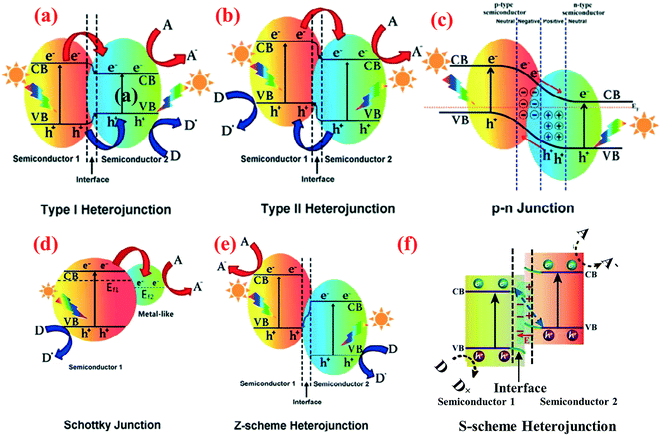 | ||
| Fig. 1 Band structure of various types of heterojunctions in a photocatalytic hybrid nanocomposite: (a) type I heterojunction, (b) type II heterojunction, (c) p–n junction, (d) Schottky junction, (e) Z-scheme heterojunction, and (f) S-scheme heterojunction. A, D and Ef represent electron acceptor, electron donor and Fermi level, respectively. Adapted with permission from ref. 55 and 138. Copyright 2019 Elsevier. | ||
| Heterojunction | Structure | Types | Light source | Application | Performance | Advantages | Disadvantages | |
|---|---|---|---|---|---|---|---|---|
| Yield (μmol h−1 g−1) | Efficiency (AQE) | |||||||
| g-C3N4/LaPO4 (ref. 67) | 1D/1D | Type II | Xe lamp (300 W) | CO2 reduction | CO 14.4 | — | Spatial separation of photo-generated electrons and holes | Weaker redox potential |
| CdS/g-C3N4 (ref. 69) | 1D/1D | Xe lamp (350 W) | H2 evolution Pt co-catalyst (0.6 wt%) | 4152 (λ ≥420 nm) | 4.3% (λ = 420 nm) | |||
| CdS/MoS2 (ref. 144) | 1D/2D | Xe lamp (300 W) | H2 evolution Pt co-catalyst (3 wt%) | 6020 (λ ≥400 nm) | 22.0% (λ = 475 nm) | |||
| CdS/ZnO (ref. 145) | 0D/1D | Xe lamp (500 W) | H2 evolution | 851 (λ ≥400 nm) | 3% (λ = 420 nm) | |||
| g-C3N4/TiO2 (ref. 79) | 0D/1D | Xe lamp (300 W) | H2 evolution | 4.58 (μmol h−1 cm−2) (λ ≥400 nm) | — | |||
| TiO2/MoS2 (ref. 146) | 1D/2D | Xe lamp (350 W) | CO2 reduction | CH4 2.86 CH3OH 2.55 | 0.16% (λ = 420 nm) | |||
| BiOBr/TiO2 (ref. 89) | 1D/2D | p–n | Xe lamp (300 W) | H2 evolution | 122 (>420 nm) | — | Internal electrostatic field induces rapid separation of photogenerated electrons and holes | Weaker redox potential |
| NiWO4/Zn0.7Cd0.3S (ref. 149) | 1D/2D | LED lamp (50 W) | H2 evolution | 15![[thin space (1/6-em)]](https://www.rsc.org/images/entities/char_2009.gif) 950 (>420 nm) 950 (>420 nm) |
— | |||
| WO3–CuO (ref. 147) | 1D/2D | Xe lamp (300 W) | CO2 reduction | CH4 0.84 | — | |||
| P3HT/ZnO (ref. 91) | 1D/1D | Xe lamp (300 W) | Degradation | — | — | |||
| P3HT/TiO2 (ref. 94) | 1D/1D | Xe lamp (70 W) | Photo-detectors | — | — | |||
| Fe–Ag/TiO2 (ref. 108) | 0D/1D | Schottky junction | Xe lamp (300 W) | Photocatalytic antibacterial | — | — | Cocatalysts, as charge carrier traps, can accelerate photo-generated carrier spatial separation and expand light absorption | Weaker redox potential |
| AuPd/ZnO (ref. 109) | 0D/1D | Xe lamp (300 W) | Water splitting activity | — | — | |||
| TiO2/GDY (ref. 118) | 1D/2D | Xe lamp (300 W) | CO2 reduction | CO 50.53 CH4 2.8 | 0.2% (λ = 400 nm) | |||
| CdS/Ti3C2 (ref. 148) | 1D/2D | Xe lamp (300 W) | H2 evolution | 2407 | 35.6% (λ = 420 nm) | |||
| WO3/Au/In2S3 (ref. 113) | 0D/1D | Z-scheme | Xe lamp (500 W) | CO2 reduction | CH4 0.42 (>420 nm) | — | Stronger redox potential; photo-generated carrier spatial separation | Difficult to characterize |
| g-C3N4/Pt/TiO2 (ref. 126) | 1D/2D | Xe lamp (500 W) | H2 evolution | 13.77 (>400 nm) | — | |||
| ZnIn2S4/TiO2 (ref. 130) | 1D/2D | Xe lamp (300 W) | CO2 reduction | CH4 1.135 (>420 nm) | — | |||
| CuInS2/TiO2 (ref. 131) | 1D/2D | Xe lamp (350 W) | CO2 reduction | CH4 2.5 CH3OH 0.86 | — | |||
| MoS2/Ag2Mo2O7 (ref. 133) | 1D/2D | Xe lamp (150 W) | Degradation | — | — | |||
| TiO2/CdS (ref. 140) | 1D/2D | S-scheme | Xe lamp (350 W) | H2 evolution | 2320 | — | Stronger redox potential; high Fermi level; photo-generated carrier spatial separation | Difficult to characterize |
| g-C3N4/Ag/Ag3VO4 (ref. 142) | 1D/2D | LED lamp (50 W) | Degradation | — | — | |||
2.1 Type II heterojunction
The type II photocatalytic system is the most common.56–58 In type II heterojunctions, photogenerated electrons in the CB of semiconductor 1 will transfer to the CB of semiconductor 2 under light irradiation, and the photogenerated holes in the VB of semiconductor 2 will be transferred to the VB of semiconductor 1 (Fig. 1b).54,59 Due to the internal electric field (IEF) formed at the interface between these two semiconductors, the photogenerated electron–hole pairs can be separated effectively, resulting in improved photocatalytic activity.60,61Taking advantage of the large specific area and unique structures of 1D nanomaterials, type II heterojunctions using 1D nanomaterials as substrates have been widely fabricated to broaden the light absorption of the photocatalyst and improve the separation efficiency of photogenerated electron–hole pairs.62–64 In particular, type II heterojunction photocatalysts with core–shell structures are most favorable because they effectively avoid agglomeration and provide a direct pathway for the rapid transport of photogenerated charge carriers.65,66 Furthermore, the large interfacial area between two semiconductors promotes rapid charge separation. For example, the g-C3N4/LaPO4 core/shell heterojunction photocatalyst has been demonstrated to be highly efficient for CO2 reduction.67 The CB and VB potentials of g-C3N4 are −0.88 and 1.98 eV, while the CB and VB potentials of LaPO4 are −0.74 and 3.11 eV, respectively (Fig. 2b). The more positive CB and VB levels of g-C3N4 than those of LaPO4 suggested that a type II heterojunction is easily constructed for photoinduced charge carrier transfer and separation. The g-C3N4/LaPO4 heterojunction photocatalyst exhibited excellent photocatalytic activity and stability ascribed to the well-matched band structure and extensive interface from close contact, which greatly enhances light sensitivity and effectively accelerates the charge carrier separation/transfer (Fig. 2a). Many other heterojunction photocatalysts with 1D core–shell structures such as TiO2/C3N4,68 C3N4/CdS,69 Ni3S2/VO2,70 and ZnO/WS2 (ref. 71) have also been reported to fit the type II photocatalytic system, which can greatly improve the separation and transfer efficiency of photogenerated pairs.
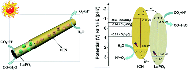 | ||
| Fig. 2 Schematic illustration of the proposed mechanism in the nanocomposite. Adapted with permission from ref. 67. Copyright 2017 Elsevier. | ||
Despite the many merits of type II core–shell structures, the light absorption of the 1D photocatalyst is weak because the core is almost completely covered by the shell layer. Therefore, type II heterojunctions with 3D (2D/1D) and 0D/1D structure are often utilized for photocatalysis.72,73 For example, a 3D heterojunction composite of ZnO nanosheets coated onto TiO2 nanowire arrays was designed as an efficient photoelectrode for photoelectrochemical (PEC) solar hydrogen production (Fig. 3).74 The unique 3D structure (2D/1D) of the ZnO/TiO2 heterojunction not only can greatly improve the light absorption due to the increased optical path by reducing reflection and multi-scattering but also can enable the electron–hole pairs to efficiently separate and enable charge carrier transport at the interface, resulting in significant enhancement of hydrogen generation in a neutral electrolyte solution. Meanwhile, the decoration of 1D nanomaterials with semiconductor quantum dots (0D/1D) is another method to fabricate type II heterojunctions. In particular, after decoration with small bandgap semiconductor quantum dots (QDs), the light absorption efficiency is enhanced. For example, TiO2 nanowires decorated by CdSe QDs have demonstrated an enhanced photoactivity in the wavelength region from 350 to 550 nm.75 ZnO nanowire arrays sensitized by CdTe QDs show significant photocurrent improvement.76 Similar type II 0D/1D structure heterojunctions such as CdS/ZnO,77 C3N4/ZnO,78 and C3N4/TiO2 (ref. 79) have been reported to improve the photocatalytic and PEC performance.
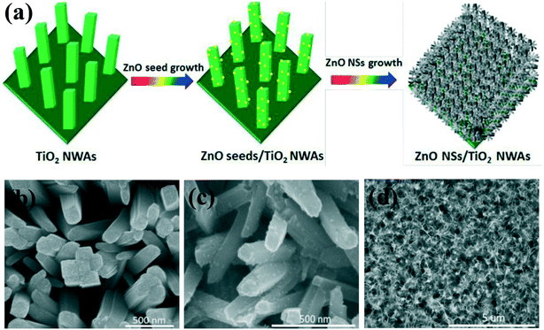 | ||
| Fig. 3 (a) Scheme for the fabrication of 3D ZnO/TiO2 2D/1D nanosheet–nanowire array architectures. (b–d) SEM images of (b) pure 1D TiO2 nanowire arrays, (c) ZnO seed nanoparticle-decorated 1D TiO2 nanowire arrays. (c) SEM images of 3D ZnO/TiO2 2D/1D nanosheet–nanowire array architectures fabricated in 0.1 M zinc nitrate aqueous solution. Adapted with permission from ref. 74. Copyright 2019 Royal Society of Chemistry. | ||
2.2 p–n type heterojunction
Although type II heterojunctions can in principle separate electron–hole pairs for 1D nanomaterial-based composites, they still cannot substantially address the issue of fast recombination of electron–hole pairs.54,82 To further suppress electron–hole pair recombination, the concept of p–n junction is proposed to accelerate electron–hole pair migration through the synergy between the band orientation of the interface and the internal electric field (IEF).79–87 In general, before light irradiation, electrons on the n-type semiconductor diffuse into the p-type semiconductor through the p–n junction interface. At the same time, holes in the p-type semiconductor tend to diffuse into the n-type semiconductor. The electron and hole diffusion will continue until the system reaches the Fermi level balance.86 As a result, an IEF is formed at the p–n junction interface (Fig. 1c). Under the synergy of the IEF and light irradiation, electrons and holes will migrate in a directional way, which greatly inhibits the recombination of electrons and holes and further improves the photocatalytic performance.Recently, a number of p–n heterojunction composite photocatalysts with hierarchical structures, such as core–shell, 3D (2D/1D), and 0D/1D structures, have been designed to improve the photocatalytic and photoelectrocatalytic activities.87,88 For instance, a 3D (2D/1D) structure of p–n junction composite photocatalyst has been constructed by assembling p-type BiOBr nanosheets on the surface of n-type TiO2 nanobelts. As shown in Fig. 4, the n-type TiO2 and p-type BiOBr have different Fermi levels. After contact, the Fermi level difference between them leads to electron transfer from TiO2 to BiOBr until the Femi levels of BiOBr and TiO2 reach an equilibrium state. Consequently, an IEF is formed between n-TiO2 and p-BiOBr. Driven by the IEF and light irradiation, the photogenerated carriers were effectively separated, resulting in enhanced photocatalytic activity.89 A (0D/1D) structure of p–n junction photocatalyst constructed by assembling p-type NiS nanoparticles on the surface of n-type CdS nanorods was reported to show enhanced H2-production activity (Fig. 5).90 In addition, organic/inorganic hybrid p–n heterojunctions based on a combination of p-type donor organic semiconductors with n-type acceptor inorganic semiconductors have been widely used in photocatalysis. For example, Lee et al. constructed a poly (3-hexylthiophene) (P3HT) nanomesh/ZnO nanorod p–n junction that showed the best visible light photodegradation rate of 80% within 30 minutes. The excellent photocatalytic activity of the composite is attributed to the enhanced visible-light absorption and separation efficiency of charge carriers, boosting numerous redox sites by the self-assembled p-type P3HT nanofibers on the surface of ZnO nanorods. At the same time, the fabrication of unique p–n nanorod heterojunctions effectively solves the weak chemical durability of organic semiconductors.91 In addition, similar enhanced photocatalytic and photoelectric performances have been observed in other organic/inorganic hybrid p–n heterojunctions such as polyaniline (PANI)/TiO2 nanofibers, polypyrrole (PPY)/TiO2 nanotubes, and P3HT/TiO2 nanofibers.92–94 Thus, the construction of organic/inorganic hybrid composites is regarded as a most effective and common method to form p–n heterojunctions, which is also widely applied in other research fields such as solar cells.
 | ||
| Fig. 4 (a) The band energy of BiOBr and TiO2 before contact and (b) the formation of the p–n junction and the charge transfer and separation process under visible light irradiation. Adapted with permission from ref. 79. Copyright 2016 Elsevier. | ||
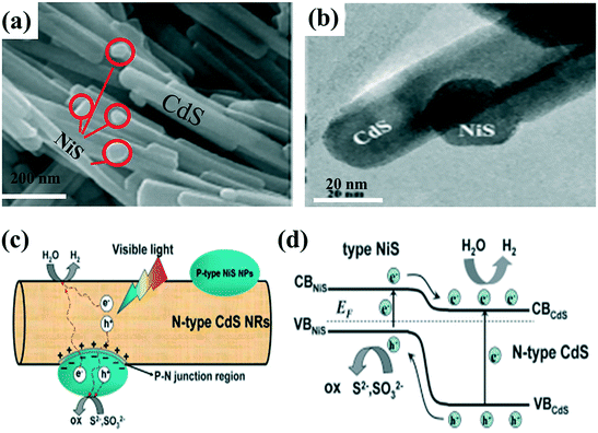 | ||
| Fig. 5 (a) SEM image of 5 wt% NiS-loaded CdS, (b) HRTEM image of as-prepared 5 wt% NiS-loaded CdS, (c) schematic diagram of charge transfer and separation, (d) the p–n junction band structure and schematic illustration of the electron–hole separation process under visible-light irradiation. Adapted with permission from ref. 90. Copyright 2013 Royal Society of Chemistry. | ||
2.3 Schottky junction
A Schottky junction is a heterojunction formed by combining semiconductor photocatalysts with appropriate cocatalysts such as Au, Ag, Pt, MoS2, and graphene. When n-type or p-type semiconductors with cocatalysts form Schottky junctions, the cocatalysts, as charge carrier traps, can promote the rapid transfer of photogenerated electrons in the CB or photogenerated holes in the VB to the cocatalyst, achieving spatial separation of photogenerated electrons and holes (Fig. 1d).91–100 In addition, due to the different Fermi levels of semiconductors, a Schottky barrier may be formed at the interface, which will effectively inhibit the backflow of electrons or holes from the cocatalyst to the semiconductor, forming a unidirectional flow channel from the photocatalyst to the cocatalyst (Fig. 6).95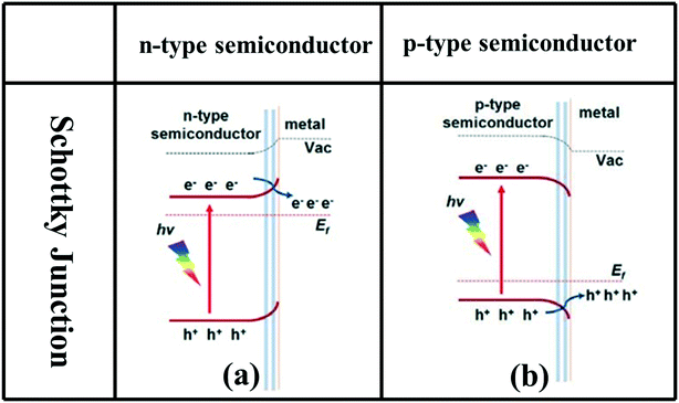 | ||
| Fig. 6 Schematic band diagrams illustrating the charge transfer driven by the Schottky junction between metal and n-type (a) or p-type (b) semiconductor. Adapted with permission from ref. 95. Copyright 2015 Wiley. | ||
Construction of a Schottky junction by choosing a suitable cocatalyst load onto the 1D nanomaterial is one of the effective methods to promote the separation of photogenerated carriers, accelerate the surface reaction rate, and improve the selectivity of products.95 Thus, many kinds of cocatalysts have been used to modify 1D nanomaterials to improve the photocatalytic and photoelectric activities. Besides promoting the separation of photogenerated carriers, cocatalysts can also form reactive sites to accelerate the surface reaction rate.101–103 Noble metals such as Au, Ag and Pt are the most common cocatalysts used. Metallic cocatalysts assembled on the surface of 1D nanomaterials can form Schottky junctions with photocatalysts, which can expand light absorption in addition to enhancing charge separation, resulting in the enhancement of the catalytic activity.104 In addition, except for monometallic cocatalysts, bimetallic cocatalysts may have greater potential in catalytic applications because the activity, selectivity and light absorption of the photocatalyst can be drastically influenced by the presence of a second metal.105,106 1D photocatalysts such as TiO2, ZnO and Cd0.5Zn0.5S decorated by bimetallic cocatalysts including AuPd, FeAg or PtCo have shown higher H2 production activity than their corresponding monometallic counterparts.107–110 Yu et al.111 designed a well-defined Au@Pt core–shell nanostructure as a cocatalyst to construct a TiO2 nanotube-Au (core)–Pt (shell) system for photocatalytic hydrogen generation (Fig. 7). Au can induce localized surface plasmon resonance (SPR) under light irradiation and provide a beneficial electric field nearby to facilitate the separation of photoexcited carriers, while the Pt shell with porous architecture and a high surface area can offer more active sites for the hydrogen evolution rate (HER). This Au@Pt core–shell cocatalyst system combines the characteristics of the localized surface plasmon effect of gold and the excellent ability of proton reduction of platinum, which has a synergistic effect for photocatalytic hydrogen generation.111–113
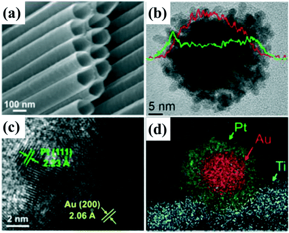 | ||
| Fig. 7 (a) SEM images of TiO2 nanotubes. (b) Elemental line-scan of Au@Pt nanostructure. (c) High-resolution TEM image and corresponding lattice fringe of Au (200) and Pt (111) planes. (d) Corresponding high-angle annular dark field (HAADF) micrograph and elemental mapping of Ti, Au, and Pt. adapted with permission from ref. 111. Copyright 2016 Royal Society of Chemistry. | ||
Recently, the rational design of spatially separated dual cocatalysts on photocatalysts has attracted extensive attention since charge separation can be further promoted by loading reductive and oxidation cocatalysts simultaneously. Due to the larger surface area and long light irradiation pathway of 1D nanomaterials, the use of 1D photoelectrodes and photocatalysts decorated with spatially separated dual cocatalysts is recognized as an effective and promising method for improving the photocatalytic and photoelectric activities.115 Qin et al.114 prepared a Pt/TiO2 nanotube/CoOx composite photocatalyst with Pt nanoparticles on the inner surface of TiO2 nanotubes and CoOx nanoclusters on the outer surface (Fig. 8). The spatially separated Pt and CoOx dual cocatalysts, acting as electron and hole collectors, respectively, have a synergetic effect on the separation of photogenerated carriers, achieving remarkably high photocatalytic efficiency. Similarly, the construction of photoelectrodes with spatially charge separated oxidation and reduction cocatalysts have been demonstrated to improve the photoelectrode for photoelectrochemical (PEC) conversion efficiency. For example, Wang116et al.116 employed a simple but effective “bottom-up” method, metallic replacement combined with hydrolytic reactions, to selectively grow FeOOH and Pt cocatalysts on hematite nanoflake photoanodes (FeOOH/α-Fe2O3 nanofiber/Pt). Pt nanoparticles function as an electron acceptor and transfer layer to facilitate water reduction, and FeOOH is regarded as an active site to promote interfacial hole transfer, This novel FeOOH/α-Fe2O3 nanofiber/Pt photoanode shows excellent performance for the PEC water splitting reaction. Likewise, in order to further improve the light absorption and reduce the charge recombination rate, Liu117et al.117 studied a quaternary system including ZnO nanorods, CdS nanoparticles, Au and FeOOH simultaneously. ZnO nanorods are firstly modified by CdS nanoparticles to broaden the light absorbance spectrum and reduce charge recombination. Then Au and FeOOH cocatalysts decorated on inner and outer surface sites of the photocatalysts can drive photogenerated electrons and holes to flow in opposite directions, further promoting charge separation and PEC performance.
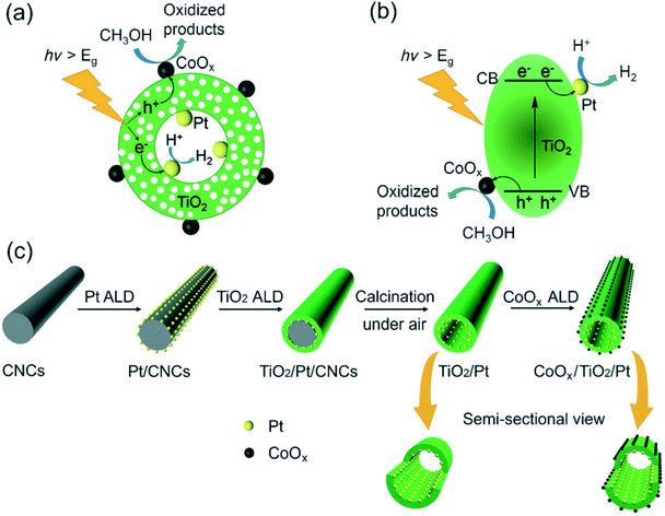 | ||
| Fig. 8 The proposed mechanism for photocatalytic hydrogen production mediated by CoOx/TiO2/Pt. (a) The reaction process. (b) Band structure of the photocatalysts. (c) Synthetic process for TiO2/Pt and CoOx/TiO2/Pt photocatalysts by template-assisted ALD. Adapted with permission from ref. 114. Copyright 2017 Wiley. | ||
Considering the high price of noble metals, new and efficient cocatalysts such as organic cocatalysts have been explored to boost the photocatalytic reduction activity. Xu et al.118 synthesized a new Schottky junction using graphdiyne (GDY) cocatalyst coupled TiO2 nanofibers for enhancing photocatalytic CO2 reduction efficiency (Fig. 9a and b). First-principle calculations and in situ X-ray photoelectron spectroscopy (XPS) measurements show that there may be electron transfer or a strong chemical interaction between TiO2 and GDY, resulting in the formation of an IEF at the interfaces between GDY and TiO2 (Fig. 9c). In addition, GDY has strong chemisorption to CO2 molecules that can enhance CO2 adsorption and activation as well as accelerate catalytic reactions over the TiO2/GDY heterostructure. The formed IEF, in conjunction with the photothermal effect and strong chemisorption of GDY on CO2 molecules, leads to significantly improved CO2 photoreduction efficiency.
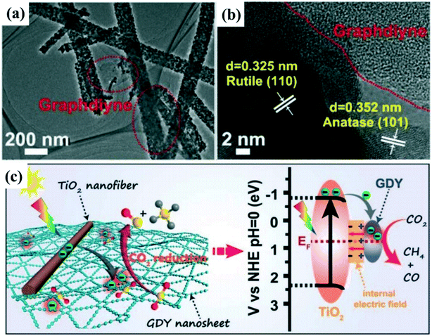 | ||
| Fig. 9 (a and b) TEM and HRTEM images of 0.5 wt% graphdiyne (GDY) loaded TiO2 nanofibers. (c) Schematic illustration of TiO2/GDY heterojunction: internal electric field-induced charge transfer and separation under UV-visible light irradiation for CO2 photoreduction. Adapted with permission from ref. 118. Copyright 2019 Wiley. | ||
2.4 Z-scheme heterojunction
One issue with type II heterojunction, p–n heterojunction and Schottky junction is that the redox ability of photoexcited electrons and holes for each reaction is often weakened by the fact that the photogenerated electrons in the CB of semiconductor 1 could transfer to the CB of semiconductor 2 with relatively more positive band energy (Fig. 1e), and the photogenerated holes could transfer to the VB of the semiconductor with a more negative band energy due to the well-matched bandgap energy levels between these two semiconductors.119,120 Inspired by the mechanism of natural photosynthesis (NPS) in green plants, the construction of an artificial Z-scheme system by two connected semiconductor photocatalysts might overcome this problem.121 Specifically, in a typical Z-scheme photocatalytic system, the photogenerated electrons in semiconductor 1 would transfer and recombine with the photogenerated holes in semiconductor 2, giving the photogenerated electrons a relatively higher position and the photogenerated holes a lower position to participate in the redox reactions.122Recently, the design and synthesis of Z-scheme 1D nanomaterial-based heterojunctions with hierarchical structures have been studied for photocatalytic hydrogen production, photocatalytic CO2 reduction and PEC reactions.54,121 Initially, Z-scheme photocatalytic systems consisting of two semiconductors and a solid-state electron mediator at the interface of two photocatalysts were developed for water splitting.119,122 Noble metal particles (such as Au, Ag) and reduced graphene oxide (RGO) were explored as electron mediators to accelerate the transport of photogenerated electrons and holes.120 For example, Z-scheme WO3/Au/In2S3 nanowire arrays123 were successfully constructed through a two-step vapor deposition process (Fig. 10a and b). A photo-assisted Kelvin probe force microscope (KPFM) technique was utilized to detect the interfacial charge transfer of Z-scheme WO3/Au/In2S3 nanowires, showing that the vectorial hole transfer of In2S3 → Au → WO3 occurs upon excitation of both WO3 and In2S3. Au nanoparticles embedded between WO3 and In2S3, working as charge mediators, can accelerate the recombination between the photogenerated electrons in the CB of WO3 and the photogenerated holes in the VB of In2S3, leaving the photogenerated electrons in the CB of In2S3 and the photogenerated holes in the VB of WO3 with a strong redox ability (Fig. 10c). Therefore, a strong charge carrier separation ability and redox ability of the unique Z-scheme photocatalytic system provide the WO3/Au/In2S3 heterostructure with great photocatalytic activity toward CO2 reduction (Fig. 10d). Similarly, other Z-scheme system-based 1D photocatalysts with noble-metal nanoparticles as electron mediators, such as TiO2/Au/Cu2O, CdS/Ag/TiO2, g-C3N4/Pt/TiO2, have also been reported to exhibit enhanced photocatalytic activities.124–126
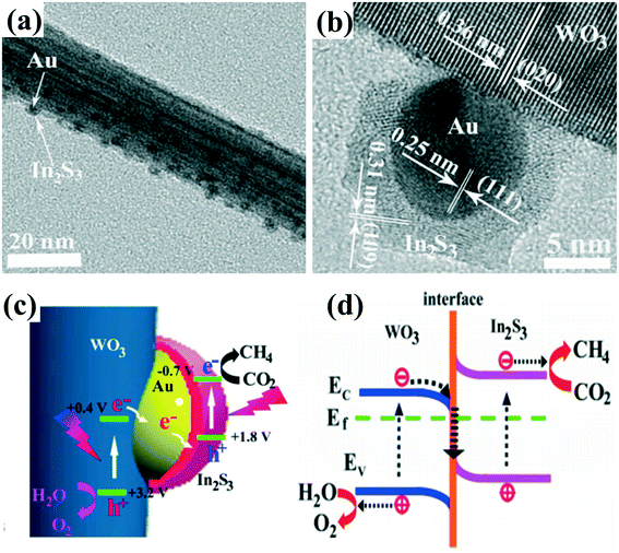 | ||
| Fig. 10 (a and b) TEM and HRTEM images of WO3/Au/In2S3. (c) Schematic illustration of the charge separation and transfer in the Z-scheme system of WO3/Au/In2S3. (d) The interfacial electron transfer between WO3 and In2S3. Adapted with permission from ref. 123. Copyright 2016 American Chemical Society. | ||
In addition to noble metals, some low-cost nonmetal materials such as reduced graphene oxide (RGO) with excellent conductivity can also be explored as electron mediators in indirect Z-scheme systems.120 For example, a Z-scheme (TNT–GR–CdS) system with graphene (GR) film as the electron mediator in contact with both TiO2 nanotube (TNT) arrays and CdS QDs was constructed to be applied in waste water treatment.127 Under ultraviolet visible (UV-vis) light irradiation, the photoexcited electrons in the CB of the TiO2 nanotube are transferred to GR and then to the VB of CdS, subsequently recombining with the holes photogenerated in CdS. The remaining VB holes of the TNT with a strong oxidation power oxidize dyes or H2O to produce hydroxyl radicals (˙OH). The charge transport of this Z-scheme system not only achieves efficient spatial separation of photogenerated carriers and keeps the photogenerated electron and hole with strong reduction and oxidation ability but also restricts the photocorrosion of CdS, leading to the high photocatalytic activity and photostability of the TNT–GR–CdS composite film (Fig. 11). Similarly, Zhou et al.128 fabricated a Fe2V4O13 nanoribbon/reduced graphene oxide (RGO)/CdS nanoparticle (Z-scheme system) composite photocatalyst for photoconversion of gaseous CO2 to methane. The Z-scheme photocatalytic system leads to more efficient spatial separation of the electrons and holes and subsequent high photoconversion efficiency of CO2.
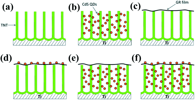 | ||
| Fig. 11 Design and architectures of (a) the original TiO2 nanotube (TNT) electrode, (b) the TNT–CdS quantum dots (QDs), (c) the TNT–graphene (GR), (d) the TNT–GR–CdS, (e) the TNT–CdS–GR, and (f) the TNT–CdS–GR–CdS composite film electrodes. Adapted with permission from ref. 127. Copyright 2014 American Chemical Society. | ||
Although Z-scheme systems with appropriate mediators have been well developed and applied to water splitting, CO2 reduction and pollutant degradation, the preparation of ternary system composite photocatalysts consisting of two semiconductors and an electron mediator is often complex. In addition, due to the surface plasmon resonance (SPR) effect of noble metals, the electron mediator can absorb visible light, consequently affecting the photocatalytic activity. Therefore, the fabrication of direct Z-scheme system photocatalysts without redox mediators has aroused widespread interest in recent years. Like the type II heterojunction, direct Z-scheme 1D-based composite photocatalysts with core–shell, 3D (2D/1D) and 0D/1D structures have been designed and investigated to improve the photocatalytic activity.120,129 In our previous work,130 a Z-scheme 3D ZnIn2S4/TiO2 composite photocatalyst was constructed by assembling 2D ZnIn2S4 nanosheets onto 1D TiO2 nanobelts for photocatalytic CO2 reduction (Fig. 12a and b). The unique 3D morphology not only provides a large surface area but also promotes the separation and transfer of photogenerated electrons and holes. This 3D ZnIn2S4/TiO2 composite photocatalyst demonstrated excellent photocatalytic reduction activity, about 39 times higher than that of bare ZnIn2S4 nanosheets. The enhanced photocatalytic activity is ascribed to the unique 3D structure and effective separation of the charge carriers between ZnIn2S4 and TiO2 in the Z-scheme system (Fig. 12c). In order to determine whether a ZnIn2S4/TiO2 composite photocatalyst is a direct Z-scheme photocatalytic system rather than a type II heterojunction system, photoluminescence (PL) spectra and transient time-resolved PL decay measurements were employed. In addition, the band potentials of ZnIn2S4 and TiO2 corresponding with reaction products can further confirm this proposal. Similarly, other Z-scheme 3D structure (2D/1D) composite photocatalysts, such as TiO2/CuInS2, 1D/2D carbon nanotubes (CNTs)/protonated carbon nitrides (p-C3N4), and MoS2/Ag2Mo2O7 have also been reported to exhibit enhanced photocatalytic activities.131–133 Except for some Z-scheme 3D structure (2D/1D) heterojunctions, a number of composite photocatalysts with 0D/1D structure have been constructed as Z-scheme systems. For example, graphene quantum dot (GQD) decorated ZnO nanowires (0D GQD/1D ZnO)134 are proposed to follow a direct Z-scheme system heterojunction, which showed a considerable improvement in the photocatalytic degradation of methylene blue with about 3-fold enhancement as compared to pure ZnO nanowires. Similar enhancement of photocatalytic and photoelectric activity has been observed in other 0D/1D direct Z-scheme heterojunctions such as CdS QDs/CeO2 nanorods,135 Co2P nanoparticles/CdS nanorods,136 and InVO4 nanoparticles/β-AgVO3 nanoribbons.137 Based on the mechanisms of photogenerated charge transfer, Z-scheme systems have more advantages for photocatalysis than type II systems. Thus, a variety of heterojunctions has been constructed according to the Z-scheme concept. Many characteristic methods such as time-resolved photoluminescence (PL), Kelvin probe force microscopy (KPFM), photochemical tests, and trapping experiments have been used to demonstrate the transfer pathways of electrons and holes. However, there is no direct evidence for the actual transfer paths for photogenerated carriers. Thus, it is still a challenge to find a new characteristic method to directly confirm the Z-scheme system.
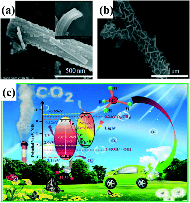 | ||
| Fig. 12 (a and b) SEM images of TiO2 nanobelts and ZnIn2S4/TiO2. (c) Schematic diagrams for energy bands of TiO2 nanobelts and ZnIn2S4 nanosheets and the transfer of photogenerated electrons from TiO2 to ZnIn2S4 forming a Z-scheme system under UV-vis light irradiation. Adapted with permission from ref. 130. Copyright 2017 Elsevier. | ||
2.5 S-scheme heterojunction
Recently, Yu et al. proposed a new step scheme (S-scheme) system heterojunction. Like the Z-scheme system, it can provide a stronger redox ability and promote separation and transfer of photoexcited carries.138 Specifically, S-scheme heterojunctions consist of two n-type semiconductors 1 and 2 (Fig. 1f). Semiconductor 1 is an oxidized photocatalyst with a larger work function and a lower Fermi energy level, and semiconductor 2 is a reductive photocatalyst with a smaller work function and a higher Fermi energy level. The transfer pathway of photo-excited charge in the S-scheme heterojunctions is more like a “step” or “N”, which means the electrons from the CB of semiconductor 1 recombine with the holes in the VB of semiconductor 2, then the electrons and holes with stronger reduction and oxidation ability are separated spatially. Furthermore, due to the difference in the Fermi energy levels between the two semiconductors, the electrons of semiconductor 1 will continue to transfer to semiconductor 2 until the Fermi energy levels are at equilibrium when the heterojunction is formed. As a result, an IEF is formed at the interface between these two semiconductors, which is the main driving force for the photogenerated carrier migration.1391D nanomaterial-based S-scheme system heterojunctions have been designed and fabricated to accelerate the separation and transfer efficiency of photogenerated charges. For example, a TiO2/CdS core–shell S-scheme heterojunction prepared by an in situ electrospinning method showed excellent H2 generation activity, which is 35 times higher than that of pure 1D TiO2 nanofibers (Fig. 13).140 The enhanced photocatalytic activity can be attributed to the synergy between the core–shell structure and the rapid transfer of photogenerated carriers in the S-scheme photosystem. The S-scheme heterojunction was confirmed by XPS analysis and density functional theory (DFT) calculations. Another S-scheme heterojunction based on Bi2O3 nanoparticle modified TiO2 nanotube (Bi2O3/TiO2) was found to improve the photocatalytic degradation performance for phenol.141 In addition to binary composite photocatalysts, some 1D nanomaterial-based ternary heterojunctions with an S-scheme photosystem have also been reported to improve photocatalytic activity. For instance, Mei et al. constructed a porous g-C3N4/Ag/Ag3VO4 S-scheme by a chemical deposition method that showed the best photodegradation rate of 99.3% within 8 min.142 The Ag particles not only have a role of charge mediator to promote the recombination of the photogenerated electrons in the CB of Ag3VO4 with the photogenerated holes in the VB of Pg-C3N4 but also have an SPR effect to enhance visible light absorption (Fig. 14). A similar ternary S-scheme g-C3N4/Bi/BiVO4 heterojunction was applied to improve CO2 reduction.143 In this work, the metal Bi has the same role as that of Ag particles in the above work. In fact, the S-scheme system heterojunction is a kind of Z-scheme system heterojunction. They have the same transfer mechanism of photogenerated carriers. The difference between these two semiconductors is that the S-scheme system heterojunction is composed of two n-type semiconductors with suitable Fermi energy levels. Thus, most research studies seldom distinguish S-scheme system heterojunctions from Z-system heterojunctions. Both systems can facilitate the separation efficiency of photogenerated carriers and improve the photocatalytic activity.
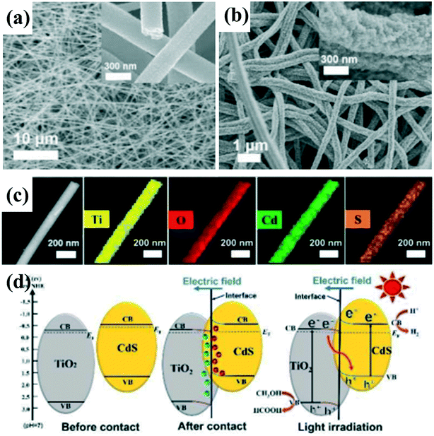 | ||
| Fig. 13 FESEM images of (a) T, and (b) TC10. (c) STEM image of 10 wt% CdS-loaded TiO2 nanofibers and the corresponding EDX elemental mappings of Ti, O, Cd, and S. (d) Schematic of the S-scheme pathway for charge carrier separation in TiO2/CdS nanofibers. Adapted with permission from ref. 140. Copyright 2019 Wiley. | ||
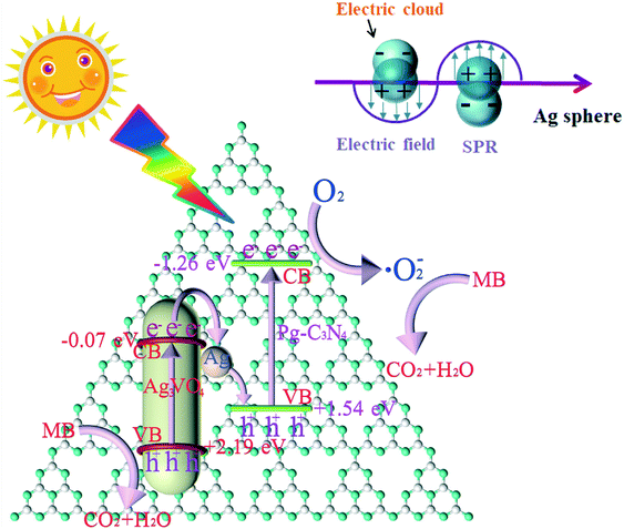 | ||
| Fig. 14 The possible charge transfer diagram of Pg-C3N4/Ag3VO4 composites. Adapted with permission from ref. 142. Copyright 2019 Elsevier. | ||
3 Summary and perspective
In summary, 1D nanomaterials have attracted considerable interest in photocatalysis and photoelectrocatalysis owing to their many advantages including large surface area, rapid and long-distance electron transport, and improved light absorption and scattering. In particular, due to their morphology, 1D nanomaterials have been widely used as excellent building blocks to construct heterojunctions for solving the bottleneck problem of fast recombination of photogenerated carriers. 1D-based heterostructured photocatalysts with various types of hierarchical structures have been designed and demonstrated to enhance the separation and transfer efficiency of photogenerated charge carriers, consequently improving the photocatalytic and photoelectrocatalytic activities. Due to the different preparation methods, band energies, morphologies, and structures, heterostructured photocatalysts exhibit different photogenerated charge transfer mechanisms and photocatalytic activities. We have discussed several mechanisms of photogenerated charge carriers in 1D nanomaterial-based heterojunctions, including type II heterojunction, p–n type heterojunction, Schottky junction, Z-type heterojunction and S-type heterojunction.Despite great progress made to date, there are still many challenges remaining for photocatalytic and photoelectrocatalytic applications of 1D nanomaterials and improvements are needed. First, the apparent quantum efficiency and separation efficiency of photogenerated charges in photocatalysis are generally still low. To develop new 1D-based composite photocatalysts with different hierarchical structures and optimal control of composition at the atomic level is highly desired. For example, use of advanced technology and equipment such as atomic-layer deposition (ALD) method and microsynthesis should be exploited to achieve more accurate design and control. Second, most current characterization methods, such as electron paramagnetic resonance (EPR), reactive species scavenging, XPS characterization, and terephthalic acid-assisted PL spectroscopy, cannot provide direct evidence about the pathway of electron and hole transfer. It is of strong interest to develop more advanced characterization methods to directly probe the charge transfer pathways and gain deeper mechanistic insight. With rational structural design/control and more in-depth mechanistic probes, it is expected that 1D nanomaterials will play a major role in photocatalysis and photoelectrocatalysis in the future.
Conflicts of interest
The authors declare no conflict of interest.Acknowledgements
This work was partly supported by the National Natural Science Foundation of China (No. 21978276), the Fundamental Research Funds for the Central Universities (Grant No. 2652019157; 2652019158; 2652019159), and the Innovation Ability Improvement Project of Hebei Province, China (No. 20543601D).References
- J. Deng, Y. Su and D. Liu, Chem. Rev., 2019, 119, 9221–9259 CrossRef CAS PubMed.
- L. Hao, L. Kang and H. Huang, Adv. Mater., 2019, 31, 1900546 CrossRef PubMed.
- J. Barber, Chem. Soc. Rev., 2009, 38, 185–196 RSC.
- T. A. Faunce and W. Lubitz, Energy Environ. Sci., 2013, 6, 695–698 RSC.
- J. M. Foley, M. J. Price and J. I. Feldblyum, Energy Environ. Sci., 2012, 5, 5203–5220 RSC.
- Z. R. Tang, F. Li, Y. Zhang, X. Fu and Y. J. Xu, J. Phys. Chem. C, 2011, 115, 7880 CrossRef CAS.
- A. I. Hochbaum, R. Chen, R. D. Delgad, W. Liang, E. C. Garnett, M. Najarian, A. Majumdar and P. Yang, Nature, 2008, 451, 163 CrossRef CAS PubMed.
- O. Khaselev and J. A. Turner, Science, 1998, 280, 425 CrossRef CAS PubMed.
- J. Li and G. F. Zheng, Adv. Sci., 2017, 4, 1600380–1600394 CrossRef PubMed.
- M. Tahir, J. CO2 Util., 2020, 37, 134–146 CrossRef CAS.
- M. Tahir and B. Tahir, Appl. Surf. Sci., 2019, 485, 450–461 CrossRef CAS.
- B. Tahir and M. Tahir, Appl. Surf. Sci., 2019, 506, 145034 CrossRef.
- J. Di, J. Xia and M. F. Chisholm, Adv. Mater., 2019, 31, 1807576–1807576 CrossRef PubMed.
- I. S. Cho, Z. Chen and A. J. Forman, Nano Lett., 2011, 11, 4978–4984 CrossRef CAS PubMed.
- S. J. Peng, L. L. Li, J. K. Y. Lee, L. L. Tian, M. Srinivasan, S. Adams and S. Ramakrishna, Nano Energy, 2016, 22, 361–395 CrossRef CAS.
- K. Yu, X. Pan and G. Zhang, Adv. Energy Mater., 2018, 8, 1802369 CrossRef.
- C. K. Chan, H. Peng, G. Liu, K. Mcilwrath, X. F. Zhang, R. A. Huggins and Y. Cui, Nat. Nanotechnol., 2008, 3, 31 CrossRef CAS.
- B. Liu, A. Khare and E. S. Aydil, ACS Appl. Mater. Interfaces, 2011, 3, 4444 CrossRef CAS.
- M. Tahir and B. Tahir, Chem. Eng. J., 2020, 400, 125868 CrossRef CAS.
- J. L. Liu, C. X. Guo, A. Vasileff and S. Z. Qiao, Small Methods, 2017, 1, 1600006–1600012 CrossRef.
- J. Di, J. X. Xia, M. X. Ji, L. Xu, S. Yin, Z. G. Chen and H. M. Li, J. Mater. Chem. A, 2016, 4, 5051–5061 RSC.
- F. Song and X. L. Hu, Nat. Commun., 2014, 5, 4477 CrossRef CAS PubMed.
- D. H. Deng, K. S. Novoselov, Q. Fu, N. F. Zheng, Z. Q. Tian and X. H. Bao, Nat. Nanotechnol., 2016, 11, 218–230 CrossRef CAS PubMed.
- R. C. Alkire, P. N. Bartlett, J. Lipkowski and Z. Phys, Chem, 2015, 195, 284–285 Search PubMed.
- A. K. Azmat and T. Muhammad, J. CO2 Util., 2019, 29, 205–239 CrossRef.
- S. Tasleem and M. Tahir, Int. J. Hydrogen Energy, 2020, 45, 19078–19111 CrossRef CAS.
- M. Tahir, S. Tasleem and B. Tahir, Int. J. Hydrogen Energy, 2020, 45, 15986–16038 Search PubMed.
- Y. Xia, P. Yang, Y. Sun, Y. Wu, B. Mayers, B. Gates, Y. Yin, F. Kim and H. Yan, Adv. Mater., 2003, 15, 353 CrossRef CAS.
- D. Moitra, C. Anand, B. K. Ghosh, M. Chandel and N. N. Ghosh, ACS Appl. Energy Mater., 2018, 1, 464 CrossRef CAS.
- J. Tian, Z. Zhao and A. Kumar, Chem. Soc. Rev., 2014, 43, 6920 RSC.
- S. G. Kumar and L. G. Devi, J. Phys. Chem. A, 2011, 115, 13211–13241 CrossRef CAS.
- A. Fujishima and K. Honda, Nature, 1972, 238, 37 CrossRef CAS PubMed.
- J. H. Ha, P. Muralidharan and D. K. Kim, J. Alloys Compd., 2009, 475, 446–451 CrossRef CAS.
- Y. Zhong, Z. He and D. Chen, Appl. Surf. Sci., 2019, 467, 740–748 CrossRef.
- J. Di, C. Zhu and M. Ji, Angew. Chem., 2018, 130, 15063–15067 CrossRef.
- N. Wetchakun, S. Chaiwichain, B. Inceesungvorn, K. Pingmuang, S. Phanichphant, A. I. Minett and J. Chen, ACS Appl. Mater. Interfaces, 2012, 4, 3718 CrossRef CAS PubMed.
- Z. L. Wang, Adv. Mater., 2000, 12, 1295 CrossRef CAS.
- M. L. Terranova, Chem. Vap. Deposition, 2006, 12, 313–313 CrossRef CAS.
- Y. G. Sun, B. T. Mayers and Y. N. Xia, Nano Lett., 2002, 2, 481 CrossRef CAS.
- Y. J. Zhang, N. L. Wang, S. P. Gao, R. R. He, S. Miao, J. Liu, J. Zhu and X. Zhang, Chem. Mater., 2002, 14, 3564 CrossRef CAS.
- P. N. Dunn, Solid State Technol., 1994, 37, 49 Search PubMed.
- L. Mai, Y. Fan, Y. Zhao, X. Xu, L. Xu and Y. Luo, Nat. Commun., 2011, 2, 381 CrossRef PubMed.
- X. Xia, D. Chao, Z. Fan, C. Guan, X. Cao, H. Zhang and H. J. Fan, Nano Lett., 2014, 14, 1651 CrossRef CAS.
- J. Yin, Y. Li, F. Lv, Q. Fan, Y. Q. Zhao, Q. Zhang, W. Wang, F. Cheng, P. Xi and S. Guo, ACS Nano, 2017, 11, 2275 CrossRef CAS PubMed.
- W. Xiong, X. Pan, Y. Li, X. Chen, Y. Zhu, M. Yang and Y. Zhang, Mater. Lett., 2015, 157, 23 CrossRef CAS.
- L. Li, H. Yang, J. Yang, L. Zhang, J. Miao, Y. Zhang, C. Sun, W. Huang, X. Dong and B. Liu, J. Mater. Chem. A, 2016, 4, 1319 RSC.
- N. Choudhary, C. Li, H. S. Chung, J. Moore, J. Thomas and Y. Jung, ACS Nano, 2016, 10, 10726 CrossRef CAS.
- R. Liu, J. Duay and S. B. Lee, Chem. Commun., 2011, 47, 1384 RSC.
- Y. Dong, S. Li, K. Zhao, C. Han, W. Chen, B. Wang, L. Wang, B. Xu, Q. Wei, L. Zhang, X. Xu and L. Mai, Energy Environ. Sci., 2015, 8, 1267 RSC.
- L. Mai, Q. Wei, Q. An, X. Tian, Y. Zhao, X. Xu, L. Xu, L. Chang and Q. Zhang, Adv. Mater., 2013, 25, 2969 CrossRef CAS PubMed.
- P. Yang and J. M. Tarascon, Nat. Mater., 2012, 11, 560 CrossRef CAS PubMed.
- H. Wang, L. Zhang and Z. Chen, Chem. Soc. Rev., 2014, 43, 5234–5244 RSC.
- P. Murugesan, J. A. Moses and C. Anandharamakrishnan, J. Mater. Sci., 2019, 1–30 Search PubMed.
- J. Low, C. Jiang and B. Cheng, Small Methods, 2017, 1, 1700080 CrossRef.
- Y. Ren, D. Zeng and W. J. Ong, Chin. J. Catal., 2019, 40, 289–319 CrossRef CAS.
- R. Marschall, Adv. Funct. Mater., 2014, 24, 2421 CrossRef CAS.
- W. Chen, Y. X. Hua, Y. Wang, T. Huang, T. Y. Liu and X. H. Liu, J. Catal., 2017, 349, 8–18 CrossRef CAS.
- H. Wang, X. Yuan, H. Wang, X. Chen, Z. Wu, L. Jiang, W. Xiong and G. Zeng, Appl. Catal., B, 2016, 193, 36–46 CrossRef CAS.
- S. Wang and B. Y. Guan, J. Am. Chem. Soc., 2018, 140, 5037–5040 CrossRef CAS.
- X. Xiao, R. Hao and M. Liang, J. Hazard. Mater., 2012, 233-234, 122–130 CrossRef CAS.
- D. Jiang, J. Li, C. Xing, Z. Zhang, S. Meng and M. Chen, ACS Appl. Mater. Interfaces, 2015, 7, 19234–19242 CrossRef CAS PubMed.
- R. Ghosh Chaudhuri and S. H. Paria, Chem. Rev., 2012, 112, 2373–2433 CrossRef CAS.
- T. Jin, Q. Q. Han, Y. J. Wang and L. F. Jiao, Small, 2018, 14, 1703086–1703111 CrossRef PubMed.
- Q. L. Wei, F. Y. Xiong, S. S. Tan, L. Huang, E. H. Lan, B. Dunn and L. Q. Mai, Adv. Mater., 2017, 29, 1602300–1602338 CrossRef PubMed.
- J. Liu, J. Jiang and C. Cheng, Adv. Mater., 2011, 23, 2076–2081 CrossRef CAS PubMed.
- S. Kim, B. Fisher and J. Eisler, J. Am. Chem. Soc., 2003, 125, 11466–11467 CrossRef CAS PubMed.
- M. Li, L. Zhang and X. Fan, Appl. Catal., A, 2017, 201, 629–635 CrossRef CAS.
- Y. Wang, Q. Wu and Y. Li, J. Mater. Sci., 2018, 53, 11015–11026 CrossRef CAS.
- J. Zhang, Y. Wang and J. Jin, ACS Appl. Mater. Interfaces, 2013, 5, 10317–10324 CrossRef CAS PubMed.
- Q. Lv, L. Yang and W. Wang, J. Mater. Chem., 2019, 7, 1196–1205 RSC.
- E. Butanovs, S. Vlassov and A. Kuzmin, ACS Appl. Mater. Interfaces, 2018, 10, 13869–13876 CrossRef CAS.
- R. M. Alenezi, S. J. Henley and N. G. Emerson, Nanoscale, 2014, 6, 235–247 RSC.
- A. Kargar, K. Sun and Y. Jing, ACS Nano, 2013, 7, 9407–9415 CrossRef CAS.
- H. Han, W. Wang and L. Yao, Catal. Sci. Technol., 2019, 9, 1989–1997 RSC.
- H. Wang, G. Wang, Y. Ling, M. Lepert, C. Wang, J. Z. Zhang and Y. Li, Nanoscale, 2012, 4, 1463–1466 RSC.
- H. He, L. Gan and L. Sun, Appl. Phys. A: Mater. Sci. Process., 2017, 123, 613 CrossRef.
- G. Wang, X. Yang and F. Qian, Nano Lett., 2010, 10, 1088–1092 CrossRef CAS PubMed.
- X. Shen, L. Duan and J. Li, Mater. Res. Express, 2018, 6, 4 Search PubMed.
- G. Li, Z. Lian and W. Wang, Nano Energy, 2016, 446–454 CrossRef CAS.
- L. Li, P. A. Salvador and G. S. Rohrer, Nanoscale, 2014, 6, 24 RSC.
- J. Cao, X. Li, H. Lin, S. Chen and X. Fu, J. Hazard. Mater., 2012, 239, 316 CrossRef.
- Y. Peng, M. Yan, Q. G. Chen, C. M. Fan, H. Y. Zhou and A. W. Xu, J. Mater. Chem. A, 2014, 2, 8517 RSC.
- G. Liu, G. Zhao, W. Zhou, Y. Liu, H. Pang, H. Zhang, D. Hao, X. Meng, P. Li, T. Kako and J. Ye, Adv. Funct. Mater., 2016, 26, 6822–6829 CrossRef CAS.
- D. Jiang, L. Chen, J. Zhu, M. Chen, W. Shi and J. Xie, Dalton Trans., 2013, 42, 15726–15734 RSC.
- J. Lin, J. Shen, R. Wang, J. Cui, W. Zhou, P. Hu, D. Liu, H. Liu, J. Wang, R. I. Boughton and Y. Yue, J. Mater. Chem., 2011, 21, 5106 RSC.
- Z. Cai, Y. Zhou, S. Ma, S. Li, H. Yang, S. Zhao, X. Zhong and W. Wu, J. Photochem. Photobiol., A, 2017, 348, 168–178 CrossRef CAS.
- K. Yu, X. Pan and G. Zhang, Adv. Energy Mater., 2018, 8, 1802369 CrossRef.
- C. Liao, Z. Ma and G. Dong, Appl. Surf. Sci., 2014, 481–489 CrossRef CAS.
- Y. Zhao, X. Huang and X. Tan, Appl. Surf. Sci., 2016, 365, 209–217 CrossRef CAS.
- J. Zhang, S. Z. Qiao and L. Qi, Phys. Chem. Chem. Phys., 2013, 15, 12088–12094 RSC.
- S. Chae, J. Yu and J. Y. Oh, Appl. Surf. Sci., 2019, 496, 143641 CrossRef CAS.
- N. K. Jangid, S. Jadoun and A. Yadav, Polym. Bull., 2020, 1–35 Search PubMed.
- J. Zhang, Z. Pang and Q. Sun, J. Alloys Compd., 2020, 820, 153128 CrossRef CAS.
- L. Zheng, X. Deng and Y. Wang, Adv. Funct. Mater., 2020, 2001604 CrossRef CAS.
- S. Bai, X. Li and Q. Kong, Adv. Mater., 2015, 27, 3444–3452 CrossRef CAS PubMed.
- F. Xu, B. Zhu and B. Cheng, Adv. Opt. Mater., 2018, 6, 1800911 CrossRef.
- Y. Chen, S. Ji and W. Sun, Angew. Chem., 2020, 59, 1295–1301 CrossRef CAS PubMed.
- D. Ding, K. Liu and S. He, Nano Lett., 2014, 14, 6731–6736 CrossRef CAS.
- R. Li, F. Zhang and D. Wang, Nat. Commun., 2013, 4, 1–7 Search PubMed.
- M. Y. Qi, Y. H. Li and F. Zhang, ACS Catal., 2020, 10, 3194–3202 CrossRef CAS.
- N. Liu, C. Schneider and D. Freitag, Nano Lett., 2014, 14, 3309 CrossRef CAS.
- Z. Bian, T. Tachikawa, P. Zhang, M. Fujitsuka and T. Majima, J. Am. Chem. Soc., 2014, 136, 458 CrossRef CAS PubMed.
- C. G. Silva, R. Juárez, T. Marino, R. Molinari and H. García, J. Am. Chem. Soc., 2011, 133, 595 CrossRef PubMed.
- D. Ding, K. Liu, S. He, C. Gao and Y. Yin, Nano Lett., 2014, 14, 6731 CrossRef CAS PubMed.
- M. W. Knight, H. Sobhani, P. Nordlander and N. J. Halas, Science, 2011, 332, 702 CrossRef CAS PubMed.
- S. Bai, J. Ge, M. Gong, M. Deng, Q. Kong, L. Song, J. Jiang, Q. Zhang, Y. Luo, Y. Xie and Y. Xiong, Adv. Mater., 2014, 26, 5689 CrossRef CAS.
- L. Wu, J. Gong and L. Ge, Int. J. Hydrogen Energy, 2016, 41, 14704–14712 CrossRef CAS.
- R. Akbarzadeh, M. Ghaedi and S. N. Kokhdan, Int. J. Hydrogen Energy, 2018, 43, 18316–18329 CrossRef CAS.
- Y. Lu, J. Zhang and L. Ge, J. Colloid Interface Sci., 2016, 483, 146–153 CrossRef CAS PubMed.
- R. S. Moakhar, M. Jalali and A. Kushwaha, J. Appl. Electrochem., 2018, 48, 995–1007 CrossRef.
- S. F. Hung, Y. C. Yu and N. T. Suen, Chem. Commun., 2016, 52, 1567–1570 RSC.
- J. Li, S. K. Cushing, P. Zheng, F. Meng, D. Chu and N. Wu, Nat. Commun., 2013, 4, 2651 CrossRef PubMed.
- Y. C. Pu, G. Wang, K. D. Chang, Y. Ling, Y. K. Lin, B. C. Fitzmorris, C. M. Liu, X. Lu, Y. Tong, J. Z. Zhang, Y. J. Hsu and Y. Li, Nano Lett., 2013, 13, 3817–3823 CrossRef CAS PubMed.
- J. Zhang, Z. Yu, Z. Gao, H. Ge, S. Zhao, C. Chen, S. Chen, X. Tong, M. Wang, Z. Zheng and Y. Qin, Angew. Chem., Int. Ed., 2017, 56, 816–820 CrossRef CAS PubMed.
- K. Khan, X. Tao and Y. Zhao, J. Mater. Chem. A, 2019, 7, 15607–15614 RSC.
- L. Wang, Y. Yang and Y. Zhang, J. Mater. Chem. A, 2017, 5, 17056 RSC.
- Z. Liu, J. Zhang and W. Yan, ACS Sustainable Chem. Eng., 2018, 6, 3565–3574 CrossRef CAS.
- F. Xu, K. Meng and B. Zhu, Adv. Funct. Mater., 2019, 29, 1904256 CrossRef CAS.
- H. J. Li, W. G. Tu, Y. Zhou and Z. G. Zou, Adv. Sci., 2016, 3, 1500389 CrossRef PubMed.
- W. Zhang, A. R. Mohamed and W. J. Ong, Angew. Chem., Int. Ed., 2020, 59(51), 22894–22915 CrossRef CAS PubMed.
- L. Wang, X. Zheng and L. Chen, Angew. Chem., 2018, 130, 3512–3516 CrossRef.
- J. Ding, Z. Dai and F. Qin, Appl. Catal., B, 2017, 205, 281–291 CrossRef CAS.
- H. Li, Y. Gao and Y. Zhou, Nano Lett., 2016, 16, 5547–5552 CrossRef CAS.
- J. M. Li, C. W. Tsao and M. J. Fang, ACS Appl. Nano Mater., 2018, 1, 6843–6853 CrossRef CAS.
- Y. Zhang, C. Yuan and Q. Wang, Electrochim. Acta, 2019, 328, 135124 CrossRef CAS.
- H. Dou, Y. Qin and F. Pan, Catal. Sci. Technol., 2019, 9, 4898–4908 RSC.
- J. Xian, D. Li and J. Chen, ACS Appl. Mater. Interfaces, 2014, 6, 13157–13166 CrossRef CAS PubMed.
- P. Li, Y. Zhou, H. Li, Q. Xu, X. Meng, X. Wang, M. Xiao and Z. Zou, Chem. Commun., 2015, 51, 800 RSC.
- J. Low, J. Yu and M. Jaroniec, Adv. Mater., 2017, 29, 1601694 CrossRef PubMed.
- G. Yang, D. Chen and H. Ding, Appl. Catal., B, 2017, 219, 611–618 CrossRef CAS.
- F. Xu, J. Zhang and B. Zhu, Appl. Catal., B, 2018, 230, 194–202 CrossRef CAS.
- M. Tahir, B. Tahir and M. G. Nawawi, Appl. Surf. Sci., 2019, 485, 450–461 CrossRef CAS.
- S. Adhikari, S. Mandal and D. H. Kim, Chem. Eng. J., 2019, 373, 31–43 CrossRef CAS.
- M. Ebrahimi, M. Samadi and S. Yousefzadeh, ACS Sustainable Chem. Eng., 2017, 5, 367–375 CrossRef CAS.
- Y. Ma, Y. Bian and Y. Liu, ACS Sustainable Chem. Eng., 2018, 6(2), 2552–2562 CrossRef CAS.
- N. Li, Y. Ding and J. Wu, ACS Appl. Mater. Interfaces, 2019, 11 CAS.
- J. Yang, J. Hao and S. Xu, ACS Appl. Mater. Interfaces, 2019, 11, 32025–32037 CrossRef CAS PubMed.
- J. Fu, Q. Xu and J. Low, Appl. Catal., B, 2019, 243, 556–565 CrossRef CAS.
- F. He, A. Meng and B. Cheng, Chin. J. Catal., 2020, 41, 9–20 CrossRef CAS.
- H. Ge, F. Xu and B. Cheng, ChemCatChem, 2019, 11, 6301–6309 CrossRef CAS.
- H. Rongan, L. Haijuan and L. Huimin, J. Mater. Sci. Technol., 2020, 52, 145–151 CrossRef.
- F. Mei, K. Dai and J. Zhang, Appl. Surf. Sci., 2019, 488, 151–160 CrossRef CAS.
- Q. Xie, W. He and S. Liu, Chin. J. Catal., 2020, 41, 140–153 CrossRef CAS.
- H. Lin, Y. Li and H. Li, Nano Res., 2017, 10, 1377–1392 CrossRef CAS.
- X. Zou, P. P. Wang and C. Li, J. Mater. Chem. A, 2014, 2, 4682 RSC.
- F. Xu, B. Zhu and B. Cheng, Adv. Opt. Mater., 2018, 6, 1800911 CrossRef.
- Z. Mengmeng and Z. Kai, Sustainable Energy Fuels, 2020, 4 Search PubMed.
- H. Chunying, G. Ruitan and P. Wei-Guo, Appl. Surf. Sci., 2019, 534–543 Search PubMed.
- Y. Liu, G. Wang and Y. Li, J. Colloid Interface Sci., 2019, 113–124 CrossRef.
| This journal is © The Royal Society of Chemistry 2021 |
