 Open Access Article
Nanomaterials: a review of synthesis methods, properties, recent progress, and challenges
Nadeem
Baig
 *abc,
Irshad
Kammakakam
 *d and
Wail
Falath
abe
aCenter of Research Excellence in Desalination & Water Treatment, King Fahd University of Petroleum and Minerals, Dhahran 31261, Saudi Arabia. E-mail: nadeembaig@kfupm.edu.sa; nadeembaig38@gmail.com
bCenter for Environment and Water, King Fahd University of Petroleum and Minerals, Dhahran 31261, Saudi Arabia
cInterdisciplinary Research Center for Membranes and Water Security, King Fahd University of Petroleum and Minerals, Dhahran 31261, Saudi Arabia
dDepartment of Chemical & Biological Engineering, University of Alabama, Tuscaloosa, Alabama 35487-0203, USA. E-mail: irshadk31@gmail.com; ikammakakam@eng.ua.edu
eDepartment of Mechanical Engineering, King Fahd University of Petroleum and Minerals, Dhahran 31261, Saudi Arabia
First published on 24th February 2021
Abstract
Nanomaterials have emerged as an amazing class of materials that consists of a broad spectrum of examples with at least one dimension in the range of 1 to 100 nm. Exceptionally high surface areas can be achieved through the rational design of nanomaterials. Nanomaterials can be produced with outstanding magnetic, electrical, optical, mechanical, and catalytic properties that are substantially different from their bulk counterparts. The nanomaterial properties can be tuned as desired via precisely controlling the size, shape, synthesis conditions, and appropriate functionalization. This review discusses a brief history of nanomaterials and their use throughout history to trigger advances in nanotechnology development. In particular, we describe and define various terms relating to nanomaterials. Various nanomaterial synthesis methods, including top-down and bottom-up approaches, are discussed. The unique features of nanomaterials are highlighted throughout the review. This review describes advances in nanomaterials, specifically fullerenes, carbon nanotubes, graphene, carbon quantum dots, nanodiamonds, carbon nanohorns, nanoporous materials, core–shell nanoparticles, silicene, antimonene, MXenes, 2D MOF nanosheets, boron nitride nanosheets, layered double hydroxides, and metal-based nanomaterials. Finally, we conclude by discussing challenges and future perspectives relating to nanomaterials.
1. Introduction
Nanomaterials have emerged as an exciting class of materials that are in high demand for a range of practical applications. The length of a nanometer can be understood through the example of five silicon atoms or 10 hydrogen atoms lined up, which is one nanometer. Materials are defined as nanomaterials if their size or one of their dimensions is in the range of 1 to 100 nm. The exact history of the utilization of nanosized objects by humans is difficult to clarify. However, the history of nanomaterial utilization is ancient, and human beings used these materials a long time ago for various applications, unknowingly. About 4500 years ago, humans exploited asbestos nanofibers to reinforce ceramic mixtures.1 The ancient Egyptians were familiar with PbS nanoparticles about 4000 years ago and used them in an ancient hair-dyeing formula.2,3 The Lycurgus Cup is another fascinating example from the past. It is a dichroic cup produced by the Romans in the 4th century A.D. It resembles jade in direct light, whereas it shows a translucent ruby color in the case of transmitted light. It shows color variations depending on the incident light. These color variations appear due to the presence of nanoparticles of Ag and Au.4The term nanometer was first used in 1914 by Richard Adolf Zsigmondy.5 The American physicist and Nobel Prize laureate Richard Feynman introduced the specific concept of nanotechnology in 1959 in his speech during the American Physical Society's annual meeting. This is considered to be the first academic talk about nanotechnology.5 He presented a lecture that was entitled “There's Plenty of Room at the Bottom”. During this meeting, the following concept was presented: “why can’t we write the entire 24 volumes of the Encyclopedia Britannica on the head of a pin?” The vision was to develop smaller machines, down to the molecular level.6,7 In this talk, Feynman explained that the laws of nature do not limit our ability to work at the atomic and molecular levels, but rather it is a lack of appropriate equipment and techniques that limit this.8 Through this, the concept of modern technology was seeded. Due to this, he is often considered the father of modern nanotechnology. Norio Taniguchi might be the first person who used the term nanotechnology, in 1974. Norio Taniguchi stated: “nano-technology mainly consists of the processing of, separation, consolidation, and deformation of materials by one atom or one molecule.”5,9 Before the 1980s, nanotechnology remained only an area for discussion, but the concept of nanotechnology was seeded in the minds of researchers with the potential for future development.
The invention of various spectroscopic techniques sped up research and innovations in the field of nanotechnology. IBM researchers developed scanning tunneling microscopy (STM) in 1982, and with STM it became feasible to attain images of single atoms on “flat” (i.e., not a tip) surfaces.10 Atomic force microscopy (AFM) was invented in 1986, and it has become the most crucial scanning probe microscope technique.11 The motivation to develop hard discs with high storage density stimulated the measurement of electrostatic and magnetic forces. This led to the development of Kelvin-probe-, electrostatic-, and magnetic-force microscopy.12 Currently, nanotechnology is rapidly evolving and becoming part of almost every field related to materials chemistry. The field of nanotechnology is evolving every day, and now powerful characterization and synthesis tools are available for producing nanomaterials with better-controlled dimensions.
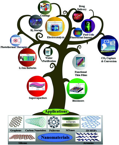
Nanotechnology is an excellent example of an emerging technology, offering engineered nanomaterials with the great potential for producing products with substantially improved performances.13 Currently, nanomaterials find commercial roles in scratch-free paints, surface coatings, electronics, cosmetics, environmental remediation, sports equipment, sensors, and energy-storage devices.14 This review attempts to provide information in a single platform about the basic concepts, advances, and trends relating to nanomaterials via covering the related information and discussing synthesis methods, properties, and possible opportunities relating to the broad and fascinating area of nanomaterials (Scheme 1). It is not easy to cover all the literature related to nanomaterials, but important papers from history and the current literature are discussed in this review. This review provides fundamental insight for researchers, quickly capturing the advances in and properties of various classes of nanomaterials in one place.
2. Descriptions of terms associated with nanomaterials
Rigorous definitions of nanomaterials and associated terms are debatable and still not fixed. For this reason, huge room has been left around the interpretation and classification of nanomaterials. The definition of nanomaterials is not straightforward. In the literature, nanomaterials are perceived in different ways due to the absence of a rigorous definition. Many researchers have used the term nanomaterial if the size is a few nanometers or smaller than a few tens of nanometers, whereas others have even used the term nanomaterial for anything less than a micrometer. The physical and chemical properties of nanomaterials depend upon their precise composition, shape, and size. The effects of nanomaterial on health and the environment also depend upon their size, shape, etc.15 A single internationally accepted definition of nanomaterials is challenging to find,16 and a rigorous definition of nanomaterials is still under discussion in the scientific community. Definitions and descriptions of terms associated with nanomaterials are provided in Table 1. However, these terms are not rigorous; instead, they provide a general perception collected from the available literature.| Term | Description | Ref. |
|---|---|---|
| Nanotechnology | Nanotechnology refers to technology at the nanoscale level in which materials, devices, or systems are developed via controlling matter at the nanoscale length to stimulate the unique properties of the material at the nano-level. | 17 |
| Nanomanufacturing | Nanomanufacturing refers to manufacturing at the nanoscale level and accomplished via bottom-up or top-down methods. | 18 |
| Nanoscale | A scale covering 1–100 nm. | 8 |
| Nanomaterial | A material is called a nanomaterial if it has at least one dimension in the nanoscale range of 1–100 nm. | 19 |
| Nano-object | A nano-object is a discrete piece of material with one, two, or three external dimensions in the nanoscale range. | 3 and 20 |
| Nanoparticle | An object or particle is called a nanoparticle when all of its dimensions are in the nanoscale range. | 19 |
| Aspect ratio | The aspect ratio of a nano-object is defined as the ratio of the length of the major axis to the width of the minor axis. | 21 |
| Nanosphere | A nanosphere is a nanoparticle that has an aspect ratio of 1. | 21 |
| Nanorod | The term nanorod is used when the shortest and longest axes have different lengths. Nanorods have a width in the range of 1 to 100 nm and an aspect ratio greater than 1. | 3 and 21 |
| Nanofiber | A nano-object with two dimensions in the nanoscale range and a third dimension that is significantly larger. | 19 |
| Nanowire | Nanowires are analogues to nanorods, but with a higher aspect ratio. | 21 |
| Nanotube | Hollow nanofibers are called nanotubes. | 19 |
| Nanostructured material | This is a term used for materials that have structural elements, molecules, crystallites, or clusters with dimensions in the range of 1–100 nm. | 22 |
| Nanomaterial | A material is called a nanomaterial if it has at least one dimension in the nanoscale range of 1–100 nm. | 19 |
| Engineered nanomaterials | Intentionally produced materials that have one or more dimensions in the order of 100 nm or less are called engineered nanomaterials. | 17 |
| Nanocomposite | Nanocomposites are defined as multicomponent materials with multiple different phase domains, in which at least one of the phases has at least one dimension in the order of nanometers. | 23 |
3. Approaches for the synthesis of nanomaterials
Two main approaches are used for the synthesis of nanomaterials (Fig. 1): top-down approaches and bottom-up approaches.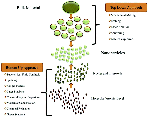 | ||
| Fig. 1 The synthesis of nanomaterials via top-down and bottom-up approaches. Reprinted with permission from ref. 24. Copyright: ©2019, Elsevier B.V. All rights reserved. | ||
3.1. Top-down approaches
In top-down approaches, bulk materials are divided to produce nanostructured materials. Top-down methods include mechanical milling, laser ablation, etching, sputtering, and electro-explosion.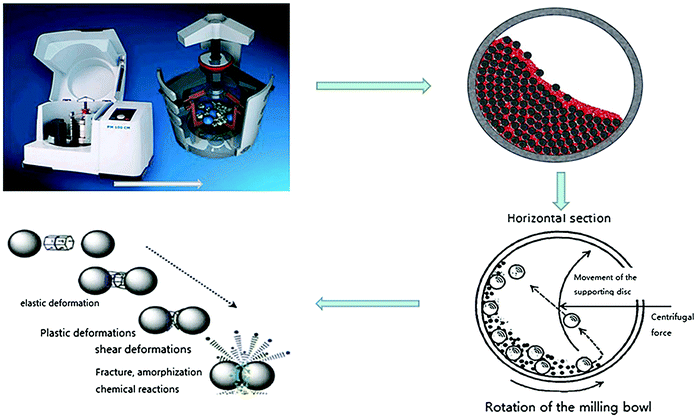 | ||
| Fig. 2 The principle of the ball milling method. Reprinted with permission from ref. 25. Copyright: ©2016, John Wiley & Sons, Ltd. | ||
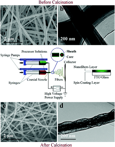 | ||
| Fig. 3 A schematic diagram of the coaxial electrospinning technique (center), and FESEM (a and c) and TEM (b and d) images of fibers before and after calcination. Reprinted with permission from ref. 30. Copyright: ©2012, Elsevier Ltd. All rights reserved. | ||
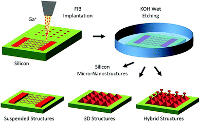 | ||
| Fig. 4 A schematic diagram of the fabrication of 3D micro-nanostructures with an ion beam through bulk Si structuring. This involves implantation in Si through Ga FIB lithography and mask-writing at nanometer resolution, subsequent anisotropic wet etching in KOH solution, and the fabrication of Si micro-nanostructures via the selective removal of the unimplanted region. Reprinted with permission from ref. 37. Copyright: ©2020, Elsevier B.V. All rights reserved. | ||
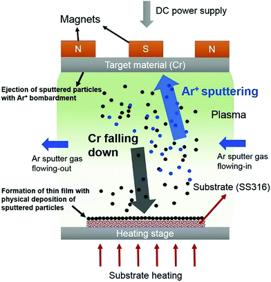 | ||
| Fig. 5 A schematic diagram of the DC magnetron sputtering process. Reprinted with permission from ref. 39. Copyright: ©2017, Elsevier Ltd. All rights reserved. | ||
The conditions under which arc discharge takes place play a significant role in achieving new forms of nanomaterials. The conditions under which different carbon-based nanomaterials are formed via the arc discharge method are explained in Fig. 6. Various carbon-based nanomaterials are collected from different positions during the arc discharge method, as their growth mechanisms differ.44 MWCNTs, high-purity polyhedral graphite particles, pyrolytic graphite, and nano-graphite particles can be collected from either anode or cathode deposits or deposits at both electrodes.46–48 Apart from the electrodes, carbon-based nanomaterials can also be collected from the inner chamber. Different morphologies of single-wall carbon nanohorns (SWCNHs) can be obtained under different atmospheres. For example, ‘dahlia-like’ SWCNHs are produced under an ambient atmosphere, whereas ‘bud-like’ SWCNHs are generated under CO and CO2 atmospheres.49 The arc discharge method can be used to efficiently achieve graphene nanostructures. The conditions present during the synthesis of graphene can affect its properties. Graphene sheets prepared via a hydrogen arc discharge exfoliation method are found to be superior in terms of electrical conductivity and have good thermal stability compared to those obtained via argon arc discharge.50
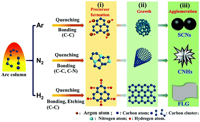 | ||
| Fig. 6 A schematic illustration of the formation mechanisms of carbon nanomaterials on the inner wall of the chamber using different gases via a DC arc discharge approach. Reprinted with permission from ref. 44. Copyright: ©2018, Elsevier Ltd. All rights reserved. | ||
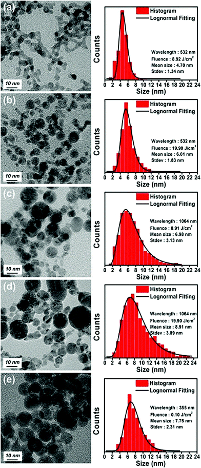 | ||
| Fig. 7 TEM images, corresponding mean sizes, and standard deviations of palladium nanoparticles synthesized via laser ablation in water for 10 min at laser wavelengths and fluences of (a) 532 nm and 8.92 J cm−2, (b) 532 nm and 19.90 J cm−2, (c) 1064 nm and 8.92 J cm−2, (d) 1064 nm and 19.90 J cm−2, and (e) 355 nm and 0.10 J cm−2. Reprinted with permission from ref. 57. Copyright: ©2017, Wiley-VCH Verlag GmbH & Co. KGaA, Weinheim. | ||
3.2. Bottom-up approaches
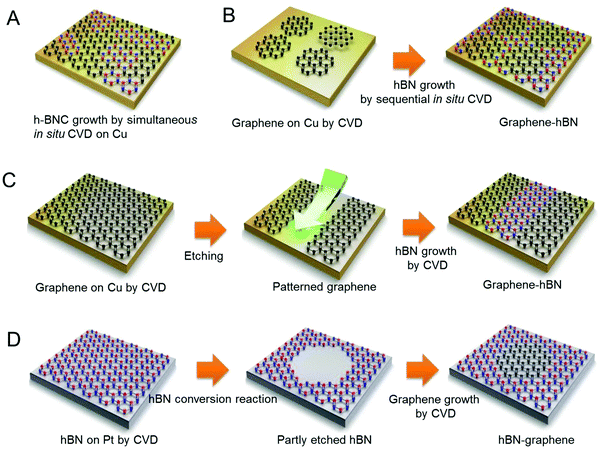 | ||
| Fig. 8 A schematic diagram of the growth of in-plane graphene and hBN heterostructures via various techniques: (A) simultaneous in situ CVD growth, (B) sequential in situ CVD growth, (C) lithography-assisted growth, and (D) conversion growth. Reprinted with permission from ref. 62. Copyright: ©2016, Elsevier B.V. All rights reserved. | ||
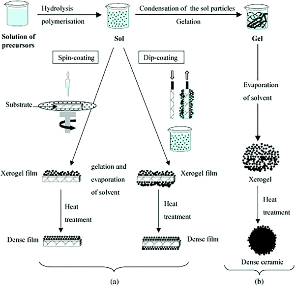 | ||
| Fig. 9 An overview showing two sol–gel method synthesis examples: (a) films from a colloidal sol and (b) powder from a colloidal sol transformed into a gel. Reprinted with permission from ref. 74. Copyright: ©2010, Elsevier B.V. All rights reserved. | ||
The hard template method is also called nano-casting. Well-designed solid materials are used as templates, and the solid template pores are filled with precursor molecules to achieve nanostructures for required applications (Fig. 10).78 The selection of the hard template is critical for developing well-ordered mesoporous materials. It is desirable that such hard templates should maintain a mesoporous structure during the precursor conversion process, and they should be easily removable without disrupting the produced nanostructure. A range of materials has been used as hard templates, not limited to carbon black, silica, carbon nanotubes, particles, colloidal crystals, and wood shells.85 Three main steps are involved in the synthetic pathway for obtaining nanostructures via templating methods. In the first step, the appropriate original template is developed or selected. Then, a targeted precursor is filled into the template mesopores to convert them into an inorganic solid. In the final step, the original template is removed to achieve the mesoporous replica.86Via using mesoporous templates, unique nanostructured materials such as nanowires, nanorods, 3D nanostructured materials, nanostructured metal oxides, and many other nanoparticles can be produced.87 From this brief discussion, it can be seen that a wide range of unique structured nanomaterials can be produced using soft and hard template methods.
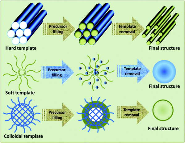 | ||
| Fig. 10 A schematic representation of the synthesis of materials using different types of templates.78 Published by The Royal Society of Chemistry. | ||
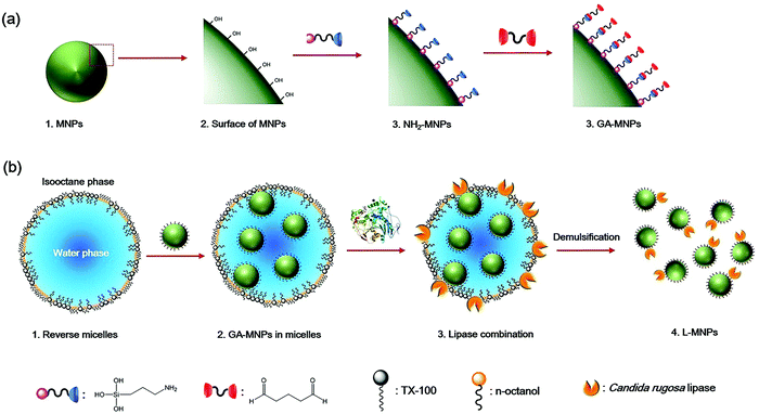 | ||
| Fig. 11 (a) A schematic diagram showing the synthetic steps to GA-MNPs. (b) The synthesis of L-MNPs through a non-ionic reverse micelle method.91 | ||
4. Unique nanomaterial features
The properties of matter at the nanoscale level are substantially distinct compared to bulk counterparts. Size-dependent effects become more prominent at the nanoscale. For example, Au solution appears yellow when in the bulk and it appears purple or red at the nanoscale level. The properties of nanomaterials can be tuned via tuning the nanomaterial size.92,93 At the nanoscale, the electronic properties are substantially changed compared to bulk materials. For example, boron in bulk form is not considered a metal, whereas a two-dimensional network of boron (borophene) appears to be an excellent 2D metal.94 Compared to their bulk counterparts, the mechanical properties of nanomaterials are considerably improved due to increases in crystal perfection or reductions in crystallographic defects.95The electronic properties of semiconductors in the 1–10 nm range are controlled by quantum mechanical considerations. Thus, nanospheres with diameters in the range of 1–10 nm are known as quantum dots. The optical properties of nanomaterials such as quantum dots strongly depend upon their shape and size.96 A photogenerated electron–hole pair has an exciton diameter on the scale of 1–10 nm. Thus, the absorption and emission of light by semiconductors could be controlled via tuning the nanoparticle size in this range. However, in the case of metals, the mean free path of electrons is ∼10–100 nm and, due to this, electronic and optical effects are expected to be observed in the range of ∼10–100 nm. The colors of aqueous solutions of metal nanoparticles can be changed via changing the aspect ratio. Aqueous solutions of Ag NPs show different colors at different aspect ratios. A red shift in the absorption band appears with an increase in the aspect ratio (Fig. 12).21
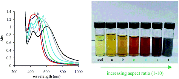 | ||
| Fig. 12 Aqueous solutions of silver nanoparticles show wide variations in visible color depending on the aspect ratio of the suspended nanoparticles. The far left of the photograph shows silver nanospheres (4 nm in diameter) that are used as seeds for subsequent reactions, while (a–f) show silver nanorods with increasing aspect ratios from 1–10. The corresponding visible absorption spectra for (a)–(f) are also shown in the left panel. Reprinted with permission from ref. 21. Copyright: ©2002, WILEY-VCH Verlag GmbH, Weinheim, Fed. Rep. of Germany. | ||
Among a range of unique properties, the following key properties can be obtained upon tuning the sizes and morphologies of nanomaterials.
4.1. Surface area
The surface areas of nanomaterials are generally substantially high compared with their bulk counterparts, and this property is associated with all nanomaterials.974.2. Magnetism
The magnetic behavior of elements can change at the nanoscale. A non-magnetic element can become magnetic at the nanoscale level.934.3. Quantum effects
Quantum effects are more pronounced at the nanoscale level. However, the size at which these effects will appear strongly depends upon the nature of the semiconductor material.984.4. High thermal and electrical conductivity
According to the nature of the nanomaterial, extraordinary thermal and electrical conductivity can be exhibited at the nanoscale level compared to bulk counterparts. One example of this is graphene attained from graphite.994.5. Excellent mechanical properties
Nanomaterials exhibit excellent mechanical properties that are absent in their macroscopic counterparts.1004.6. Excellent support for catalysts
2D sheets of various nanomaterials have provided the opportunity for the good dispersion of nanoparticles of active catalyst, enhancing the catalyst performance substantially.101 Recently, catalysts have been atomically dispersed on 2D sheets of nanomaterials to boost performance.1024.7. Antimicrobial activity
Some nanomaterials possess antiviral, antibacterial, and antifungal properties and have an excellent capacity to deal with pathogen-related diseases.103,104Overall, these features have made nanoscale materials valuable for a wide range of applications, substantially boosting the performances of various devices and materials in a number of fields. Details of various nanomaterials, their properties, and applications in various fields will be discussed below.
5. Nanomaterials, characteristics, and applications
5.1. Special carbon-based nanomaterials
The carbon-based nanomaterial family consists of nanomaterials that have been extensively explored for various applications due to their outstanding features. The extraordinary properties of tunable carbon-based nanomaterials have attracted great interest for use in new technologies and addressing modern challenges.105,106 The carbon family consists of several unique nanomaterials, including CNTs, fullerenes, graphene, carbon nanohorns, carbon-based quantum dots, and many others. These nanomaterials are briefly discussed in this section, elaborating on their key characteristics and significance.In the carbon-based nanomaterial family, fullerenes were the first symmetric material, and they provided new perspectives in the nanomaterials field. This led to the discovery of other carbon-based nanostructured materials, such as carbon nanotubes and graphene.110 Fullerenes are present in nature and interstellar space.111 Interestingly, fullerenes were the molecule of the year in 1991 and attracted the most research projects compared to other scientific subjects during that period.112 Fullerenes possess several unique features that make them attractive for applications in different fields. Fullerenes display solubility to some extent in a range of solvents, and these characteristics make them unique compared to the other allotropes of carbon.108
The chemical modification of fullerenes is an exciting subject, improving their effectiveness for applications. There are two main ways to modify fullerenes:113 fullerene inner-space modification, and fullerene outer-surface modification.
Endohedral and exohedral doping examples are shown in Fig. 13.114 Fullerenes are hollow cages, and the interior acts as a robust nano-container for host target species when forming endohedral fullerene.115 Endohedral fullerenes do not always follow the isolated pentagon rule (IPR).116 To date, fullerene nanocages have received substantial consideration in the materials chemistry field due to their useful potential applications. Neutral and charged single atoms in free space are highly reactive and unstable. In the confined environment of fullerenes, these reactive species can be stabilized; for example, the LaC60+ ion does not react with the NH3, O2, H2, or NO. Thus, reactive metals can be protected from the surrounding environment by trapping them inside fullerene cages.117 Another emerging carbon nanomaterial is endohedral fullerene containing lithium (Li@C60).118 Lithium metal is very reactive, and extreme controlled environmental conditions are required to preserve or use it. In other words, secure structures are required for lithium storage. Li-Based endohedral fullerene shows unique solid-state properties. The encapsulation of lithium atoms in fullerene helps to protect lithium atoms from external agents. Li-Based endohedral fullerenes have the potential to open the door to nanoscale lithium batteries.119 For the development of endohedral metallofullerenes, larger fullerenes are generally required, as they possess large cages to accommodate lanthanide and transition metal atoms more smoothly.118 Fullerene nanocages are useful for the storage of gases. Fullerene is under consideration for hydrogen storage.120,121
 | ||
| Fig. 13 A schematic representation of the two interstitial doping sites in C60, leading to exohedral and endohedral doping. Reprinted with permission from ref. 114. Copyright: ©2009, WILEY-VCH Verlag GmbH & Co. KGaA, Weinheim. | ||
Exohedral fullerenes carry more potential for applications as outer surfaces can be more easily modified or functionalized. The exohedral doping of metals into fullerenes strongly affects the electronic properties via shifting electrons from the metal to the fullerene nanocage.122 The practical application of fullerenes can be achieved with tailor-made fullerene derivatives via chemical functionalization. As fullerene chemistry has matured, a wide range of functionalized fullerenes has been realized through simple synthetic routes.123 The combination of hydrogen-bonding motifs and fullerenes has allowed the modulation of 1D, 2D, and 3D fullerene-based architectures.124 The excellent electron affinities of fullerenes have shown great potential for eliminating reactive oxygen species. The presence of excess reactive oxygen species can cause biological dysfunction or other health issues. The surfaces of fullerenes have been functionalized via mussel-inspired chemistry and Michael addition reactions for the fabrication of C60–PDA–GSH. The developed C60–PDA–GSH nanoparticles demonstrated excellent potential for scavenging reactive oxygen species.125
Amphiphiles have great importance in industrial processes and daily life applications. Amphiphilic molecules consist of hydrophilic and hydrophobic parts, and they perform functions in water via forming two- and three-dimensional assemblies. Recently, conical fullerene amphiphiles126 have emerged as a new class of amphiphiles, in which a nonpolar apex is supplied by fullerenes and a hydrophilic part is achieved through functionalization. The selective functionalization of the fullerene on one side helps to achieve a supramolecule due to unique interfacial behavior. The unique supramolecular structure formed via the spontaneous assembly of one-sided selectively functionalized fullerenes through strong hydrophobic interactions between the fullerene apexes and polar functionalized portions is soluble in water. Conical fullerene amphiphiles are mechanically robust. Via upholding the structural integrity, conical fullerene amphiphiles can be readily aggregated with nanomaterials and biomolecules to form multicomponent agglomerates with controllable structural features.127 Fullerenes, after suitable surface modification, have excellent potential for use in drug delivery, but there have only been limited explorations of their drug delivery applications.128,129 Fullerene-based nano-vesicles have been developed for the delayed release of drugs.130 Water-soluble proteins have great potential in the field of nanomedicine. The water-soluble cationic fullerene, tetra(piperazino)[60] fullerene epoxide (TPFE), has been used for the targeted delivery of DNA and siRNA specifically to the lungs.131 For diseases in lungs or any other organ, efficient treatment requires the targeted delivery of active agents to a targeted place in the organ. The accumulation of micrometer-sized carriers in the lung makes lung-selective delivery difficult, as this may induce embolization and inflammation in the lungs. Size-controlled blood vessel carrier vehicles have been developed using tetra(piperazino)fullerene epoxide (TPFE). TPFE and siRNA agglutinate in the bloodstream with plasma proteins and, as a result, micrometer-sized particles are formed. These particles clog the lung capillaries and release siRNA into lungs cells; after siRNA delivery, they are immediately cleared from the lungs (Fig. 14).132
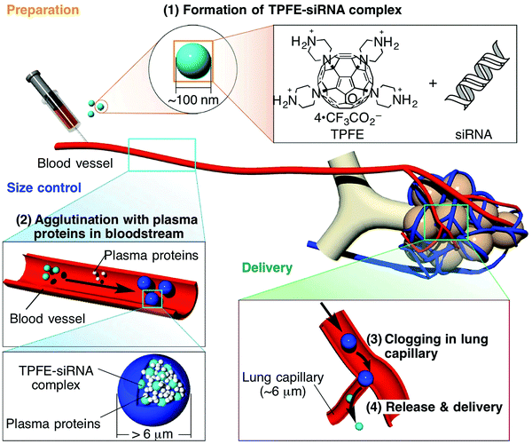 | ||
| Fig. 14 The mechanism of the lung-specific delivery of siRNA mediated by tetra(piperazino)fullerene (TPFE): (1) TPFE aggregates with siRNA to form ca. 100 nm-sized TPFE–siRNA complexes (light blue particles) via electrostatic interactions; (2) the complexes agglutinate with plasma proteins (white particles) in the bloodstream to form >6 μm particles (blue particles); (3) the particles clog and accumulate in the narrow lung capillaries; (4) the TPFE–siRNA complexes were delivered into lung cells and siRNA was released into lung cells. Reprinted with permission from ref. 132. Copyright: ©2014, Springer Nature. | ||
The supramolecular organization of fullerene (C60) is a unique approach for producing shape-controlled moieties on the nano-, micro-, and macro-scale. Nano-, micro-, and macro-scale supramolecular assemblies can be controlled via manipulating the preparation conditions to achieve unique optoelectronic properties.133 The development of well-ordered and organized 1D, 2D, and 3D fullerene assemblies is essential for achieving advanced optical and organic-based electronic devices.134 Fullerene-based nanostructured materials with new dimensions are being developed from zero-dimensional fullerene and tuned to achieve the desired characteristics. 1D C60 fullerene nanowires have received substantial attention over other crystalline forms due to their excellent features of potential quantum confinement effects, low dimensionality, and large surface areas.135
Carbon nanomaterials are also used as supports for catalysts, and the main reasons to use them are their high surface areas and electrical conductivities. Carbon supports strongly influence the properties of metal nanoparticles. In fuel cells, the carbon support strongly affects the stability, electronic conductivity, mass transport properties, and electroactive surface area of the supported catalyst.136 In fuel cells, the degradation of some catalysts, such as platinum-based examples, and carbon is correlated and reinforced as a result of both being present. Carbon support oxidation is catalyzed by platinum and the oxidation of carbon accelerates platinum-catalyst release. Overall, this results in a loss of catalytically active surface area.137 Fullerenes are considered suitable support materials due to their excellent electrochemical activities and stability during electrochemical reactions.138 Due to their high stability and good conductivity, fullerenes can replace conventional carbon as catalyst support materials. Fullerenes are also used for the development of efficient solar cells.139
Apart from the applications mentioned above, fullerenes have a broader spectrum of applications where they can be used to improve outcomes considerably. Fullerenes have the potential to be used in the development of superconductors.140 The strong covalent bonds in fullerenes make them useful nanomaterials for improving the mechanical properties of composites.141 The combination of fullerenes with polymers can result in good flame-retardant and thermal properties.142 Fullerenes and their derivatives are used for the development of advanced lubricants. They are used as modifiers for greases and individual solid lubricants.138 Fullerenes have tremendous medicinal importance due to their anticancer, antioxidant, anti-bacterial, and anti-viral activities.104
Fullerenes are vital members of the carbon-based nanomaterial family and they certainly possess exceptional properties. This discussion further emphasizes their importance for advanced applications. However, the discovery of other carbon-based nanomaterials has put fullerenes in the shade, and the pace of their exploration has been reduced. As fullerenes are highly symmetrical molecules with unique properties, they can act as performance boosters, but more attention is needed from researchers for their practical expansion.110
Single-walled carbon nanotubes consist of a seamless one-atom-thick graphitic layer, in which carbon atoms are connected through strong covalent bonds.146 Double-walled carbon nanotubes consist of two single-walled carbon nanotubes. One carbon nanotube is nested in another nanotube to construct a double-walled carbon nanotube.147 In multi-walled carbon nanotubes, multiple sheets of single-layer carbon atom are rolled up. In other words, many single-walled carbon nanotubes are nested within each other. From different types of nanotubes, it can be concluded that the nanotubes may consist of one, tens, or hundreds of concentric carbon shells, and these shells are separated from each other with a distance of ∼0.34 nm.148 Carbon nanotubes can be synthesized via chemical vapor deposition,149 laser ablation,150 arc-discharge,143 and gas-phase catalytic growth.151
Single-walled carbon nanotubes display a diameter of 0.4 to 2 nm. The inner wall distance between double-walled carbon nanotubes was found to be in the range of 0.33 to 0.42 nm. MWCNT diameters are usually in the range of 2–100 nm, and the inner wall distance is about 0.34 nm.147,152 However, it is essential to note that the diameters and lengths of carbon nanotubes are not well defined, and they depend on the synthesis route and many other factors. The electrical conductivities of SWCNTs and MWCNTs are about 102–106 S cm−1 and 103–105 S cm−1, respectively. SWCNTs and MWCNTs also display excellent thermal conductivities of ∼6000 W m−1 K−1 and ∼2000 W m−1 K−1, respectively. CNTs remain stable in air at temperatures higher than 600 °C.153 These properties indicate that CNTs have obvious advantages over graphite.
Single-walled carbon nanotubes can display metallic or semiconducting behavior. Whether carbon nanotubes show metallic or semiconducting behavior depends on the diameter and helicity of the graphitic rings.154 The rolling of graphene sheets leads to three different types of CNTs: chiral, armchair, and zigzag (Fig. 15).155
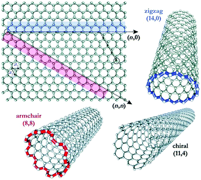 | ||
| Fig. 15 The rolling up of a graphene sheet leading to the three different types of CNT. Reprinted with permission from ref. 155. Copyright: ©2005, WILEY-VCH Verlag GmbH & Co. KGaA, Weinheim. | ||
Carbon nanotubes demonstrate some amazing characteristics that make them valuable nanomaterials for possible practical applications. Theoretical and experimental studies of carbon nanotubes have revealed their extraordinary tensile properties. J. R. Xiao et al. used an analytical molecular structural mechanics model to predict SWCNT tensile strengths of 94.5 (zigzag nanotubes) and 126.2 (armchair nanotubes) GPa.156 In another study, the Young's modulus and average tensile strength of millimeter-long multi-walled carbon nanotubes were analyzed and found to be 34.65 GPa and 0.85 GPa, respectively.157 Carbon nanotubes possess a high aspect ratio. Due to their high tensile strength, carbon nanotubes are used to enhance the mechanical properties of composites.
Carbon nanotubes have become an important industrial material and hundreds of tonnes are produced for applications.158 Their high tensile strength and high aspect ratio have made carbon nanotubes an ideal reinforcing agent.159 Carbon nanotubes are lightweight in nature and are used to produce lightweight and biodegradable nanocomposite foams.160 The structural parameters of carbon nanotubes define whether they will be semiconducting or metallic in nature. This property of carbon nanotubes is considered to be effective for their use as a central element in the design of electronic devices such as rectifying diodes,161 single-electron transistors,162 and field-effect transistors.163 The chemical stability, nano-size, high electrical conductivity, and amazing structural perfection of carbon nanotubes make them suitable for electron field emitter applications.164 The unique set of mechanical and electrochemical properties make CNTs a valuable smart candidate for use in lithium-ion batteries.165 CNTs have the full potential to be used as a binderless free-standing electrode for active lithium-ion storage. CNT-based anodes can have reversible lithium-ion capacities exceeding 1000 mA h g−1, and this is a substantial improvement compared with conventional graphite anodes. In short, the following factors play a role in controlling and optimizing the performances of CNT-based composites:166 (i) the volume fraction of carbon nanotubes; (ii) the CNT orientation; (iii) the CNT matrix adhesion; (iv) the CNT aspect ratio; and (iv) the composite homogeneity.
For some applications, a proper stable aqueous dispersion of CNTs at a high concentration is pivotal to allow the system to perform its function efficiently and effectively.167 One of the major issues associated with carbon nanotubes is their poor dispersion in aqueous media due to their hydrophobic nature. Clusters of CNTs are formed due to van der Waals attraction, π–π stacking, and hydrophobicity. The CNT clusters, due to their strong interactions, hinder solubility or dispersion in water or even organic-solvent-based systems.168 This challenging dispersion associated with CNTs has limited their use for promising applications, such as in biomedical devices, drug delivery, cell biology, and drug delivery.167 Carbon nanotube applications and inherent characteristics can be further tuned via suitable functionalization. The functionalization of carbon nanotubes helps scientists to manipulate the properties of carbon nanotubes and, without functionalization, some properties are not attainable.169 The functionalization of nanotubes can be divided into two main categories: covalent functionalization and non-covalent functionalization.
5.1.1. The covalent functionalization of CNTs. The covalent functionalization of CNTs has substantially improved the utility of nanomaterials for various applications. In covalent functionalization, the functional group is covalently attached to the sidewalls of the carbon nanotubes. Covalent functionalization is generally carried out via two approaches: (1) the activation of the carbon nanotubes by generating reactive species such as hydroxyl groups, amine groups, and carboxylic groups; and (2) the direct covalent attachment of the desired functionalities using radical addition, cycloaddition, and electrophilic and nucleophilic addition reactions.170 Functionalization via the sidewalls and ends/defects are two subcategories of the covalent functionalization of CNTs.171
The heating of CNTs under strongly acidic and oxidative conditions results in the formation of oxygen-containing functionalities. These functional groups, such as carboxylic acid, react further with other functional groups, such as amines or alcohols, to produce amide or ester linkages on the carbon nanotubes.172 One of the main issues preventing the utilization of CNTs for biomedical applications is their toxicity. The cytotoxicity of pristine carbon nanotubes can be reduced via introducing carbonyl, –COOH, and –OH functional groups. Apart from functionalization through oxidized CNTs, the direct functionalization of CNTs is also possible. However, direct functionalization requires more reactive species to directly react with the CNTs, such as free radicals. Addition reactions to CNTs can cause a transformation from sp2 hybridization to sp3 hybridization at the point of addition. At the point where functionalization has taken place, the local bond geometry is changed from trigonal planar to tetrahedral geometry. Some addition reactions to the sidewalls of CNTs are shown in Fig. 16.155
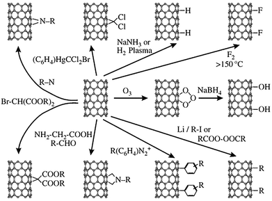 | ||
| Fig. 16 An overview of possible addition reactions for the functionalization of nanotube sidewalls. Reprinted with permission from ref. 155. Copyright: ©2005, WILEY-VCH Verlag GmbH & Co. KGaA, Weinheim. | ||
It is important to discuss how the covalent functionalization of carbon nanotubes comes at the price of the degradation of the carbon sp2 network. This substantially affects the electronic, thermal, and optoelectronic properties of the carbon nanotubes.169 Efforts are being made to introduce a new method of covalent functionalization that can keep the π network of CNTs intact. Antonio Setaro et al. introduced a new [2+1] cycloaddition reaction for the non-destructive, covalent, gram-scale functionalization of single-walled carbon nanotubes. The reaction rebuilds the extended π-network, and the carbon nanotubes retained their outstanding quantum optoelectronic properties (Fig. 17).173
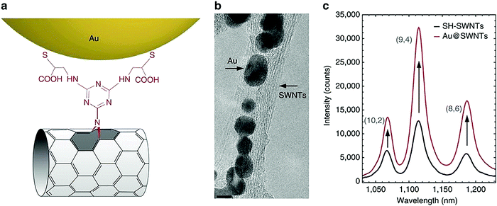 | ||
| Fig. 17 (a) A molecular sketch of AuNPs covalently anchored to SH-SWNTs. (b) A TEM micrograph of the Au@SWNTs hybrid; scale bar: 5 nm; few-SWNT bundles can be observed, and AuNPs are assembled along the tubes. (c) The enhancement of the luminescence emission of SWNTs after the covalent attachment of AuNPs onto their surface: a comparison between the emission of Au@SWNTs hybrid (red curve) and that of SH-SWNTs (black curve). Reprinted with permission from ref. 173. Copyright: ©2017, Springer Nature. | ||
5.1.2. Non-covalent functionalization. The non-covalent modification of CNTs is one of the simplest and most effective ways to functionalize the surface of CNTs to enhance their dispersibility and performance for relevant applications. The non-covalent functionalization of CNTs is achieved using π–π interactions, CH–π interactions, van der Waals attraction, and electrostatic interactions. The non-covalent functionalization of CNTs is considered to be advantageous as it does not involve damaging the sp2 carbon network of CNTs and it helps to preserve the intrinsic characteristics of the CNTs.174 Different materials, such as polymers, aromatic compounds, and head–tail surfactants, are used for non-covalent functionalization.175
Polymers are frequently combined with CNTs to enhance their dispersion capabilities. Polymers interact with CNTs through CH–π and π–π interactions.174 Hexanes and cycloalkanes are poor CNT solvents but the good solubility or dispersion of CNTs in these solvents is required for surface coating applications. Poly(dimethylsiloxane) (PDMS) macromer-grafted polymers have been prepared using PDMS macromers and pyrene-containing monomers that strongly adsorb on CNTs, thus improved the solubility of CNTs in chloroform and hexane.176 The use of head–tail surfactants is another attractive way to achieve a fine dispersion of CNTs in an aqueous medium. In head–tail surfactants, the tail is hydrophobic and interacts with the CNT sidewalls, and the hydrophilic head groups interact with the aqueous environment to provide a fine dispersion.177
For electrical applications, non-covalently functionalized CNTs are more preferred because the electrical properties of the CNTs are not compromised. CNTs have been non-covalently functionalized with a variety of biomolecules for the fabrication of electrochemical biosensors.175 Non-covalently functionalized SWCNTs are used for energy applications. Single-walled carbon nanotubes (SWCNTs) have been non-covalently functionalized with 3d transition metal(II) phthalocyanines, lowering the potential of the oxygen evolution reaction by approximately 120 mV compared with unmodified SWCNTs.178 The toxicity of pristine CNTs toward living organisms can be lessened via using surfactant-functionalized CNTs.170 However, in some cases, during polymer non-covalent functionalization, the polymer may wrap CNT bundles and make it difficult to separate the CNTs from each other. Polymers can develop into insulating wrapping that affects the CNT conductivity.
![[thin space (1/6-em)]](https://www.rsc.org/images/entities/char_2009.gif) 000 cm2 V−1 s−1 at electron densities of ∼2 × 1011 cm−2via suspending single-layer graphene.186 The distinctive properties of graphene have attracted significant attention from researchers. They have started to evaluate it theoretically and experimentally in order to boost the performances of various devices via overcoming conventional challenges (Table 2).
000 cm2 V−1 s−1 at electron densities of ∼2 × 1011 cm−2via suspending single-layer graphene.186 The distinctive properties of graphene have attracted significant attention from researchers. They have started to evaluate it theoretically and experimentally in order to boost the performances of various devices via overcoming conventional challenges (Table 2).
| Term | Pristine graphene | Graphene oxide | Reduced graphene oxide | Ref. |
|---|---|---|---|---|
| Definition | A single layer of 2D carbon atoms | Heavily oxidized graphene | A reduced form of graphene oxide | 191 |
| Composition | Consists of carbon atoms | Consists of C, O, and H | Consists of C, O, and H | |
| C/O ratio | No oxygen | 2–4 | Depends upon the synthesis process; contains less oxygen (8–246) | 192 |
| Hybridization | sp2 | sp2 and sp3 | Predominantly sp2 and slightly sp3 | 193 |
| Defects | Defect-free | Defects present | Defects present | 194 |
| Preparation | Relatively tough | Easy | Easy | 195 |
| Production cost | High | Low | Low | 192 |
| Electrical conductivity | Highest | Poor | The electrical properties are partially restored | 188 |
In the literature, several graphene-related materials have been reported, such as graphene oxide and reduced graphene oxide.187 Among graphenoids, graphene oxide is a more reported and explored graphene-related material as a precursor for chemically modified graphene. The synthetic route to graphene oxide is straightforward, and it is synthesized from inexpensive graphite powder that is readily available.188 Graphene oxide has many oxygen-containing functional groups, such as epoxy, hydroxyl, carboxyl, and carbonyl groups. The basal plane of graphene oxide is generally decorated with epoxide and hydroxyl groups, whereas the edges presumably contain carboxyl- and carbonyl-based functional groups.189 The presence of active functional groups in graphene oxide allows its further functionalization with different polymers, small organic compounds, or other nanomaterials to realize several applications.190
Graphene oxide, due to its oxygen functionality, is insulating in nature and displays poor electrochemical performance. The presence of oxygen functionalities in graphene oxide breaks the conjugated structure and localizes the π-electron network, resulting in poor carrier mobility and carrier concentration.196 Its electrochemical performance is improved substantially after removing the oxygen-containing functional groups.197 These functional groups can be removed or reduced via thermal, electrochemical, and chemical means. The product obtained after removing or reducing oxygen moieties is called reduced graphene oxide. The properties of reduced graphene oxide depend upon the effective removal of oxygen moieties from graphene oxide. The process used to remove oxygen-containing functionalities from graphene oxide will determine the extent to which reduced the properties of graphene oxide resemble pristine graphene.198
Reduced graphene oxide is extensively used to improve the performances of various electrochemical devices.199 It is essential to mention that even after reducing graphene oxide, some residual sp3 carbon bonded to oxygen still exists, which somehow disturbs the movement of charge through the delocalized electronic cloud of the sp2 carbon network.200 Apart from this, the electrochemical activity of reduced graphene oxide is substantially high enough to manufacture electrochemical devices with improved performances. Recently, the demand for super-performance electrochemical devices has increased to overcome modern challenges relating to electronics and energy-storage devices.201 Graphene-based materials are considered to be excellent electrode materials, and they can be proved to be revolutionary for use in energy-storage devices such as supercapacitors (SC) and batteries. Graphene-based electrodes improve the performances of existing batteries (lithium-ion batteries) and they are considered useful for developing next-generation batteries such as sodium-ion batteries, lithium–O2 batteries, and lithium–sulfur batteries (Fig. 18). Being flat in nature, each carbon atom of graphene is available, and ions can easily access the surface due to low diffusion resistance, which provides high electrochemical activity.202
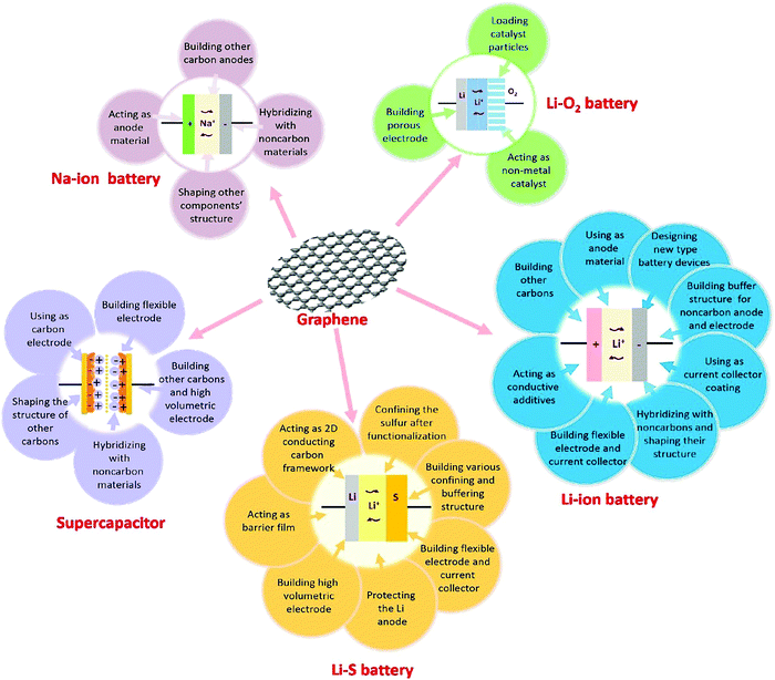 | ||
| Fig. 18 The applications of graphene in different electrochemical energy storage devices (EESDs). Reprinted with permission from ref. 202. Copyright: ©2015, Elsevier B.V. All rights reserved. | ||
Graphene and its derivatives are extensively used for the development of electrochemical sensors.203 The surfaces of bare electrodes are usually not able to sense analytes at trace levels and they cannot differentiate between analytes that have close electrooxidation properties due to their poor surface kinetics. The addition of graphene layers to the surfaces of electrodes can substantially improve the electrocatalytic activity and surface sensitivity towards analytes.204 Graphene has definite advantages over other materials that are used as electrode materials for sensor applications. Graphene has a substantially high surface-to-volume ratio and atomic thickness, making it extremely sensitive to any changes in its local environment. This is an essential factor in developing advanced sensing tools, as all the carbon atoms are available to interact with target species.
Consequently, graphene exhibits higher sensitivity than its counterparts such as CNTs and silicon nanowires.205 Graphene has two main advantages over CNTs for the development of electrochemical sensors. First, graphene is mostly produced from graphite, which is a cost-effective route, and second, graphene does not contain metallic impurities like CNTs can. Graphene offers many other advantages when developing sensors and biosensors, such as biocompatibility and π–π stacking interactions with biomolecules.206 Graphene-based materials are ideal for the construction of nanostructured sensors and biosensors.
The mechanical properties of graphene are used to fabricate highly desired stretchable and flexible sensors.207 Graphene can be utilized to develop transparent electrodes with excellent optical transmittance. It displays good piezoresistive sensitivity. Researchers are making efforts to replace conventional brittle indium tin oxide (ITO) electrodes with flexible graphene electrodes in optoelectronic devices such as liquid-crystal displays and organic light-emitting diodes.208 For human–machine interfaces, transparent and flexible tactile sensors with high sensitivity have become essential. Graphene film (GF) and PET have been applied to develop transparent tactile sensors that exhibit outstanding cycling stability, fast response times, and excellent sensitivity (Fig. 19).209 Similarly, graphene is applied for the fabrication of pressure sensors.210 Overall, graphene is an excellent material for developing transparent and flexible devices.211,212
 | ||
| Fig. 19 (a) A schematic diagram of the fabrication procedure of a tactile sensor based on GF and a PET plate. (b) An optical photograph of a bent assembled sensor; the geometrical dimensions of the sensor are shown in the inset. (c) The Raman spectrum of the GF, with typical D (≈1352 cm−1), G (≈1583 cm−1), and 2D (≈2686 cm−1) peaks. (d) Transmittance spectra of pure PET, the GF–PET composite structure, and a multilayer stacked nanofilm sensor in the visible wavelength range from 350 to 700 nm.209 Published by The Royal Society of Chemistry. | ||
The use of graphene-based materials is an effective way to deal with a broad spectrum of pollutants.213 There are many ways to deal with environmental pollution; among these, adsorption is an effective and cost-effective method.214,215 Graphene-based adsorbents are found to be useful in the removal of organic,216 inorganic, and gaseous contaminants. Graphene-based materials have some obvious advantages over CNT-based adsorbents. For example, graphene sheets offer two basal planes for contaminant adsorption, enhancing their effectiveness as an adsorbent.192 GO contains several oxygen functional groups that impart hydrophilic features. Due to appropriate hydrophilicity, GO-based adsorbents can efficiently operate in water to remove contaminants. Moreover, graphene-oxide-based materials can be functionalized further through reactive moieties with various organic molecules to enhance their adsorption capacities.217
In short, extensive research must continue in order to develop graphene-based materials with high performance and bring them to the market. Massive focus on graphene research is also justified due to the extraordinary features described in extensive theoretical and experimental research works.
Nanodiamonds possess a core–shell-like structure and display rich surface chemistry, and numerous functional groups are present on their surface. Several functional groups, such as amide, aldehyde, ketone, carboxylic acid, alkene, hydroperoxide, nitroso, carbonate ester, and alcohol groups, are present on nanodiamond surfaces, assisting in their further functionalization for desired applications (Fig. 20).226
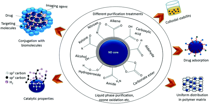 | ||
| Fig. 20 The critical surface chemistry of detonation-based NDs. The ND surface is usually covered with several functional groups. Different surface treatments (such as liquid phase purification and ozone oxidation) are needed to replace these functional groups with oxygen-containing species like carboxylic acids and anhydrides. Surface-treated NDs exhibit several attractive properties, such as colloidal stability, drug adsorption, uniform distribution in a polymer matrix, conjugation with biomolecules, and catalytic properties. Reprinted with permission from ref. 226. Copyright: ©2018, Elsevier Ltd. All rights reserved. | ||
Furthermore, nanodiamond surfaces can be homogenized with a single type of functional group according to the application requirements.227 The use of nanodiamond particles as a reinforcing material in polymer composites has attracted great attention for improving the performance of polymer composite materials. The superior mechanical properties and rich surface chemistry of nanodiamonds have made them a superior material for tuning and reinforcing polymer composites. Nanodiamonds might operate via changing the interphase properties and forming a robust covalent interface with the matrix.228 Nanodiamond (ND)-reinforced polymer composites have shown superior thermal stabilities, mechanical properties, and thermal conductivities. Nanodiamonds have shown great potential for energy storage applications.229 Nanodiamonds and their composites are also used in sensor fabrication, environmental remediation, and wastewater treatment.230,231 Their stable fluorescence and long fluorescence lifetimes have made nanodiamonds useful for imaging and cancer treatment. For biomedical applications, the rational engineering of nanodiamond particle surfaces has played a crucial role in the carrying of bioactive substances, target ligands, and nucleic acids, resisting their aggregation.232,233 Nanodiamonds have a great future in nanotechnology due to their amazing surface chemistry and unique characteristics.
Carbon quantum dots can be synthesized through several chemical routes.241–245 Some methodologies for synthesizing carbon dots are described in Fig. 21.246–248 Carbon itself is a black material and displays low solubility in water. In contrast, carbon quantum dots are attractive due to their excellent solubility in water. They contain a plethora of oxygen-containing functional groups on their surface, such as carboxylic acids. These functional moieties allow for further functionalization with biological, inorganic, polymeric, and organic species.
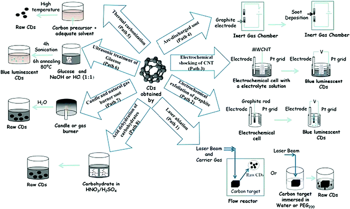 | ||
| Fig. 21 Methodologies for synthesizing carbon dots (CDs). Reprinted with permission from ref. 246. Copyright: ©2011, Elsevier Ltd. All rights reserved. | ||
Carbon quantum dots are also called carbon nano-lights due to their strong luminescence.248 In particular, carbon quantum dots offer enhanced chemiluminescence,249,250 fluorescent emission,251 two-photon luminescence under near-infrared pulsed-laser excitation,252 and tunable excitation-dependent fluorescence.253 The luminescence characteristics of carbon quantum dots have been used to develop highly sensitive and selective sensors. In most cases, a simple principle is involved in sensing with luminescent carbon quantum dots: their photoluminescence intensity changes upon the addition of an analyte.254 Based on this principle, several efficient sensors have been developed using carbon quantum dots.255–257 They can be used as sensitive and selective tools for sensing explosives such as TNT. Recognition molecules on the surfaces of carbon quantum dots can help to sense targeted analytes. Amino-group-functionalized carbon quantum dot fluorescence is quenched in the presence of TNT through a photo-induced electron-transfer effect between TNT and primary amino groups. This quenching phenomenon can help to sense the target analyte (Fig. 22).258 Chiral carbon quantum dots (cCQDs) can exhibit an enantioselective response. The PL responses of cCQDs were evaluated toward 17 amino acids and it was found that the PL intensity of the cCQDs was only substantially enhanced in the presence of L-Lys (Fig. 22).254
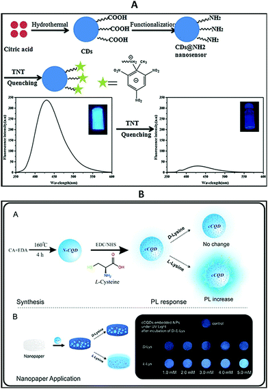 | ||
| Fig. 22 (A) A schematic illustration of the fabrication of a CDs@NH2 nanosensor and its sensing mechanism toward TNT.258 (B) A schematic diagram of the synthesis and application procedures of cCQDs. Reprinted with permission from ref. 254. Copyright: ©2018, Elsevier B.V. All rights reserved. | ||
Carbon quantum dots have received significant interest in the fields of biological imaging and nanomedicine (Fig. 23).239 Direct images of RNA and DNA are essential for understanding cell anatomy. Due to the limitations of current imaging probes, tracking the dynamics of these biological macromolecules is not an easy job. Recently, membrane-penetrating carbon quantum dots have been developed for the imaging of nucleic acids in live organisms.259 It is important to note that most of the carbon quantum dots utilized to attain cell imaging under UV excitation emit blue radiation. Some biological tissue also emits blue light, specifically that involving carbohydrates, and this interferes with cell imaging carried out with blue-emitting CQDs. This seriously hinders their potential in the field of biomedical imaging. Due to this reason, researchers are focusing on tuning CQDs in a way that their emission peak is red-shifted to avoid interference.260 Carbon quantum dots with yellow and green fluorescence have been reported for bioimaging purposes.261,262 The suitable doping of carbon quantum dots can red-shift the emission to enhance the bioimaging effectiveness.263 Doped carbon quantum dots are capable of biological imaging and display advanced capabilities for scavenging reactive oxygen species.264
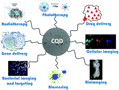 | ||
| Fig. 23 The applications of CQDs in nanomedicine. Reprinted with permission from ref. 239. Copyright: ©2019, Elsevier B.V. All rights reserved. | ||
Carbon quantum dots demonstrate photo-induced electron transfer properties265 that make them valuable for photocatalytic, light-energy conversion, and other related applications.266 Carbon quantum dots enhance the activities of other photocatalysts to which they are attached. Carbon quantum dots, along with photocatalysts, provide better charge separation and suppress the regeneration of photogenerated electron–hole pairs. Moreover, the proper implantation of carbon quantum dots into photocatalysts can broaden the photo-absorption region. Implanted carbon quantum dots form micro-regional heterostructures that facilitate photo-electron transport.267 The implantation of carbon quantum dots into g-C3N4 can substantially enhance charge transfer and separation efficiencies, prevent photoexcited carrier recombination, narrow the bandgap, and red shift the absorption edge.268 The intrinsic catalytic activity of polymeric carbon nitride is improved as a result of the nano-frame heterojunctions formed with the help of CQDs.269
Carbon quantum dots offer many advantages over conventional semiconductor-based QDs and, thus, they have attracted considerable researcher attention.244 Due to their remarkable features, they have shown importance in recent years in the fields of light-emitting diodes, nanomedicine, solar cells, sensors, catalysis, and bioimaging.236
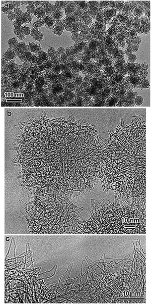 | ||
| Fig. 24 (a) A TEM micrograph showing a graphitic carbon product that was generated abundantly upon CO2 laser ablation at room temperature. The product consisted of near-uniform-sized spherical particles with a diameter of 80 nm. (b) A magnified TEM micrograph of the graphitic carbon particles showing aggregations of tubule-like structures sticking out of the particle surface. (c) A highly magnified TEM micrograph of the edge regions of graphitic particles showing conical horn-like protrusions that are up to 20 nm-long on the particle surface with some modified shapes. Each of these carbon nanohorns was made of a single graphene sheet with closed caps, and the diameters were similar to those of fullerene molecules. Reprinted with permission from ref. 272. Copyright: ©1999, Elsevier Science B.V. All rights reserved. | ||
The production of carbon nanohorns has some obvious advantages over carbon nanotubes, such as the ability for toxic-metal-catalyst-free synthesis and large-scale production at room temperature. Carbon nanotube synthesis involves metal particles, and harsh conditions, such as the use of strong acids, are required to remove metallic catalysts. This process introduces many defects into CNT structures and may cause a loss of carbon material.270 Carbon nanohorns possess a wide diameter compared to CNTs. CNHs possess good absorption capabilities and their interiors are also available after partial oxidation, which provides direct access to their internal parts. Heat treatment under acidic or oxidative conditions facilitates the facile introduction of holes into carbon nanohorns. Holes in graphene sheets of single-walled carbon nanohorns can be produced with O2 gas at high temperatures. A large quantity of material can be stored inside CNH tubes.274 The surface area of CNHs is substantially enhanced upon opening the horns to make their interiors accessible.275 Carbon nanohorns have great potential for energy storage,275 electrochemiluminescence,276 adsorption,277 catalyst support,278 electrochemical sensing,279 and drug delivery system273 uses. CNHs as catalyst supports can provide a homogeneous dispersion of Pt nanoparticles (Fig. 25). The current density of Pt supported on single-walled carbon nanohorns is double compared to a fuel cell made from Pt supported on carbon black.280 Thus, carbon nanohorns provide a better uniform dispersion that facilitates a high surface area and better catalyst performance.
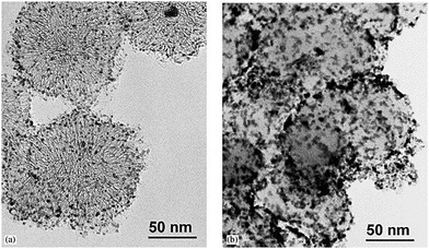 | ||
| Fig. 25 TEM micrographs of a Pt catalyst supported on SWNHs (a) and on carbon black (b). Reprinted with permission from ref. 280. Copyright: ©2002, Elsevier Science B.V. All rights reserved. | ||
5.2. Nanoporous materials
Explorations and research relating to the development of porous materials have fascinated materials chemists for decades.281 One example of a porous materials is activated charcoal, which has been used for many years.282 The technological and scientific importance of porous solids arises from their ability to interact with ions, atoms, and molecules at their outer surface, while their interior is also accessible. Porous materials are generally defined as nanoporous materials when they have a pore diameter of less than 100 nm.283,284 According to the pore size, porous materials can be divided into three major categories:285,286In nanoporous materials, the size distributions, volumes, and shapes of the pores directly affect the performances of porous materials for particular applications. It has become a hot area of research to develop materials with precisely controlled pores and arrangements. Recent research has focused more on the precise control of the shapes, sizes, and volumes of pores to produce nanoporous materials with high performance. Several state-of-the-art reviews are present in the literature that focus explicitly on the synthesis, properties, advances, and applications of nanoporous materials.85,287–289 Based on the materials used, nanoporous materials can be divided into three main groups: inorganic nanoporous materials; carbonaceous nanoporous materials; and organic polymeric nanoporous materials.
Inorganic nanoporous materials include porous silicas, clays, porous metal oxides, and zeolites. The generation of pores in the material can introduce striking features into the material that are absent in non-porous materials. Nanoporous materials offer rich surface compositions with versatile characteristics. Nanoporous materials exhibit high surface-to-volume ratios. Their outstanding features and nanoporous framework structures have made these materials valuable in the fields of environmental remediation, adsorption, catalysis, sensing, energy conversion, purification, and medicine.284,290
Porous silica is a crucial member of the inorganic nanoporous family. Over the decades, it has generated significant research interest for use in fuel cells, chemical engineering, ceramics, and biomedicine. It is essential to note that specific morphologies and pore size diameters are required for each application, and these can be achieved via tuning during the synthesis process. Nanoporous silica offers two functional surfaces: one is the cylindrical pore surfaces, and the second is the exterior surfaces of the nanoporous silica particles. The surfaces of nanoporous silica can be easily functionalized for the desired applications. The nanoporous silica surface is heavily covered with many silanol groups that act as reactive sites for functionalization (Fig. 26).291,292 For biomedical applications, mesoporous silica has emerged as a new generation of inorganic platform materials compared to other integrated nanostructured materials. Several factors make it a unique material for biomedical applications:293,294 (a) its ordered porous structure; (b) its tunable particle size; (c) its large pore volume and surface area; (d) its biocompatibility; (e) its biodegradation, biodistribution, and excretion properties; and (f) its two functional surfaces. For instance, ordered MCM-48 nanoporous silica was used for the delivery of the poorly soluble drug indomethacin. It has been found that surface modification can control drug release.295 Mesoporous silica-based materials have emerged as excellent materials for use in sustained drug delivery systems (SDDSs), immediate drug delivery systems (IDDSs), targeted drug delivery systems (TDDSs), and stimuli-responsive controlled drug delivery systems (CDDSs). The drug release rate from mesoporous silica can also be controlled via introducing appropriate polymers or functional groups, such as CN, SH, NH2, and Cl. Researchers are currently focusing on developing MSN-based (MSN = mesoporous silica nanoparticle) multifunctional drug delivery systems that can release antitumor drugs on demand in a targeted fashion via minimizing the premature release of the drug (Fig. 27).296
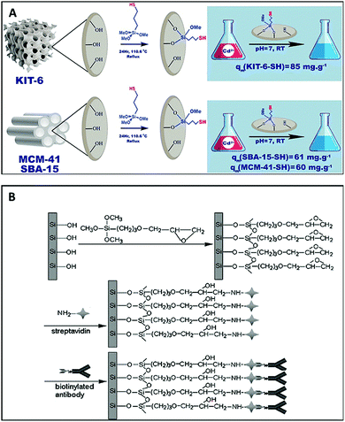 | ||
| Fig. 26 (A) The functionalization of mesoporous silica and the adsorption process of cadmium ions. Reprinted with permission from ref. 292. Copyright: ©2018, Elsevier B.V. All rights reserved. (B) A schematic illustration of the biofunctionalization of 3D nanoporous SiO2 film with streptavidin and antibodies. Reprinted with permission from ref. 291. Copyright: ©2008, WILEY-VCH Verlag GmbH & Co. KGaA, Weinheim. | ||
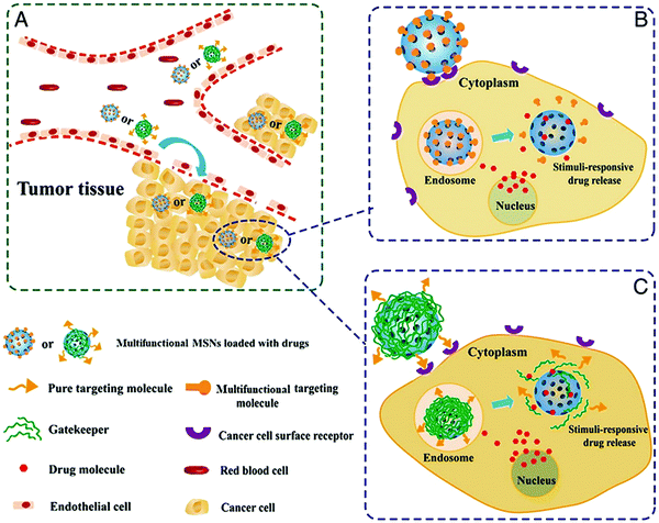 | ||
| Fig. 27 (A) The in vivo process of an MSN-based controlled and targeted drug-delivery system. Two approaches for multifunctional MSN-based drug delivery systems are to design (B) a multifunctional targeting molecule that acts both as a targeting and capping agent or (C) a stimuli-responsive gatekeeper that is further modified with a target moiety to achieve multifunctional drug delivery. Reprinted with permission from ref. 296. Copyright: ©2015, Elsevier Inc. All rights reserved. | ||
Hierarchically nanoporous zeolites are a vital member of the nanoporous material family. They are crystalline aluminosilicate minerals whose structures comprise uniform, regular arrays of nanopores with molecular dimensions. The microporous structures of zeolites contain pores that are usually below 1 nm in diameter. In zeolites, the micropores are uniform in shape and size, and these pores can effectively discriminate between molecules based on shape and size.297 Currently, based on crystallography, more than 200 zeolites have been classified.298 Zeolites have been proved to be useful materials in the field of host–guest chemistry. In solid catalysis, about 40% of the entire solid catalyst field is taken up by zeolites in chemical industry. The excellent catalysis success of zeolites is based on their framework stability, shape-selective porosity, solid acidity, and ion-exchange capacity. Oxygen tetrahedrally coordinates with the Al atoms in most zeolite crystalline silicate frameworks, resulting in charge mismatch between the oxide framework and Al. Extra-framework Na+ ions compensate for this charge mismatch. The Na+ ions are exchangeable for other cations such as H+ and K+.298 The zeolite crystalline networks are remarkable in that they provide high mechanical and hydrothermal stabilities. The most crucial task facing the zeolite community is to find new structures with desired functions and apply them more effectively for different applications.
Apart from these inorganic porous materials, several other metal- and metal-oxide-based nanoporous materials have been introduced that are more prominent for use in electrode material, catalyst, photodegradation, energy storage, and energy conversion applications.299–302 Nanoporous metal-based materials are famous due to the nanosized crystalline walls, interconnected porous networks, and numerous surface metal sites that provide them with unique physical/chemical properties compared with their bulk counterparts and other nanostructured materials.303 For example, nanoporous WO3 films were developed via tuning the anodization conditions for photoelectrochemical water oxidation. It has been observed that the morphology of the film strongly affected the photoelectrochemical performance.304 Nanoporous alumina is also a unique material in the inorganic nanoporous family due to several aspects. Nanoporous alumina can be prepared in a controlled fashion with any size and shape in polyprotic aqueous media via the anodic oxidation of the aluminum surface. The parallel arrangement of pores on alumina can easily be controlled from 5 nm to 300 nm, and alumina is stable in the range of 1000 °C. The anodizing time plays a significant role in controlling the pore length. Nanoporous alumina membranes offer various unique properties, such as pores of variable widths/lengths, temperature stability, and optical transparency. Nanoporous alumina pores can be filled with magnetically and optically active elements to produce the desired applications at the nanoscale level. Photoluminescent alumina membranes can be produced via introducing cadmium sulfide, gallium nitride, and siloxenes inside nanoporous alumina using appropriate precursors.305 Porous alumina also acts as an efficient support and template for the designing of other nanomaterials. Palladium nanowires,306 high aspect ratio cobalt nanowires,307 and highly aligned Cu nanowires308 were developed using porous alumina as a template. Ni–Pd as a catalyst was supported on porous alumina for hydrogenation and oxidation reactions.309 Nanoporous anodic alumina is also considered to be an efficient material for the development of biosensors due to the ease of fabrication, tunable properties, optical/electrochemical properties, and excellent stability in aqueous environments.310
Nanoporous carbon-based materials are a hot topic in the field of materials chemistry. Nanoporous carbon materials have become ubiquitous choices in the environmental, energy, catalysis, and sensing fields due to their unique morphologies, large pore volumes, controlled porous structures, mechanical, thermal, and chemical stabilities, and high specific surface areas (Fig. 28A).311 Nanoporous materials are found to be useful in the treatment of water. The separation of spilled oil and organic pollutants from water has emerged as a significant challenge.312–314 The design of materials that can allow the efficient separation of organic, dye, and metal contaminants from water has become a leading environmental research area.315,316 Nanoporous carbon can be derived from different natural and synthetic sources.317–319 Nanoporous carbon foam can be derived from natural sources, such as flour, pectin, and agar, via table-salt-assisted pyrolysis. The agar-derived nanoporous carbon foam showed high absorption capacities, a maximum of 202 times its own weight, for oil and organic solvents. Air filtration paper developed from carbon nanoporous materials and non-woven fabrics has shown a filtration efficiency of greater than 99% (Fig. 28B).320 Nanoporous carbon can also be produced from other porous frameworks, such as metal–organic frameworks. MOF- and COF-based materials are promising precursors for nanoporous carbon-based materials. The direct carbonization of amino-functionalized aluminum terephthalate metal–organic frameworks has produced nitrogen-doped nanoporous carbon that shows an adequate removal capacity of 98.5% for methyl orange under the optimum conditions.321 Fe3O4/nanoporous carbon was also produced with Fe salts as a magnetic precursor and MOF-5 as a carbon precursor for removing the organic dye methylene blue (MB) from aqueous solutions.322 The mesoporous carbon removal efficiency could be further enhanced via modifying or functionalizing the surface with various materials. Unmodified mesoporous carbon has shown a mercury removal efficiency of 54.5%. This efficiency can be substantially improved to 81.6% and 94% upon modification with the anionic surfactant sodium dodecyl sulfate and cationic surfactant cetyltrimethyl ammonium bromide (CTAB), respectively.323
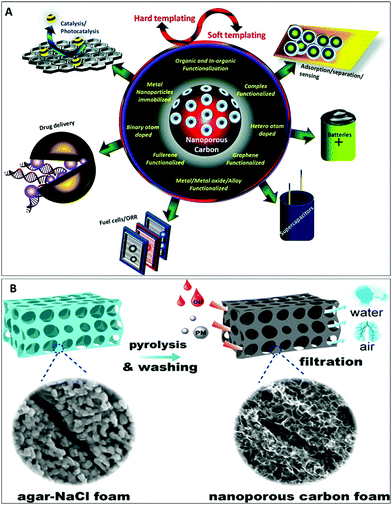 | ||
| Fig. 28 (A) A schematic illustration of the synthesis, functionalization, and applications of micro- and mesoporous carbon. Reproduced from ref. 311 with permission from The Royal Society of Chemistry. (B) The development of nanoporous carbon foam with high efficiency for oil/organic solvent adsorption. Reprinted with permission from ref. 320. Copyright: ©2020, American Chemical Society. | ||
Ordered nanoporous carbon, CNTs, and fullerenes are extensively applied for energy and environmental applications. The complicated synthesis routes required for fullerenes and CNTs have slowed down the full exploitation of their potential for highly demanding applications. In comparison, the synthesis of highly ordered nanoporous carbon is facile, and the properties of ordered nanoporous carbon are also appealing for energy and environmental applications.311 CO2 is a greenhouse gas, and its sustainable conversion into value-added products has become the subject of extensive research. A nitrogen-doped nanoporous-carbon/carbon-nanotube composite membrane is a high-performance gas-diffusion electrode applied for the electrocatalytic conversion of CO2 into formate. A faradaic efficiency of 81% was found for the production of formate.324 Nanoporous carbon materials modified with the non-precious elements P, S, N, and B have emerged as efficient electrode materials for use in the oxygen evolution reaction (OER), hydrogen evolution reaction (HER), oxygen reduction reaction (ORR), batteries, and fuel cells.311,325–327
Nanoporous polymers, including nanoporous coordination polymers and crystalline nanoporous polymers, have emerged as impressive nanoporous materials.328 Nanoporous polymers have many applications, and these materials are extensively being evaluated for gas separation and gas storage. The great interest in these applications arises from the presence of pores providing an exceptionally high Brunauer–Emmett–Teller (BET) surface area. Recently, new classes of metal organic framework and covalent organic framework porous materials have been reported that have shown exceptionally high and unprecedented surface areas. For instance, in 2010, a MOF was reported with a surface area of 6143 m2 g−1;329 in 2012, a MOF was reported with a surface area greater than 7000 m2 g−1;330 and in 2018, a MOF (DUT-60) was reported with a record surface area of 7836 m2 g−1.331 Mesoporous DUT-60 has also shown a high free volume of 90.3% with a density of 0.187 g cm−3.331
Due to their exceptionally high surface areas and porous networks, these MOFs and COFs are ideal for gas storage. Air separation and post-combustion CO2 capture have become integral parts of mainstream industries related to the energy sector in order to avoid substantial economic penalties. Due to the inefficiencies of available technology and the critical importance of this area, earnest efforts are being made to design gas-selective porous materials for the selective adsorption of desired gases. Nanoporous MOF- and COF-based materials can significantly capture CO2 and help reach zero or minimum CO2 emission levels. For instance, nanoporous fluorinated metal–organic frameworks have shown the selective adsorption of CO2 over H2 and CH4.332 Hasmukh A. Patel et al. developed N2-phobic nanoporous covalent organic polymers for the selective adsorption of CO2 over N2. The azo groups in the framework rejected N2, leading to CO2 selectivity.333 Nanoporous polymers that are superhydrophobic in nature can also be used for volatile organic compounds and organic contaminants.334 Nanoporous polymers, due to the presence of a porous network, have been considered as highly suitable materials for catalyst supports. Furthermore, organocatalytic functional groups can be introduced pre-synthetically and post-synthetically into solid catalysts.335
Nanoporous polymeric materials are amazingly heading towards being extremely lightweight with exceptionally high surface areas. These high surface areas and the fine-tuning of the nanopores has made these nanoporous materials, specifically MOFs and zeolites, ideal support materials for encapsulating ultrasmall metal nanoparticles inside void spaces to produce nanocatalysts with exceptionally high efficiencies.336 In the coming years, more exponential growth of nanoporous materials is expected in the energy, targeted drug delivery, catalysis, and water treatment fields.
5.3. Ultrathin two-dimensional nanomaterials beyond graphene
Based on their dimensions, as discussed, nanomaterials are classified as zero-dimensional, one-dimensional, two-dimensional, or three-dimensional (0D, 1D, 2D, or 3D, respectively). Materials with nanoscopic dimensions have great technological importance.337,338 Among the various systems, 2D nanomaterials represent an emerging class of nanomaterial because of their unique morphological arrangements of sheet-like structures with large lateral size (≥100 nm) and few-atom thickness (typically <5 nm).339 After discovering mechanically exfoliated graphene from graphite,340 ultrathin 2D nanomaterials have attained great attention for many sustainable-energy applications utilizing their remarkable physio-chemical and electronic properties. The features of 2D nanomaterials can confine electrons into the ultrathin region, making them transportable within the plane. Due to strong in-plane covalent bonding behavior, they possess robust mechanical strength, flexibility, and optical transparency.341 The unique properties of ultrathin 2D nanomaterials can be easily enhanced based on potential fine-tuned substructures. Thus, the search for two-dimensional materials with great flexibility, different compositions, and functional diversity has become a hot area of advanced research. In this section, we summarize several recently developed graphene-like ultrathin 2D nanomaterials that rival graphene materials. We also detail the atomic arrangements in these 2D nanomaterials, of either crystalline or amorphous form, that allow various applications.However, from a material synthesis standpoint, a graphite-like layered form of Si does not exist in nature and there is no conventional exfoliation process that can generate 2D silicene, although single-walled351 and multi-walled352 silicon nanotubes and even monolayers of silicon have been synthesized via exfoliation methods.353 Forming honeycomb Si nanostructures on substrates like Ag(001) and Ag(110) via molecular beam deposition, so-called “epitaxial growth”, was then proposed as a method for the architectural design of silicene sheets.354–356 The successful synthesis of a silicene monolayer was first achieved on Ag(111) and ZrB2(0001) substrates in 2012;357,358 later, various demonstrations were made using Ir(111), ZrB2(001), ZrC(111), and MoS2 surfaces as the silicene growth substrates.359–361 Despite various extensive studies to date involving the “epitaxial growth” of silicene on different substrates and investigations of the electronic properties,357,362–364 the limited nanometer size, difficulties relating to substrate removal, and air stability issues have substantially impeded the practical applications of silicene. Bearing in mind all these known difficulties, Akinwande and co-workers recently reported a growth–transfer–fabrication process for novel silicene-based field-effect transistor development that involved silicene-encapsulated delamination with native electrodes.365 An etch-back approach was used to define source/drain contacts in Ag film. Without causing any damage to the silicene, a novel potassium-iodide-based iodine-containing solution was used to etch Ag, avoiding rapid oxidation, unlike other commonly used Ag etchants. The results demonstrated that this was the first proof-of-concept study confirming the Dirac-like ambipolar charge transport predictions made about silicene devices. Comparative studies with a graphene system, the low residual carrier density, and the high gate modulation suggested the opening of a small bandgap in the experimental devices, proving that silicene can be considered a viable 2D nanomaterial beyond graphene.
Nonetheless, the synthesis of silicene on a large-scale is greatly limited, as “epitaxial growth” is the only promising method for obtaining high-quality silicene, and this presents an enduring challenge in relation to silicene research and development. Xu and co-workers recently introduced liquid oxidation and the exfoliation of CaSi2 as a means for the first scalable preparation of high-quality silicene nanosheets.366 This new synthetic strategy successfully induced the exfoliation of stacked silicene layers via the mild oxidation of the (Si2n)2n layers in CaSi2 into neutral Si2n layers without damage to the pristine silicene structure (Fig. 29). The selective oxidation of pristine CaSi2 into free-standing silicene sheets without any damage to the original Si framework was carried out via exfoliation in the presence of I2 in acetonitrile solvent. Furthermore, the obtained silicene sheets yielded ultrathin monolayers or layers with few-layer thickness and exhibited excellent crystallinity. This 2D silicene nanosheet material was extensively explored as a novel anode, which was unlike previously developed silicon-based anodes for lithium-ion batteries. It displayed a theoretical capacity of 721 mA h g−1 at 0.1 A g−1 and superior cycling stability of 1800 cycles. Overall, during the last decade, silicene has been widely accepted as an ideal 2D material with many fascinating properties, suggesting great promise for a future beyond graphene.
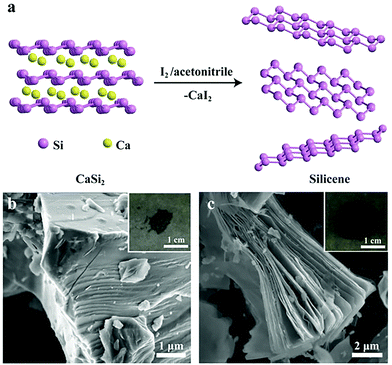 | ||
| Fig. 29 (a) A schematic illustration of the synthesis of silicene from CaSi2via liquid oxidation and exfoliation. SEM images of pristine bulk CaSi2 (b) and the as-reacted product (c), with insets showing photographs. Reprinted with permission from ref. 366. Copyright: ©2018, WILEY-VCH Verlag GmbH & Co. KGaA, Weinheim. | ||
Like other 2D materials, MXenes exhibit crystal geometry with a hexagonal close-packed structure based on the equivalent MAX-phase precursor, and the close-packed structure is formed from M atoms with X atoms occupying octahedral sites.371 According to the formula, there are three representative structures of MXenes: M2XTx, M3X2Tx, and M4X3Tx. In these combinations, X atoms are formed with n layers, whereas M atoms have n + 1 layers (Fig. 30).372 Apart from graphene, MXenes are considered the most dynamic developing material, and they have incredible innovation potential amongst typical 2D nanomaterials because of their remarkable properties, such as hydrophilicity, conductivity, considerable adsorption abilities, and catalytic activity. These vital properties of MXenes suggest their use for various potential applications, including in the photocatalysis, electrocatalysis,373,374 energy,375 membrane-based separation,376,377 and biological therapy378 fields. In this section, we focus on describing new developments relating to MXenes that are utilized for electrocatalytic and energy storage applications, competing as alternatives to graphene materials.
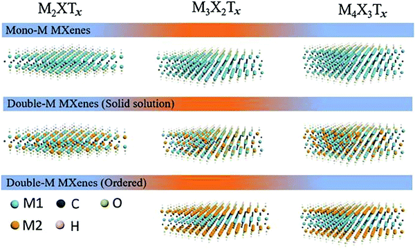 | ||
| Fig. 30 The structures of MXenes with different formulas (M2XTx, M3X2Tx, and M4X3Tx) and their compositions (mono-M MXenes and double-M MXenes). Reprinted with permission from ref. 372. Copyright: ©2019, WILEY-VCH Verlag GmbH & Co. KGaA, Weinheim. | ||
Interestingly, due to the presence of abundant terminal groups, mainly –O, –OH, and –F, and their modifying nature, MXenes can exhibit outstanding hydrophilic properties and high conductivity and charge carrier mobility, making them a very attractive material for various electrocatalytic applications, such as the hydrogen evolution reaction, oxygen evolution reaction, oxygen reduction reaction, nitrogen reduction reaction, and CO2 reduction reaction. To further increase their electrocatalytic activities, recent works involving MXenes have included incorporation with CNTs,379 g-C3N4,380 FeNi-LDH,381 NiFeCo-LDH,382 and metal–organic frameworks.383
Cho and co-workers designed and developed MXene–TiO2 2D nanosheets via the surface oxidation of MXene with defect-free control. These MXene–TiO2 2D nanosheets were successfully implemented in nano-floating-gate transistor memory (NFGTM) providing a floating gate (i.e., multilayer MXene) and tunneling dielectric (i.e., the TiO2 layer). A process of oxidation in water further represented a cost-effective and environmentally benign method, as depicted in Fig. 31. The MXene NFGTM with an optimal oxidation process displayed exceptional nonvolatile memory features, having a great memory window, high programming/erasing current ratio, long term retention, and high durability.384
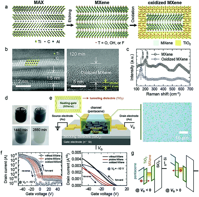 | ||
| Fig. 31 (a) A schematic diagram of the synthesis of 2D Ti3C2Tx MXene and its controlled oxidation. (b) Cross-sectional STEM images of pristine MXene and oxidized MXene. (c) Raman spectra of pristine MXene and oxidized MXene. (d) Photographic images of MXene solution at different stages of oxidation. (e) A schematic illustration of MXene NFGTM. The right panel shows an optical microscopy (OM) image of the oxidized MXene on the SiO2 blocking dielectric layer. (f) The transfer characteristics of transistors with different hysteresis behavior. (g) A schematic diagram of the energy bands of MXene NFGTM corresponding to hole trapping and detrapping in the MXene floating gate. Reprinted with permission from ref. 384. Copyright: ©2020, WILEY-VCH Verlag GmbH & Co. KGaA, Weinheim. | ||
There have been some exciting reports on 2D materials from the pnictogen family, particularly phosphorene. Recently, more attention has also been given to the remaining group 15 elements,390 with the novel 2D materials arsenene, antimonene, and bismuthene being obtained from the key elements arsenic, antimony, and bismuth, respectively. It is reported that 2D monolayers of group 15 elements, including phosphorene allotropes, have five distinct honeycomb (α, β, γ, δ, and ε) and four distinct non-honeycomb (ζ, η, θ, and ι) structures, as depicted in Fig. 32. Dissimilar crystal orientations were found for single-layered As, Sb, and Bi. Zeng and co-workers also reported comprehensive density functional theory (DFT) computations that proved the energetic stability and broad-range application of these materials in 2D semiconductors.391 Previously, following theoretical predictions, Wu and co-workers successfully demonstrated that α-phosphorene showed lowest energy configurations in both honeycomb and non-honeycomb nanosheets.392 In contrast, Zeng and co-workers proved that the buckled forms of 2D sheets of As, Sb, and Bi allotropes are the most stable structures, particularly their β phases.391
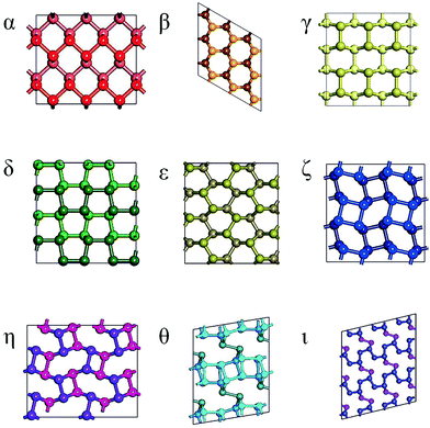 | ||
| Fig. 32 Top views of relaxed group 15 monolayer allotropes with five typical honeycomb structures (α, β, γ, δ, and ε) and four typical non-honeycomb structures (ζ, η, θ, and ι). Reprinted with permission from ref. 391. Copyright ©2016, WILEY-VCH Verlag GmbH & Co. KGaA, Weinheim. | ||
Among monolayer group 15 family materials, 2D sheets of arsenic (As) and antimony (Sb) have gained considerable attention from researchers.393,394 Studies have shown that As and Sb exhibit better stability than black phosphorus; they are highly stable at room temperature and less reactive to air, likely inhibiting the oxidization process.395–398 Nevertheless, it has been demonstrated that the oxidation process is perhaps favorable for fine-tuning the electronic properties; increases in the indirect band gaps ranging from 0 to a maximum of 2.49 eV are found in free-standing arsenene and antimonene semiconductors.399–403 Simultaneously, arsenene and antimonene can also be transformed into semiconductors with direct band gaps. These two 2D nanosheets can be used to design mechanical sensors, moving beyond common electronic and optoelectronic applications. These two extraordinary 2D nanosheets have been studied for their structural–property relationships via first-principles methods.403–405
Continuing the characterization and structural property studies of arsenene carried out by Kamal404et al. and Zhang403et al., Anurag Srivastava and co-workers analyzed applications of arsenene to explore the possibility of improving sensor devices that can be utilized to detect ammonia (NH3) and nitrogen dioxide (NO2) molecules.406,407 They investigated the affinities of NH3 and NO2 molecules for pristine arsenene sheets, examining the binding energies, bonding distances, density distributions, and current–voltage features. The results showed that arsenene 2D sheets are highly durable, with significant electronic charge transfer. They also considered germanium-doped arsenene and characterized the 2D lattice based on molecular affinity relationships with respect to the dopant.
However, the incorporation of any dopants into 2D nanomaterials not only results in experimental difficulty but it also lowers the stability of 2D materials.408 Recently, Dameng Liu and co-workers reported the electronic structures, focusing on band structures, band offsets, and intrinsic defect properties, of few-layer arsenic and antimony.409 The spontaneous oxide passivation layer that is formed naturally on pristine antimonene provides excellent stability.410 Very recently, Stefan Wolff and co-workers conducted DFT calculations on various single or few-layer antimony oxide structures to describe the stoichiometry and bonding type. Interestingly, the samples exhibited various structural stabilities and electronic properties with a wide range of direct and indirect band gaps. Showing band gaps between 2.0 and 4.9 eV, these 2D layers of antimonene exhibited the potential to be used as insulators or semiconductors.411 The same group also analyzed Raman spectra and discussed identifying the predicted antimonene oxide structures experimentally. The enduring task of exploring the utility of antimonene has boosted recent research interest in 2D nanomaterials due to the broad range of potential applications, such as their use in electrochemical sensors,412,413 stable organic solar cells,414 and supercapacitors415 to name a few.
5.3.4.1. Electrochemical applications. The tunable structures and tailorable features of 2D-MOFs have allowed high performance for many electrochemical applications. Most importantly, the featured high specific surface areas of 2D-MOFs have gained much attention for use in supercapacitors. For example, a recent work by Zheng and co-workers proved that cobalt-based 2D-MOFs synthesized using polyvinylpyrrolidone as a surfactant under mild solvothermal conditions could show higher specific capacitance due to the large surrounding area (Fig. 33). The developed 2D Co-MOF nanosheets have shown a maximum specific capacitance of 1159 F g−1 at a current density of 0.5 A g−1.425 Similarly, Wang and his colleagues developed ultrathin nanosheets from NiCo-MOFs with thicknesses ranging from 1.74–3.87 nm and these were compared with pristine Ni-MOFs and Co-MOFs obtained following the same synthetic protocol. The obtained cyclic voltammetry curves revealed that the NiCo-MOF-nanosheet-based electrode yielded a larger CV area than the Ni-MOF and Co-MOF electrodes.426
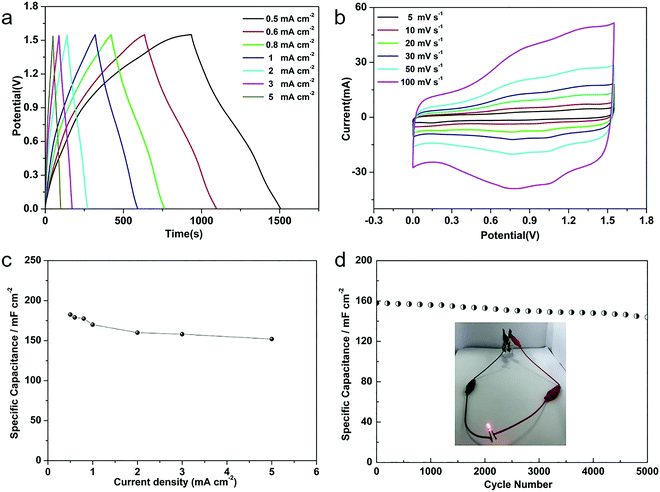 | ||
| Fig. 33 Electrochemical studies of an as-prepared ultrathin 2D Co-MOF NS//activated carbon aqueous device. (a) The galvanostatic charge–discharge curves at different current densities. (b) The cyclic voltammetry curves at different scan rates. (c) Specific capacitances at different current densities. (d) Charge–discharge cycle testing at a current density of 0.5 A cm−2 in 3.0 M KOH electrolyte (inset: a red LED powered by the aqueous device). Reprinted with permission from ref. 425. Copyright: ©2019, Elsevier B.V. All rights reserved. | ||
The 2D MOF nanosheets are also evaluated for the development of high-performance power-storage devices. For example, Li et al.427 recently reported two novel Mn-2D MOFs and Ni-2D MOFs as anode materials for rechargeable lithium batteries. The Mn-based ultrathin metal–organic-framework nanosheets, due to thinner nanosheets, a higher specific surface area, and smaller metal ion radius, had structural advantages over Ni-based ultrathin metal–organic-framework nanosheets. Due to these features, the Mn-based ultrathin metal–organic-framework nanosheets displayed a high reversible capacity of 1187 mA h g−1 at 100 mA g−1 for 100 cycles and a rate capability of 701 mA h g−1 even at 2 A g−1.
The expensive metal oxides utilized in the catalytic process can be replaced in due course by 2D-MOF-based nanosheets with exposed metal sites that impart an adjustable pore structure, ultrathin thickness, a high surface-to-volume atom ratio, and high design flexibility. As a result, 2D-MOFs have extensively been explored for various electrocatalytic applications, including the hydrogen evolution reaction (HER), oxygen evolution reaction (OER), oxygen reduction reaction (ORR), and carbon dioxide reduction reaction (CO2RR). For example, Marinescu et al.428 combined cobalt dithiolene species with benzenehexathiol (BHT) and yielded 2D-MOFs capable of acting as electrocatalysts for the HER in water (Fig. 34). In the presence of 2D-MOF sheets, a high current density of 41 mA cm−2, at −0.8 V vs. SHE and a pH value of 1.3, is observed. Similarly, Feng et al.429 also developed single-layer Ni-based 2D-MOF sheets that are highly effective for electrocatalytic hydrogen evolution. Later, Patra et al.430 reported similar 2D sheets from covalent organic frameworks (2D-COFs) as metal-free catalysts for HER applications. 2D-MOFs are also being explored as active catalysts for the OER process. For example, Xu et al.431 reported the preparation of 2D Co-MOF sheets using polyvinylpyrrolidone as a surfactant under mild solvothermal conditions. These novel 2D Co-MOFs displayed ultrathin nanosheets with many surface-based metal active sites, improving the overall OER performance.
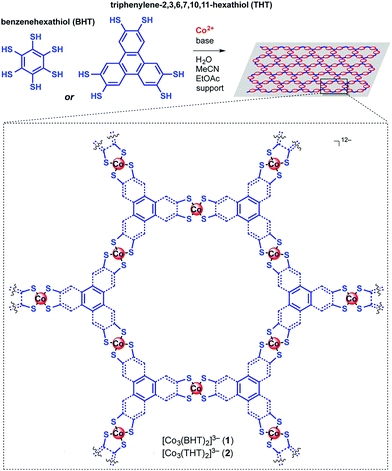 | ||
| Fig. 34 The synthesis of the cobalt dithiolene films 1 and 2 through a liquid–liquid interfacial reaction. The synthesized films are deposited onto desired supports, generating MOS 1 and 2. Reprinted with permission from ref. 428. Copyright: ©2015, American Chemical Society. | ||
Interestingly, experimental electrochemical measurement data showed that Co-MOF sheets offer a low overpotential (i.e., 263 mV at 10 mA cm−2). Similarly, Wang et al.432 also reported that double-metal 2D-sheets (2D NiFe MOFs) consisting of a very ultrathin structure with a thickness of ∼10 nm further offer a low overpotential of 260 mV at 10 mA cm−2. In other reports, Zhang et al.433 successfully performed the OER process with ultrathin 2D-MOF sheets prepared via electrochemical and chemical exfoliation strategies.
Recent work on the catalytic activity of 2D-MOFs has also been reported in relation to the ORR and CO2RR because of their layered crystal structures and high-volume modifiable porous structures. For example, Dincă et al.434 demonstrated that ultrathin layered conductive sheets of the 2D-MOF Ni3(HITP)2 (HITP = 2,3,6,7,10,11-hexaiminotriphenylene) could actively be utilized as a catalyst in an alkaline medium for the ORR process. These 2D-MOF sheets show high stability while retaining 88% of the initial current density over 8 h at 0.77 V vs. RHE. In another report, through fabricating CoxZn2−x(bim)4 2D-sheets as precursors, Zhao et al.435 successfully synthesized cobalt nanodots (Co-NDs) with bimetallic CoxZn2−x(bim)4 nanosheets encapsulating few-layer graphene (Co@FLG). For the CO2RR, a cobalt–porphyrin-containing 2D-MOF was achieved for the selective electrochemical reduction of CO2 to CO with enhanced stability by Peidong Yang and co-workers.436 The results further proved that these thin-film catalysts have the highest selectivity for CO (i.e., 76%) at −0.7 V vs. RHE with the little-to-no substantial decrease in activity over 7 h at −0.7 V vs. RHE, and 16 mL of CO was produced. Besides, like many other porous materials, 2D-MOFs were also shown to be a supporting platform for catalytic nanoparticles because of their high specific surface areas and favorable porosity distributions. To this end, an example can be noted from Wang et al.437 reporting that fine porous MOF-5 nanosheets can be utilized to immobilize Pd nanoparticles.
5.3.4.2. Sensing platforms. Considering the growing demand for high-performance sensors, the development of practical nanomaterials, particularly 2D-MOFs, has attracted great importance in the fluorescence sensing field to detect small gas molecules, metal ions, organic solvents, and biomolecules.438–440 Taking account of their unique physical and chemical properties together with their structural integrity, 2D-MOFs offer auspicious possibilities for sensing applications. So far, 2D-MOFs have been used in the optical and electrochemical sensing platforms and they have been applied to the sensing of DNA,441–443 microRNA,419 and adenosine.418,444 In biosensing applications, for example, Zhang et al.441 reported a simple surfactant-assisted synthetic route for developing ultrathin 2D-MOF sequences with various metals (M-TCPP: M = Zn, Cu, Cd, or Co; TCPP = tetrakis(4-carboxyphenyl)porphyrin) and a sensor that could be effectively employed in the detection of DNA (Fig. 35). The experimental results show that the copper analogue 2D Cu–TCPP nanosheets performed best at sensing DNA out of four different metals. This counterpart exhibited a detection limit of 20 × 10−12 M, and this detection limit is substantially lower than previously reported MOF-based fluorescence assays. The fluorescence quenching nature was later studied for two-color intracellular adenosine imaging in living cells by Xia et al.418 Besides being used as quenchers, 2D-MOFs can also be a part of fluorescence-based emitters; fluorescein isothiocyanate (FITC) was covalently conjugated to UiO MOFs and this system exhibited excellent ratiometric pH-sensing and enhanced fluorescence properties, as reported by Lin and co-workers.445
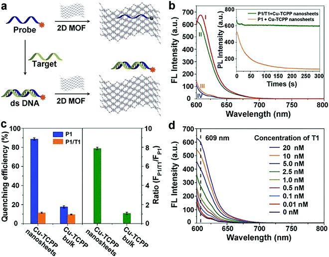 | ||
| Fig. 35 DNA detection with 2D MOFs (Cu–TCPP, Zn-TCPP(Fe), and Co-TCPP). (a) A schematic illustration of the 2D-MOF-nanosheet-based fluorescence assay for DNA. (b) Fluorescence spectra under different experimental conditions: (I) P1; (II) P1 + T1 + Cu–TCPP nanosheets; (III) P1 + Cu–TCPP nanosheets; and (IV) Cu–TCPP nanosheets. The concentrations of P1, T1, and Cu–TCPP nanosheets in the final solutions are 2.5 × 10⁻⁹ M, 20 × 10−9 M, and 35 μg mL−1, respectively. Inset: A kinetics study of the fluorescence changes of the P1 and P1/T1 duplexes in the presence of Cu–TCPP nanosheets; the excitation and emission wavelengths are 588 and 609 nm, respectively. (c) Left: The quenching efficiency (η) of Cu–TCPP nanosheets and bulk Cu–TCPP MOFs for P1 and P1/T1; right: the fluorescence intensity ratio (FP1/T1/FP1) values at 609 nm in the presence of Cu–TCPP nanosheets (35 μg mL−1) or bulk Cu–TCPP MOFs (35 μg mL−1). FP1/T1 is the fluorescence intensity of dsDNA (P1/T1) at 609 nm in the presence of Cu–TCPP nanosheets or bulk Cu–TCPP MOFs. FP1 is the fluorescence intensity of ssDNA (P1) at 609 nm in the presence of Cu–TCPP nanosheets or bulk Cu–TCPP MOFs. The concentrations of P1 and T1 in the final solution are 2.5 × 10⁻⁹ and 20 × 10−9 M. (d) Fluorescence spectra of P1 (2.5 × 10⁻⁹ M) in the presence of T1 at different concentrations in 2D Cu–TCPP nanosheet solution (35 μg mL−1). Reprinted with permission from ref. 441. Copyright: ©2015, WILEY-VCH Verlag GmbH & Co. KGaA, Weinheim. | ||
5.3.4.3. Membrane-based gas separation. In membrane-based gas separation, the key parameters that characterize the membrane process are permeability (how productive the separation process is) and selectivity (how efficient the separation process is). Due to the nanometer thickness and controlled pore structure distribution, 2D-MOFs have been recognized as a new type of membrane material amongst other gas-separation membranes. To better understand the performance of 2D MOF nanosheets, Yang et al.446 examined the potential applicability of 2D-MOFs via employing ultrathin molecular sieving membranes for H2/CO2 separation. A layered poly[Zn2(benzimidazole)4] MOF, denoted as Zn2(bim)4, with a sheet thickness approximately less than 1 nm, crystalline nature, and high lateral area was synthesized. This monolayered Zn2(bim)4 nanosheet colloid, when dropped on porous ceramic (α-Al2O3) substrates at high temperature, resulted in a defect-free membrane with several-nanometer thickness. The resultant membrane displayed excellent H2 gas molecule separation abilities, with permeance varying from 760 to a maximum of 3760 GPU together with the variation of H2/CO2 selectivity from 53 to a maximum of 291. Later reports from the same group showed H2 permeance of up to 8 × 10⁻⁷ mol m−2 s−1 Pa−1 with a H2/CO2 separation factor of 166 upon developing another 2D-MOF membrane from Zn2(bim)3(OH) nanosheets.447 Recently, Zhu et al.448 reported a novel defect-free membrane from the 2D-MOF Ni3(HITP)2 (HITP = 2,3,6,7,10,11-hexaaminotriphenylene) via a filtration-based fabrication method on ordered macroporous anodized aluminum oxide (AAO) (Fig. 36). The corresponding membranes exhibited high mechanical stability, long-lasting characteristics, and good reproducibility, making them potential candidates for practical applications such as enhanced gas separation. Furthermore, gas-separation measurements revealed that the Ni3(HITP)2 membrane could obtain high CO2 gas permeance together with enhanced selectivity over other light gases, particularly N2. The CO2 permeance of the Ni3(HITP)2 membrane was 3.15 × 10⁻⁶ mol m−2 s−1 Pa−1 with pure gas separation factors of 13.6 and 7.8 for CO2/N2 and H2/N2 gas pairs, respectively. Apart from pure 2D-MOF-nanosheet-containing membranes, the utilization of 2D-MOFs in mixed-matrix membranes (MMMs) was also reported via the simple blending of 2D-MOFs into a polymer matrix for enhanced gas-separation applications.449–452
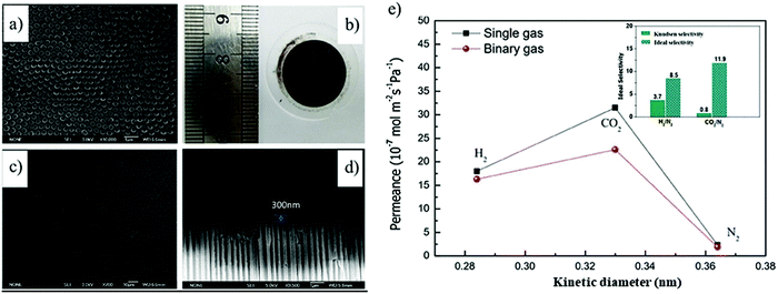 | ||
| Fig. 36 (a) An SEM image of a bare porous AAO support; (b) an image of MOF membranes obtained via filtration; and (c) an SEM top view and (d) cross-sectional view of the Ni3(HITP)2 membrane on an AAO support. (e) Single and binary gas permeance levels through a Ni3(HITP)2 membrane measured at 298 K and 1.2 bar (inset: the separation factors from equimolar mixed gas permeation tests). Reprinted with permission from ref. 448. Copyright: ©2020, Wiley-VCH Verlag GmbH & Co. KGaA, Weinheim. | ||
5.3.4.4. Other applications. Apart from the above-mentioned wide-ranging applications of 2D-MOFs, their effectiveness has been broadened even further because of ever-increasing interest in nanomaterials due to their distinctive physical and chemical properties. The practical applicability of 2D-MOFs has been demonstrated in many other fields, such as matrix-assisted laser desorption ionization (MALDI),453 gas adsorption,454–456 and chiral separation.457 For example, Zhi-Yuan Gu and co-workers developed a 2D-MOF from Zn2(bim)4 nanosheets, which is stable in water and overcame known matrix difficulties by means of exhibiting an exceptional surface area, efficient photon absorption, and high ionization efficiency.453 The newly synthesized 2D MOF Zn2(bim)4 nanosheets showed a layered stable structure, a large accessible surface area, a strong Tyndall effect, and homogeneity as a matrix suspension. Results proved that 2D MOF Zn2(bim)4 nanosheets can be applied in the analysis of amino acids and hormones as a MALDI-TOF MS matrix. Tang et al.457 developed chiral 2D-MOFs for chiral-related separation applications, which are unprecedented in the 2D-MOF family. They used an inverse microemulsion method to prepare chiral L(D)-Thr-Zn nanosheets via reacting chiral N-(4-pyridylmethyl)-L(D)-threonine ligands with Zn(CH3COO)2. Due to the presence of a high number of exposed chiral sites on the surface of the newly developed ultrathin chiral L(D)-Thr-Zn nanosheets, extraordinary enantioselectivity during the chiral separation of the racemic Cr(oxalate)33− complex and atomically precise [Ag28Cu12(SR)24]4− (SR = 2,4-dichlorobenzenethiol) nanoclusters are achieved.
5.4. Metal-based nanostructured materials
Metal-based nanomaterials are continuously being investigated for a wide range of applications due to their promising features.458,459 The design of nanoscale catalysts has emerged as a significant research area due to their exceptionally high catalytic activities allowing reactions to be achieved more effectively and efficiently. Materials at the nanoscale level provide rich surface textural features, enormous numbers of binding sites, large surface areas, and extremely small sizes, favoring the thermodynamics and kinetics of transportation for heterogeneous reactions.460 Metal-based nanostructured materials are also being explored for the production of next-generation artificial enzymes.461 More focus has been directed toward designing specific nano-architectures to achieve better performance from these metal-based materials. A range of methods is available for the synthesis of metal-based nanostructured materials. Metal-based nanostructured materials can be synthesized via hydrothermal, solvothermal, sol–gel, electroless, electrochemical, and physical methods.66As discussed, catalysis is one of the main uses of metal-based nanostructured materials. A continuous increase in the demand for energy, the rapid depletion of conventional energy reservoirs, and rising concerns over the emission of CO2 have increased the challenges and urgency in the energy field.460 Metal-based nanostructured materials are extensively being explored to produce alternative clean and renewable energy sources. A range of metal-based nanomaterials has been evaluated and is under consideration for developing robust electrodes that can be effectively applied to water splitting, batteries, and solar cells.
High energy demands have led to more pressure to improve the performances of existing highly demanded lithium-ion batteries. Researchers have focused on improving their lifetimes, sizes, and safety.462 Nanostructured metal-oxide-based materials are promising electrode materials for use in high-performance charge-storage devices. A metal-based nanostructured electrode is evaluated as both the anode and cathode to overcome the challenges of conventional electrodes.463 In a conventional LIB, LiCoO2 was used as the cathode material. Controlled morphology plays a crucial role in determining the performance of a material. Powder composed of spherical particles of LiNi0.8Co0.2O2 showed a higher tap density compared to irregular particles and the material substantially improved the power density of secondary lithium batteries.464 Hierarchical nanostructures of metal-based oxides (such as 3D hierarchical ZnCo2O4 nanostructures) have emerged as a new trend for the development of high-capacity electrodes for lithium-ion batteries.465 Since their commercialization by Sony in the early 1990s, LIBs have achieved tremendous success in bringing portable electronic devices to the market. However, their sustainable development on the grid-scale is hampered due to limited Li resources in nature, and this is causing a continuous increase in cost.466 Sodium-ion batteries are in the spotlight to replace powerful lithium-ion batteries due to the widespread availability of sodium and its lower cost compared with lithium.467 It is essential to note that, in terms of energy densities for SIBs, it is difficult to bypass LIBs because of the low standard electrochemical potential and higher weight of Na. SIBs could be proved to be ideal for those applications where cost is a critical factor compared to energy density.466
SIBs also operate similarly to LIBs, based on an intercalation mechanism. SIBs also consist of cathode and anode electrodes separated through an electrolyte. During the charging process, sodium ions are extracted from the cathode and inserted into the anode via the electrolyte. In the discharging process, the electrons leave the anode through an external circuit to reach the cathode, providing electricity to the load, whereas Na+ moves to the cathode during this process. The radius of Na+ (1.02 Å) is greater than that of Li+ (0.76 Å), making it challenging to intercalate into electrode materials.468 Thus, appropriate electrode materials are required in which fast Na-ion insertion and extraction is possible. However, SIBs are suffering from a lack of appropriate electrode materials. It is important to develop electrode materials that have enough interstitial space within their crystallographic structures and better electrochemical performance. Among the various proposed electrode materials, NaxMO2 layered transition-metal oxides (M = V, Fe, Cu, Co, Ni, Cr, Mn, and their combinations) are considered to be promising electrode materials for SIBs. Layered metal oxides are considered to be promising electrode materials due to their facile scalable synthesis, simple structures, appropriate operating potentials, and high capacities.469,470 Large volume expansion and poor kinetics during the charge–discharge process can severely affect the cyclability and performance of SIBs. One of the effective strategies to deal with the mechanical stress triggered by large volume changes is the design of hollow or porous structures. In response, three-dimensional network-based Sb2O3@Sb composite anode materials can help to relieve the volume-change-related stress through their uniform porous networks and provide better transportation channels for Na+.471
The large volume expansion of electrodes can also be buffered via designing 2D metal-oxide materials with large interlayer spacing. The ultrathin nanosheets provide high reversible capacity with enhanced cycling stability and contribute to providing reaction sites for electrons/ions, decreasing the diffusion distance, providing effective diffusion channels, and facilitating fast charge/discharge for sodium and lithium. 2D SnO nanosheet anodes were evaluated for SIBs. The capacity and cyclic stability improved, as the number of atomic SnO layers is decreased in the sheets.472 Sb is a promising anode material, but during the sodiation/desodiation processes, huge volume expansion of 390% is observed, which hinders its practical use. Nanostructured Sb in the form of nanorod arrays with large interval spacing displays the great capacity to accommodate volume changes during cycling.473 A comparison of various nanostructured metal-based electrodes for various charge storage purposes is shown in Table 3. Overall, well-structured metal or metal-based oxide nanomaterials have the capacity to resolve current issues relating to charge storage devices.
| Nanostructured metal oxide | Synthesis route | Charge storage device | Rate capabilities | Retention capacity and cyclability | Ref. |
|---|---|---|---|---|---|
| Mesoporous NiCo2O4 nanowire arrays | A surfactant-assisted hydrothermal method and short post-annealing treatment | LIB, SC | ≈1012 mA h g−1 at 0.5 A g−1, 1010 F g−1 at 20 A g−1 | Retained 854 mA h g−1 after 100 cycles, negligible specific capacitance decay after 5000 cycles at 8 A g−1 | 474 |
| Zn0.25V2O5·nH2O nanobelts | A microwave hydrothermal method | ZIB | ∼300 mA h g−1 at 50 mA g−1 | Capacity retention of 80% at 10C after 1000 cycles | 475 |
| Leaf-like CuO nanostructures | In situ precipitation-induced growth and thermal annealing | LIB | 549 mA h g−1 at 0.1 A g−1 | 95.5% after 200 cycles | 476 |
| 3D porous copper skeleton supported zinc anode | Electrodeposition | ZIB | 364 mA h g−1 at 0.1 A g−1 | Retained a capacity of 173 mA h g−1 at 0.4 A g−1 after 300 cycles | 477 |
| ZnO–carbon black nanostructured anode materials | An atomic layer deposition method | LIB | 2096 mA h g−1 at 100 mA g−1 | A specific capacity of 1026 mA h g−1 was maintained after 500 cycles | 478 |
| NiCo2O4 nanoneedle array | A hydrothermal method combined with post-heat treatment | SIB | 400 mA h g−1 at 50 mA g−1 | ∼215 mA h g−1 after 50 cycles | 479 |
| Coral-like nanostructured Sb2O3@Sb anode | Heating in a furnace | SIB | 497.3 mA h g−1 at 3000 mA g−1, 724.3 mA h g−1 at 1000 mA g−1 | 574.8 mA h g−1 at 100 mA g−1 after 150 cycles | 471 |
| 3D Fe2GeO4/N-CNSs | A high-temperature calcination process | SIB | 350 mA h g−1 at 0.1 A g−1, 180 mA h g−1 at 22.8 A g−1 | ∼86% reversible capacity retention after 6000 cycles | 480 |
| MnO2 nanoflowers | A hydrothermal method and thermal treatment | SIB | 487.8 mA h g−1 at 50 mA g−1 | 103.3 mA h g−1 at 800 mA g−1 after 100 cycles, 133.6 mA h g−1 at 400 mA g−1 after 1000 cycles | 481 |
| 2D SnO nanosheet anodes | A hydrothermal method | SIB | 1072 mA h g−1 at 0.1 A g−1 (discharge), 848 mA h g−1 at 0.1 A g−1 (charge) | 665 mA h g−1 at 0.1 A g−1 after 100 cycles, 452 mA h g−1 at 1.0 A g−1 after 1000 cycles | 472 |
| TiO2/C nanofibers | Electrospinning | SIB | 164.9 mA h g−1 at 2000 mA g−1 | Nearly 100% capacity retention over 1000 cycles | 482 |
| Sb nanorod arrays | A template method | SIB | 557.7 mA h g−1 at 20 A g−1 | 84% at 0.2 A g−1 over 250 cycles | 473 |
| CuCo2O4-nanodot-inserted N-doped carbon nanofibers | Electrospinning | SIB | 296 mA h g−1 at 5000 mA g−1 | 314 mA h g−1 at 1000 mA g−1 after 1000 cycles | 483 |
Recently, an immense focus of research has been to produce H2 fuel via water-splitting to replace conventional fossil fuels. This will help to eliminate emissions from the use of carbonaceous species.484 Electrochemical method are considered simple water splitting approaches, as these methods only require an applied voltage and water as inputs to produce hydrogen fuel.485 The coupling of solar irradiation to electrochemical water splitting has enhanced the performance and reduced the process cost. Due to these reasons, this has become a hot area of research.486 During water electrolysis, H2 is produced through the hydrogen evolution reaction at the cathode and O2 is produced through the oxygen evolution reaction at the anode. However, water splitting is not so straightforward, and it requires an efficient catalyst that can facilitate the splitting of water. Metal- and metal-oxide-based catalysts are extensively being explored for water splitting. For the HER reaction, Pt-based catalysts are found to be suitable, whereas for OER reactions, Ir-/Ru-based compounds are found to be benchmark catalysts. Scarcity and high cost have limited the widespread use of these metals. The barrier of noble-metal cost can be mitigated through developing noble-metal nanostructured surfaces that produce more active sites or via depositing monolayers of noble metals on low-cost materials. The alloying of noble metals with other metals has enhanced site-specific activity.484 At present, more focus is being placed on developing noble-metal-free catalysts for water splitting.485 Usually, an efficient electrocatalyst is characterized by:487 a low overpotential; high stability; low production costs; and high electrocatalytic activity.
The nano-structuring of catalysts is an effective tool to boost their surface areas. The electrolysis of water occurs at the surface of a catalyst, and nanostructured catalysts provide more active sites and the better diffusion of ions and electrolytes.484 Non-noble metals that are under observation for the development of HER electrocatalysts include nickel (Ni), tungsten (W), iron (Fe), molybdenum (Mo), cobalt (Co), and copper (Cu).487 For instance, a noble metal-free catalyst, carbon-decorated Co3O4 nanoarrays on carbon paper, required a small overpotential of 370 mV to reach a current density of 10 mA cm−2. It can maintain a current density of 100 mA cm−2 for 413.8 h and 86.8 h under alkaline and acidic conditions, respectively.488
Metal-based semiconductor materials play a crucial role in a range of applications. For photoelectrochemical water splitting, the semiconductor material plays a central role in the solar-to-hydrogen conversion efficiency. Some critical features are prerequisites when it comes to selecting the right semiconductor material for the photoelectrochemical splitting of water:489 an extraordinary capacity to absorb visible light; an appropriate bandgap; suitable valence and conduction band positions; commercial feasibility; and chemical stability.
For an ideal semiconductor for water splitting, the valence band and conduction band edge positions must straddle the oxidation and the reduction potentials of water. Metal oxides have received significant attention among semiconductors due to their wide band gap distributions, remarkable photo-electrochemical stabilities, and favorable band edge positions.490 Semiconductor-based photoelectrodes become excited upon light irradiation, and electrons from the valence band move to the unoccupied conduction band. Some of the generated electrons at the cathode surface reduce protons to hydrogen gas, whereas holes at the photoanode produce oxygen gas via water splitting.490 As a result, various nanostructured metal oxides can be used as photoelectrode materials, such as WO3,491 Cu2O,492 TiO2,493 ZnO,494 SnO2,495 BiVO4,496 and α-Fe2O3,490 for the efficient splitting of water. As discussed, the nano-structuring of semiconductors can significantly impact the electrode photoelectrochemical performance during water splitting.
Metal-based nanomaterials have been used for the development of sensitive sensors. These metal-based sensors can replace the complex and expensive instruments that are conventionally used for the sensing of analytes. Metal-oxide-based sensors have the interesting characteristics of low detection limits, low cost, high sensitivity, and facile operation.497 Mostly, semiconducting metal-oxide-based sensors are used for the sensing of toxic, flammable, and exhaust gases. Semiconductor metal oxides with a size in the range of 1–100 nm have been significantly investigated as gas sensors due to their size-dependent properties. The geometry and size of a nanomaterial can considerably affect the hole and electron movement in semiconductors.498 The surface-to-volume ratio and surface area are substantially enhanced at the nanoscale level, and this is amazingly beneficial for sensing. Chemiresistive semiconducting metal oxides are potential candidates for gas sensing due to the following features:499 rapid response times; fast recovery times; low cost; simple electronic interfaces; user-friendliness and low maintenance; and abilities to sense a wide range of gases.
Electrode materials decorated with metal- or metal-oxide-based nanostructured materials have shown better responses and selectivity for determining various analytes over conventional electrode materials. The nano-sized metal structures act as an electrocatalyst and electronic wires to provide rapid electron transfer between the transducers and analyte molecules.500 The electrochemical redox reaction of H2O2 can be improved via the thermally controlled anchoring of Pt NPs on the electrode surface.501
Currently, researchers are not just concentrating on the development of randomly shaped nanomaterials; instead, they are very focused on and interested in the rational design of materials with controlled nano-architectures for boosting their performances for specific applications. As a result, extensive research has been carried out to develop metal-based materials with controlled dimensions to achieve better catalytic responses. Particle morphology is a crucial factor in the performance of nanomaterials for specific applications. Laifa Shen et al. rationally designed an electrode architecture via growing mesoporous NiCo2O4 nanowire arrays on carbon textiles, which boosted the electrode performance (Fig. 37).474
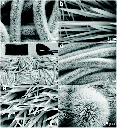 | ||
| Fig. 37 (a) Low- and (b) high-magnification SEM images of a NiCo-precursor NWA/carbon textile composite, showing the nanowires completely surrounding the carbon microfiber core. (c and d) Low- and (e) high-magnification SEM images of a crystalline NiCo2O4 NWA/carbon textile composite. (f) An SEM image of the urchin-like NiCo2O4 microsphere prepared in the absence of carbon textiles. Reprinted with permission from ref. 474. Copyright: ©2013, WILEY-VCH Verlag GmbH & Co. KGaA, Weinheim. | ||
The same materials with different morphologies can produce different outcomes. For instance, MnO2 nanoflowers have provided high initial sodium-ion storage capacity compared with MnO2 nanorods.481 Radha Narayanan and Mostafa A. El-Sayed have analyzed various nanoscale morphologies of Pt, such as tetrahedral, cubic, and near-spherical nanoparticles. The highest rate constant is observed with tetrahedral nanoparticles and the lowest rate constant was observed with cubic nanoparticles, whereas spherical nanoparticles exhibited an intermediate rate constant during catalysis.502 Xiaowei Xie et al. found that Co3O4 nanorods show high activity compared to conventional Co3O4 nanoparticles for the low-temperature oxidation of CO.503 The catalytic activity of metal-based nanomaterials is strongly affected by their shape.504 Shape-defined mesoporous materials (TiO2) have shown superior photoanode activities (Fig. 38).505 As a result, in the literature, several nanostructured morphologies of metal-based materials, such as nanotubes,506,507 nanorods,508,509 nanoflowers,510 nanosheets,511 nanowires,512 nanocubes,513 nanospheres,514,515 nanocages,516 and nanoboxes,517 have been reported for a range of applications.
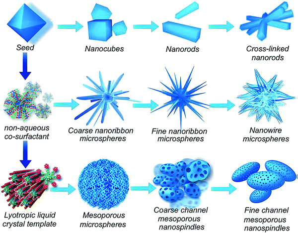 | ||
| Fig. 38 A schematic illustration of the controlled chemical growth of TiO2 nanostructures with desired morphologies. (top row) Path I: the direct growth of nanocubes, rectangular nanorods, and cross-linked nanorods synthesized from seeds in aqueous solutions; (middle row) path II: 3D dendritic structures synthesized from solution with the addition of a non-aqueous co-surfactant; and (bottom row) path III: shape-defined mesoporous TiO2 nanostructures synthesized from solutions with lyotropic liquid-crystal templates. Reprinted with permission from ref. 505. Copyright: © 2016, WILEY-VCH Verlag GmbH & Co. KGaA, Weinheim. | ||
Hollow nanostructures have surfaced as an amazing class of nanostructured material, and they have received significant attention from researchers. Hollow nanostructures have the unique features of:518,519 low density; abundant inner void spaces; large surface areas; and the ability to act as nanoscale containers with high loading capacity, nanoreactors, and nanocarriers.
Various metal-based hollow nanostructures, such as hollow SnO2,520 hollow palladium nanocrystals,521 Co–Mn mixed oxide double-shell hollow spheres,521 hollow Cu2O nanocages,522 three-dimensional hollow SnO2@TiO2 spheres,523 hollow ZnO/Co3O4 nano-heterostructure,524 triple-shell hollow α-Fe2O3,525 and hierarchical hollow Mn-doped Ni(OH)2 nanostructures,526 have been developed for various applications. The presence of nanoscale hollow interiors and functional shells imparts them with great potential for gas sensing, catalysis, biomedicine, energy storage, and conversion.519
From this discussion, it can be concluded that metal-based nanostructured materials have great potential compared to their bulk counterparts. The conversion of materials to the nanoscale is not enough to achieve high performance with better selectivity. Now, research is switching from conventional nanomaterials to more advanced and smartly designed nanomaterials. In modern research, nanomaterials are being designed with better-controlled morphologies and regulated features.
5.5. Core–shell nanoparticles
Nanoparticles can be categorized as simple, composite, or core–shell examples based on whether the nanoparticle consists of a single material or multiple materials. Nanoparticles consisting of single materials are generally called simple nanoparticles. Core–shell and composite nanoparticles are nanoparticles that consist of two or more materials. More precisely, core–shell is a term used for nanomaterials that comprise an inner material, making a core, and an outer material, forming a shell around the core material. Core–shell nanoparticles of different combinations can be developed, such as organic/organic, inorganic/organic, inorganic/inorganic, and organic/inorganic combinations. Fig. 39 demonstrates different classes of core–shell nanomaterials.527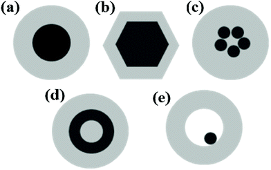 | ||
| Fig. 39 Different core/shell nanoparticles: (a) spherical core/shell nanoparticles; (b) hexagonal core/shell nanoparticles; (c) multiple small core materials coated with a single shell material; (d) a nanomatryushka material; and (e) a movable core within a hollow shell material. Reprinted with permission from ref. 527. Copyright: ©2012, American Chemical Society. | ||
A spherical nanoparticle core–shell nanostructure is a practical way to introduce multiple functionalities on the nanoscopic length scale.528 The properties arising from the core or shell can be different, and these properties can be tuned via controlling the ratio of the constituent materials. The shape, size, and composition play a critical role in tuning the core–shell nanoparticle properties.529 The shell material can help to improve the chemical and thermal stabilities of the core material. The core–shell design has become effective where an inexpensive material cannot be used directly due to its instability or easily oxidizable nature. The core can consist of an easily oxidizable inexpensive metal, whereas the shell might consist of noble metals, oxides, polymers, or silica.530 For instance, magnetic nanoparticles when prepared can be sensitive toward air, acids, and bases. Magnetic nanoparticles can be protected via coating with organic or inorganic shells.528
Core–shell metal nanoparticles are an emerging nanostructured material with great potential in the fields of energy and catalysis.531 The first report of core–shell nanoparticles (2007) for supercapacitor applications consisted of a polyaniline/multi-walled-carbon-nanotube composite (PANI/MWNTs).532 Metal-based core–shell structured nanoparticles have shown enhanced catalytic performance due to their shape-controlled properties.533 Ming-Yu Kuo et al. developed Au@Cu2O core–shell particles with controllable shell thicknesses that acted as a dual-functional catalyst. The shell thickness of Cu2O increased with an increasing concentration of Cu2+ precursor. The thicknesses of the shells of Au@Cu2O-1.5 (12.2 ± 1.7 nm), Au@Cu2O-2 (13.2 ± 1.8 nm), Au@Cu2O-3 (18.2 ± 2.2 nm), and Au@Cu2O-4 (20.8 ± 2.5 nm) due to various concentrations are shown in Fig. 40.534 A NiO@SiO2 core–shell catalyst provided a higher yield of acrylic acid from acetylene hydroxycarbonylation.535 Core–shell architecture can be used to prevent active metal nanoparticles from oxidation during operation. For instance, a plasmonic photocatalyst was developed that consisted of silver nanoparticles embedded in titanium dioxide. The direct contact of Ag with TiO2 could lead to its oxidization; this is prevented via developing core–shell architecture in which Ag is used as the core and SiO2 is used as a shell to protect it.536 Another excellent option is to replace an expensive core with a non-noble metal to reduce the core–shell cost while using a thin layer of a noble metal that consumes a small amount of metal as the shell. This will ensure the prolonged stability of the catalyst during operation.533 Overall, core–shell morphologies provide better catalytic activity due to the synergistic effect of the metallic core–shell components.152
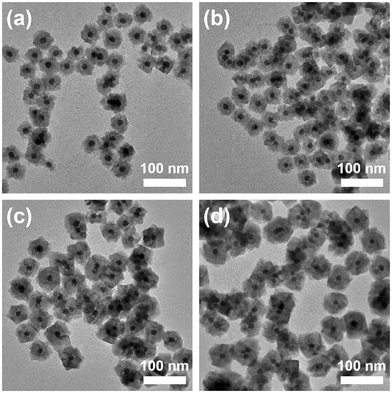 | ||
| Fig. 40 TEM images of (a) Au@Cu2O-1.5, (b) Au@Cu2O-2, (c) Au@Cu2O-3, and (d) Au@Cu2O-4. Reprinted with permission from ref. 534. Copyright: ©2018, Elsevier B.V. All rights reserved. | ||
Among the several classes of nanomaterials, core–shell nanoparticles are found to be more promising for different biomedical applications. For instance, magnetic nanoparticles are considered to be useful for biomedical applications due to the following reasons: (a) aggregation is prevented due to superparamagnetism; (b) delivery and separation can be controlled using an external magnetic field; (c) they can be appropriately dispersed; and (d) there is the possibility of functionalization. A range of magnetic nanoparticles is available, such as NiO, Ni, Co, and Mn3O4. The most famous example is iron oxide, but uncoated iron oxides are unstable under physiological conditions. This may result in controlled drug delivery failure due to improper ligand surface binding and the promotion of the formation of harmful free radicals. Therefore, the formation of shells around magnetic nanoparticles has tremendous significance for biomedical applications.537 One of the approaches is to use gold shells on magnetic nanoparticles. Au NPs are also called surface plasmons and they substantially enhanced the absorption of light in the visible and near-infrared regions. Thus, coating magnetic nanoparticles with a Au shell can result in a core–shell nanostructure that displays both optical and magnetic functionality in combination.529
Numerous biocompatible core–shell nanoparticles are being developed for photothermal therapy, as core–shell materials are found to be useful for photothermal therapy. Hui Wang et al. have developed bifunctional core–shell nanoparticles for dual-modal imaging-guided photothermal therapy. The core–shell nanoparticles consist of a magnetic ∼9.1 nm core of Fe3O4 covered by an approximately 3.4 nm fluorescent carbon shell. The Fe3O4 core leads to superparamagnetic behavior, whereas the carbon shell provides near-infrared (NIR) fluorescence properties. The bifunctional nanoparticles have shown dual-modal imaging capacity both in vivo and in vitro. The iron oxide–carbon core–shell nanoparticles absorbed and converted near-infrared light to heat, facilitating photothermal therapy.538 Au-Based core–shell structures are also being prepared for photothermal therapy. Bulk gold is biocompatible, but Au NPs can accumulate in the spleen and liver, causing severe toxicity. Koo Chul Kwon et al. have developed Au-NP-based core–shell structures that did not result in any gross or histological lesions in the major organs of mice, which revealed that this is a potent and safe agent for photothermal cancer therapy. The core–shell nanoparticles consisted of proteinticle/gold (PGCS-NP) and were developed via proteinticle surface engineering. PGCS-NP was injected intravenously into mice with tumors, and the injected core–shell nanoparticles successfully reached the EGFR-expressing tumor cells. The tumor size was significantly reduced upon exposure to near-infrared laser irradiation (Fig. 41). No accumulation of Au NPs was observed in the mice organs, which indicated that PGCS-NP disassembled into many tiny gold dots, which were easily excreted by the kidneys and liver without causing any toxicity.539 In another example, multifunctional Au@graphene oxide nanocolloid core@shell nanoparticles were developed, in which the core and shell consisted of gold and a graphene oxide nanocolloid, respectively. The developed core–shell structure showed multifunctional properties, allowing Raman bioimaging and photothermal/photodynamic therapy with low toxicity.540 Apart from this, numerous other core–shell nanoparticles, such as polydopamine–mesoporous silica core–shell nanoparticles,541 AuPd@PVP core–shell nanoparticles,542 Au@Cu2−xS core–shell nanoparticles,543 bismuth sulfide@mesoporous silica core–shell nanoparticles,544 and Ag@S-nitrosothiol core–shell nanoparticles, have been used for photothermal therapy.545
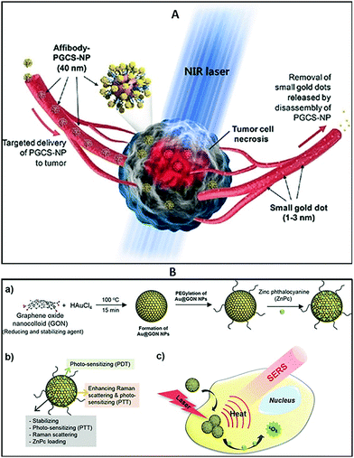 | ||
| Fig. 41 (A) PGCS-NPs (40 nm) for the excellent photothermal therapy of cancer. Reprinted with permission from ref. 539. Copyright: ©2014, WILEY-VCH Verlag GmbH & Co. KGaA, Weinheim. (B) The synthetic procedure (a), multifunctionality (b), and theranosis process (c) of ZnPc–PEG–Au@GON NPs. Reprinted with permission from ref. 540. Copyright: ©2015, WILEY-VCH Verlag GmbH & Co. KGaA, Weinheim. | ||
Due to their unique features and the combination of properties from the shell and core, these core–shell nanoparticles have received considerable interest in many fields, ranging from materials chemistry to the biomedical field. For electrochemical reactions, the core–shell structure conductivity can be enhanced via conducting polymers, carbon materials, and metals. Core–shell nanoparticles as electrode materials showed better performance compared to single components. Most of the core materials are prepared via hydrothermal methods, and shells can be prepared via hydrothermal or electrodeposition methods.546 Even though significant progress has been made relating to the synthesis methods of core–shell materials, a major challenge is the high-quality production of core–shell materials in more effective ways for required applications, specifically biomedical applications.
6. Challenges and future perspectives
Currently, huge numbers of theoretical and experimental literature studies of nanomaterials and nanotechnology have been witnessed. Future technologies depend upon how effectively materials can be manipulated on the nanoscale for various applications. However, at the same time, the development and effective utilization of nanomaterials involve many challenges. Some of the critical challenges are mentioned below:(a) The presence of defects in nanomaterials can affect their performance and their inherent characteristics can be compromised. For instance, carbon nanotubes are one of the strongest materials that are known. However, impurities, discontinuous tube lengths, defects, and random orientations can substantially impair the tensile strength of carbon nanotubes.547
(b) The synthesis of nanomaterials through cost-effective routes is another major challenge. High-quality nanomaterials are generally produced using sophisticated instrumentation and harsh conditions, limiting their large-scale production. This issue is more critical for the synthesis of 2D nanomaterials. Most of the methods that have been adopted for large-scale production are low cost, and these methods generally produce materials with defects that are of poor quality. The controlled synthesis of nanomaterials is still a challenging job. For example, a crucial challenge associated with carbon nanotube synthesis is to achieve chiral selectivity, conductivity, and precisely controlled diameters.548,549 Obtaining structurally pure nanomaterials is the only way to achieve the theoretically calculated characteristics described in the literature. More focused efforts are required to develop new synthesis methods that overcome the challenges associated with conventional methods.
(c) The agglomeration of particles at the nanoscale level is an inherent issue that substantially damages performance in relevant fields. Most nanomaterials start to agglomerate when they encounter each other. The process of agglomeration may be due to physical entanglement, electrostatic interactions, or high surface energy.550 CNTs undergo van der Waals interactions and form bundles, making it difficult to align or properly disperse them in polymer matrices.159 Similarly, graphene agglomeration is triggered by the basal planes of graphene sheets due to π–π interactions and van der Waals forces. Due to severe agglomeration, the high surface areas and other unique graphene features are compromised. These challenges hinder the practical application of high-throughput electrode materials or composite materials for various applications.551
(d) The efficiency of nanomaterials can be tuned via developing 3D architectures. 3D architectures have been tried with several nanomaterials, such as graphene, to improve their inherent features. 3D architectures of 2D graphene have provided high specific surface areas and fast mass and electron transport kinetics. This has become possible due to the combination of the exceptional intrinsic properties of graphene and 3D porous structures.194,552 The combination of graphene and CNT assemblies into 3-D architectures has emerged as the most investigated nanotechnology research area. Porous architectures of other nanomaterials can be developed to enhance their catalysis performance through providing nanomaterial interior availability.
(e) 2D ultrathin materials are an outstanding class of nanomaterial with promising theoretical properties; however, very little experimental evaluation of these materials has been done, apart from the case of graphene. The synthesis and stability of 2D ultrathin materials are some of the major challenges associated with them. In the future, more focus is anticipated to be placed on their synthesis and practical utilization.
(f) Nanomaterial utilization in industry is being increased, and there is also demand for nanoscale material production at higher rates. Moreover, nanotechnology research has vast horizons; the exploration of new nanomaterials with fascinating features will continue and, in the future, more areas will be discovered. One of the significant concerns relating to nanomaterials that cannot be overlooked is their toxicity, which is still poorly understood, and this is a serious concern relating to their environmental, domestic, and industrial use. The extent to which nanoparticle-based materials can contribute to cellular toxicity is unclear.553 There is a need for the scientific community to put efforts into reducing the knowledge gap between the rapid development of nanomaterials and their possible in vivo toxicity. A proper and systematic understanding of the interaction of nanomaterials with cells, tissues, and proteins is critical for the safe design and commercialization of nanotechnology.14
The future of advanced technology is linked with advancements in the field of nanotechnology. The dream of clean energy production is becoming possible with the advancement of nanomaterial-based engineering strategies. These materials have shown promising results, leading to new generations of hydrogen fuel cells and solar cells, acting as efficient catalysts for water splitting, and showing excellent capacity for hydrogen storage. Nanomaterials have a great future in the field of nanomedicine. Nanocarriers can be used for the delivery of therapeutic molecules.
7. Conclusions
Nanomaterials have a long history, and people have utilized them unknowingly. In academics, the concept of modern nanotechnology was introduced by Feynman's famous talk entitled “There's Plenty of Room at the Bottom”. After this, much progress in nanotechnology has been witnessed, and the area is continuously expanding into various fields. Materials are generally considered nanomaterials when they have any dimension in the range of 1–100 nm. Two main approaches are used for the synthesis of nanomaterials. One of the main approaches involves top-down approaches, which consist of various methods, including mechanical milling, electrospinning, lithography, sputtering, arc discharge, and laser ablation methods. The second approach involves bottom-up approaches, which include chemical vapor deposition (CVD), solvothermal and hydrothermal, sol–gel, and reverse micelle methods. Nanomaterials have exhibited a range of unique features that are substantially different from their bulk counterparts. Nanomaterials possess high surface areas, magnetism, quantum effects, antimicrobial activity, and high thermal and electrical conductivities. At the nanoscale, metal-based materials have shown substantially high catalytic activities, and the better dispersion of these catalysts can be achieved via dispersion on 2D sheets of other nanomaterials, enhancing the overall performance of metal-based catalysts. The nanomaterials family includes carbon-based nanomaterials, nanoporous materials, core–shell materials, ultrathin 2-dimensional nanomaterials, and metal-based nanomaterials. Among these, carbon-based nanomaterials are a fascinating class of nanomaterial, consisting of fullerenes, carbon nanotubes, carbon-based quantum dots, graphene, and carbon nanohorns. Moreover, the surfaces of carbon-based nanomaterials can be functionalized further to tune their properties for certain applications. CNTs and graphene are highly acknowledged members of the carbon-based nanomaterials family and they have been extensively explored for various applications due to their high surface areas, rapid charge transfer properties, and high mechanical strength. Carbon quantum dots have received great attention in the fields of sensing, nanomedicine, and bioimaging. After graphene isolation in 2004 from graphite, large interest in ultrathin 2D materials was witnessed due to their numerous unprecedented features. As a result, several ultrathin nanomaterials have been reported, including silicene, borophene, antimonene, MXenes, 2D MOF nanosheets, and boron nitride nanosheets. Apart from the outstanding characteristics of ultrathin 2D materials, the experimental evaluation of these materials is still at an early stage; however, these materials are being rapidly explored for useful applications. Designing catalysts on the nanoscale has become a hot area of research, and many metal-based nanostructured materials are being developed as nano-catalysts. Catalysts on the nanoscale provide huge surface areas, enormous numbers of binding sites, and rich surface textural features. All these features, along with the small size, favor the thermodynamics and kinetics of transportation during heterogeneous reactions. Layered metal-oxide-based materials are being explored as electrode materials in energy conversion and storage devices. Semiconductor metal oxide materials are being tuned on the nanoscale to enhance their performance for catalyzing water to produce clean energy. More focus is currently being placed on producing nanomaterials with controlled morphologies and nanoscale dimensions to achieve the desired outcomes as a result of well-organized nanostructures. By using nanotechnology, some commercial devices have already been introduced. Much more progress is anticipated, with nanomaterials being introduced into next-generation devices to cope with future high energy demands and playing a more active role in biosensors and nanomedicine to fight against existing and novel diseases. A few examples of synthetic nanoparticles, such as Abraxane and Doxil, are being used for biomedical applications. These nanoparticles are clinically approved therapeutics. Submicron-sized TiO2 particles are a key component of white paints. Zinc oxide and TiO2 oxide nanoparticles are used in commercial sunscreens.554 A huge quantity of titania is industrially produced every year. In commercial LCDs, color pigments with crystal sizes of less than 40 nm are introduced to provide better color purity, brightness, and contrast for high-definition television-based applications.555 Apart from a few examples, most nanomaterials are being engineered for lab-scale applications, and serious efforts are required to bring them to the commercial market. Another major challenge associated with modern nanotechnology is to find alternatives to the use of endangered and resource-limited materials in nanomaterial production. In the coming years, 44 elements out of 118 elements will face supply limitations. Precious metals, phosphorous, and rare-earth elements are on the list of critical elements. There is a dire need to reduce the dependency on endangered and critical elements. For instance, in batteries, efforts are ongoing to replace critical lithium ions with other abundant metal ions. Due to the abundant availability of carbon sources, carbon-based nanomaterials are a good choice for large-scale production for various applications. Core–shell based morphologies can also prove to be effective for reducing the utilization of critical elements for various applications. Nanotechnology can play an active role in the decontamination of water and the recycling of wastewater. Future challenges faced by modern society can be fixed with a better understanding and the rapid development of nanotechnology.Conflicts of interest
There are no conflicts to declare.Acknowledgements
The authors would like to acknowledge support provided by the King Fahd University of Petroleum and Minerals.References
- F. J. Heiligtag and M. Niederberger, Mater. Today, 2013, 16, 262–271 CrossRef CAS.
- P. Walter, E. Welcomme, P. Hallégot, N. J. Zaluzec, C. Deeb, J. Castaing, P. Veyssière, R. Bréniaux, J.-L. Lévêque and G. Tsoucaris, Nano Lett., 2006, 6, 2215–2219 CrossRef CAS PubMed.
- J. Jeevanandam, A. Barhoum, Y. S. Chan, A. Dufresne and M. K. Danquah, Beilstein J. Nanotechnol., 2018, 9, 1050–1074 CrossRef CAS PubMed.
- I. Freestone, N. Meeks, M. Sax and C. Higgitt, Gold Bull., 2007, 40, 270–277 CrossRef CAS.
- A. Santamaria, Nanotoxicity, Humana Press, Totowa, NJ, 2012, pp. 1–12 Search PubMed.
- R. P. Feynman, Eng. Sci., 1960, 23, 22–36 Search PubMed.
- S. Bayda, M. Adeel, T. Tuccinardi, M. Cordani and F. Rizzolio, Molecules, 2019, 25, 112 CrossRef PubMed.
- M. Nasrollahzadeh, S. M. Sajadi, M. Sajjadi and Z. Issaabadi, Interface Science and Technology, Elsevier B.V., 2019, vol. 28, pp. 1–27 Search PubMed.
- N. Taniguchi, Proc. Int. Conf. Prod. Eng. Issue PART II, 1974, 18–23.
- G. Binnig and H. Rohrer, US Pat., US4343993A, 1982 Search PubMed.
- G. Binnig, C. F. Quate and C. Gerber, Phys. Rev. Lett., 1986, 56, 930–933 CrossRef PubMed.
- H.-J. Butt, B. Cappella and M. Kappl, Surf. Sci. Rep., 2005, 59, 1–152 CrossRef CAS.
- A. C. Marques, M. Vale, D. Vicente, M. Schreck, E. Tervoort and M. Niederberger, Global Challenges, 2021, 2000116 CrossRef PubMed.
- S. Sharifi, S. Behzadi, S. Laurent, M. Laird Forrest, P. Stroeve and M. Mahmoudi, Chem. Soc. Rev., 2012, 41, 2323–2343 RSC.
- Nat. Nanotechnol., 2019, 14, 193 Search PubMed.
- P. N. Sudha, K. Sangeetha, K. Vijayalakshmi and A. Barhoum, Emerging Applications of Nanoparticles and Architecture Nanostructures, Elsevier, 2018, pp. 341–384 Search PubMed.
- W. G. Kreyling, M. Semmler-Behnke and Q. Chaudhry, Nano Today, 2010, 5, 165–168 CrossRef.
- B. Bhushan, Springer Handbooks, Springer, 2017, pp. 1–19 Search PubMed.
- F. Trotta and A. Mele, Nanosponges: From Fundamentals to Applications, 2019, pp. 1–24 Search PubMed.
- Nanoanalytics, ed. S. Shtykov, De Gruyter, Berlin, Boston, 2018 Search PubMed.
- C. J. Murphy and N. R. Jana, Adv. Mater., 2002, 14, 80–82 CrossRef CAS.
- P. Moriarty, Rep. Prog. Phys., 2001, 64, 297–381 CrossRef CAS.
- B. Chen, J. R. G. Evans, H. C. Greenwell, P. Boulet, P. V. Coveney, A. A. Bowden and A. Whiting, Chem. Soc. Rev., 2008, 37, 568–594 RSC.
- P. Khanna, A. Kaur and D. Goyal, J. Microbiol. Methods, 2019, 163, 105656 CrossRef CAS PubMed.
- S. Zhuang, E. S. Lee, L. Lei, B. B. Nunna, L. Kuang and W. Zhang, Int. J. Energy Res., 2016, 40, 2136–2149 CrossRef CAS.
- T. Prasad Yadav, R. Manohar Yadav and D. Pratap Singh, Nanosci. Nanotechnol., 2012, 2, 22–48 CrossRef.
- H. Lyu, B. Gao, F. He, C. Ding, J. Tang and J. C. Crittenden, ACS Sustainable Chem. Eng., 2017, 5, 9568–9585 CrossRef CAS.
- R. Ostermann, J. Cravillon, C. Weidmann, M. Wiebcke and B. M. Smarsly, Chem. Commun., 2011, 47, 442–444 RSC.
- P. S. Kumar, J. Sundaramurthy, S. Sundarrajan, V. J. Babu, G. Singh, S. I. Allakhverdiev and S. Ramakrishna, Energy Environ. Sci., 2014, 7, 3192–3222 RSC.
- P. Du, L. Song, J. Xiong, N. Li, Z. Xi, L. Wang, D. Jin, S. Guo and Y. Yuan, Electrochim. Acta, 2012, 78, 392–397 CrossRef CAS.
- A. Pimpin and W. Srituravanich, Eng. J., 2012, 16, 37–56 CrossRef.
- Z. Szabó, J. Volk, E. Fülöp, A. Deák and I. Bársony, Photonics Nanostruct., 2013, 11, 1–7 CrossRef.
- C.-W. Kuo, J.-Y. Shiu, Y.-H. Cho and P. Chen, Adv. Mater., 2003, 15, 1065–1068 CrossRef CAS.
- Y. Yin, B. Gates and Y. Xia, Adv. Mater., 2000, 12, 1426–1430 CrossRef CAS.
- K. Xu and J. Chen, Appl. Nanosci., 2020, 10, 1013–1022 CrossRef CAS.
- R. Matsumoto, S. Adachi, E. H. S. Sadki, S. Yamamoto, H. Tanaka, H. Takeya and Y. Takano, ACS Appl. Electron. Mater., 2020, 2, 677–682 CrossRef CAS.
- V. Garg, R. G. Mote and J. Fu, Appl. Surf. Sci., 2020, 526, 146644 CrossRef CAS.
- P. Ayyub, R. Chandra, P. Taneja, A. K. Sharma and R. Pinto, Appl. Phys. A: Mater. Sci. Process., 2001, 73, 67–73 CrossRef CAS.
- H. H. Son, G. H. Seo, U. Jeong, D. Y. Shin and S. J. Kim, Int. J. Heat Mass Transfer, 2017, 113, 115–128 CrossRef CAS.
- H. Wender, P. Migowski, A. F. Feil, S. R. Teixeira and J. Dupont, Coord. Chem. Rev., 2013, 257, 2468–2483 CrossRef CAS.
- J. Muñoz-García, L. Vázquez, R. Cuerno, J. A. Sánchez-García, M. Castro and R. Gago, Toward Functional Nanomaterials, Springer US, New York, NY, 2009, pp. 323–398 Search PubMed.
- J. H. Nam, M. J. Jang, H. Y. Jang, W. Park, X. Wang, S. M. Choi and B. Cho, J. Energy Chem., 2020, 47, 107–111 CrossRef.
- M. Nie, K. Sun and D. D. Meng, J. Appl. Phys., 2009, 106, 054314 CrossRef.
- D. Zhang, K. Ye, Y. Yao, F. Liang, T. Qu, W. Ma, B. Yang, Y. Dai and T. Watanabe, Carbon, 2019, 142, 278–284 CrossRef CAS.
- C. M. Lieber and C.-C. Chen, Solid State Physics – Advances in Research and Applications, Academic Press, 1994, vol. 48, pp. 109–148 Search PubMed.
- J. M. Jones, R. P. Malcolm, K. M. Thomas and S. H. Botrell, Carbon, 1996, 34, 231–237 CrossRef CAS.
- F. Liang, M. Tanaka, S. Choi and T. Watanabe, Carbon, 2017, 117, 100–111 CrossRef CAS.
- F. Liang, T. Shimizu, M. Tanaka, S. Choi and T. Watanabe, Diamond Relat. Mater., 2012, 30, 70–76 CrossRef CAS.
- N. Li, Z. Wang, K. Zhao, Z. Shi, Z. Gu and S. Xu, Carbon, 2010, 48, 1580–1585 CrossRef CAS.
- Z.-S. Wu, W. Ren, L. Gao, J. Zhao, Z. Chen, B. Liu, D. Tang, B. Yu, C. Jiang and H.-M. Cheng, ACS Nano, 2009, 3, 411–417 CrossRef CAS PubMed.
- V. Amendola and M. Meneghetti, Phys. Chem. Chem. Phys., 2009, 11, 3805 RSC.
- J. Zhang, M. Chaker and D. Ma, J. Colloid Interface Sci., 2017, 489, 138–149 CrossRef CAS PubMed.
- R. A. Ismail, M. H. Mohsin, A. K. Ali, K. I. Hassoon and S. Erten-Ela, Phys. E, 2020, 119, 113997 CrossRef CAS.
- J. Chrzanowska, J. Hoffman, A. Małolepszy, M. Mazurkiewicz, T. A. Kowalewski, Z. Szymanski and L. Stobinski, Phys. Status Solidi, 2015, 252, 1860–1867 CrossRef CAS.
- J. Duque, B. Madrigal, H. Riascos and Y. Avila, Colloids Interfaces, 2019, 3, 25 CrossRef CAS.
- S. S. Su and I. Chang, Commercialization of Nanotechnologies–A Case Study Approach, Springer International Publishing, Cham, 2018, pp. 15–29 Search PubMed.
- H. Park, D. A. Reddy, Y. Kim, S. Lee, R. Ma and T. K. Kim, Chem. – A Eur. J., 2017, 23, 13112–13119 CrossRef CAS PubMed.
- A. C. Jones and M. L. Hitchman, in Chemical Vapour Deposition, ed. A. C. Jones and M. L. Hitchman, Royal Society of Chemistry, Cambridge, 2008, pp. 1–36 Search PubMed.
- K. A. Shah and B. A. Tali, Mater. Sci. Semicond. Process., 2016, 41, 67–82 CrossRef CAS.
- H. Ago, Frontiers of Graphene and Carbon Nanotubes, Springer, Japan, Tokyo, 2015, pp. 3–20 Search PubMed.
- P. Machac, S. Cichon, L. Lapcak and L. Fekete, Graphene Technol., 2020, 5, 9–17 CrossRef.
- Q. Wu, W. Wongwiriyapan, J.-H. Park, S. Park, S. J. Jung, T. Jeong, S. Lee, Y. H. Lee and Y. J. Song, Curr. Appl. Phys., 2016, 16, 1175–1191 CrossRef.
- X. Wu, G. Q. (Max) Lu and L. Wang, Energy Environ. Sci., 2011, 4, 3565 RSC.
- S. Cao, C. Zhao, T. Han and L. Peng, Mater. Lett., 2016, 169, 17–20 CrossRef CAS.
- J. Li, Q. Wu and J. Wu, Handbook of Nanoparticles, Springer International Publishing, Cham, 2015, pp. 1–28 Search PubMed.
- A. Chen and P. Holt-Hindle, Chem. Rev., 2010, 110, 3767–3804 CrossRef CAS.
- L.-Y. Meng, B. Wang, M.-G. Ma and K.-L. Lin, Mater. Today Chem., 2016, 1–2, 63–83 CrossRef.
- Y. Dong, X. Du, P. Liang and X. Man, Inorg. Chem. Commun., 2020, 115, 107883 CrossRef CAS.
- Y. Jiang, Z. Peng, S. Zhang, F. Li, Z. Liu, J. Zhang, Y. Liu and K. Wang, Ceram. Int., 2018, 44, 6115–6126 CrossRef CAS.
- B. Chai, M. Xu, J. Yan and Z. Ren, Appl. Surf. Sci., 2018, 430, 523–530 CrossRef CAS.
- A. E. Danks, S. R. Hall and Z. Schnepp, Mater. Horiz., 2016, 3, 91–112 RSC.
- T. K. Tseng, Y. S. Lin, Y. J. Chen and H. Chu, Int. J. Mol. Sci., 2010, 11, 2336–2361 CrossRef CAS.
- M. Parashar, V. K. Shukla and R. Singh, J. Mater. Sci.: Mater. Electron., 2020, 31, 3729–3749 CrossRef CAS.
- L. Znaidi, Mater. Sci. Eng., B, 2010, 174, 18–30 CrossRef CAS.
- C. de Coelho Escobar and J. H. Z. dos Santos, J. Sep. Sci., 2014, 37, 868–875 CrossRef PubMed.
- Y. Liu, J. Goebl and Y. Yin, Chem. Soc. Rev., 2013, 42, 2610–2653 RSC.
- W. Li and D. Zhao, Chem. Commun., 2013, 49, 943–946 RSC.
- R. R. Poolakkandy and M. M. Menamparambath, Nanoscale Adv., 2020, 2, 5015–5045 RSC.
- C. T. Kresge, M. E. Leonowicz, W. J. Roth, J. C. Vartuli and J. S. Beck, Nature, 1992, 359, 710–712 CrossRef CAS.
- J. S. Beck, J. C. Vartuli, W. J. Roth, M. E. Leonowicz, C. T. Kresge, K. D. Schmitt, C. T. W. Chu, D. H. Olson, E. W. Sheppard, S. B. McCullen, J. B. Higgins and J. L. Schlenker, J. Am. Chem. Soc., 1992, 114, 10834–10843 CrossRef CAS.
- J. Liu, T. Yang, D.-W. Wang, G. Q. Lu, D. Zhao and S. Z. Qiao, Nat. Commun., 2013, 4, 2798 CrossRef.
- R. Lv, C. Cao, H. Zhai, D. Wang, S. Liu and H. Zhu, Solid State Commun., 2004, 130, 241–245 CrossRef.
- L. Martins, M. A. Alves Rosa, S. H. Pulcinelli and C. V. Santilli, Microporous Mesoporous Mater., 2010, 132, 268–275 CrossRef CAS.
- T. Tang, T. Zhang, W. Li, X. Huang, X. Wang, H. Qiu and Y. Hou, Nanoscale, 2019, 11, 7440–7446 RSC.
- B. Szczęśniak, J. Choma and M. Jaroniec, Chem. Commun., 2020, 56, 7836–7848 RSC.
- Y. Yamauchi and K. Kuroda, Chem. – Asian J., 2008, 3, 664–676 CrossRef CAS PubMed.
- S. J. Hurst, E. K. Payne, L. Qin and C. A. Mirkin, Angew. Chem., Int. Ed., 2006, 45, 2672–2692 CrossRef CAS PubMed.
- M. A. Malik, M. Y. Wani and M. A. Hashim, Arabian J. Chem., 2012, 5, 397–417 CrossRef CAS.
- M. Soleimani Zohr Shiri, W. Henderson and M. R. Mucalo, Materials, 2019, 12, 1896 CrossRef PubMed.
- T.-D. Nguyen, Nanoscale, 2013, 5, 9455 RSC.
- S. Yi, F. Dai, C. Zhao and Y. Si, Sci. Rep., 2017, 7, 9806 CrossRef.
- R. Jose Varghese, E. H. M. Sakho, S. Parani, S. Thomas, O. S. Oluwafemi and J. Wu, Nanomaterials for Solar Cell Applications, Elsevier, 2019, pp. 75–95 Search PubMed.
- E. Roduner, Chem. Soc. Rev., 2006, 35, 583 RSC.
- A. J. Mannix, X.-F. Zhou, B. Kiraly, J. D. Wood, D. Alducin, B. D. Myers, X. Liu, B. L. Fisher, U. Santiago, J. R. Guest, M. J. Yacaman, A. Ponce, A. R. Oganov, M. C. Hersam and N. P. Guisinger, Science, 2015, 350, 1513–1516 CrossRef CAS PubMed.
- Nanobiotechnology: Concepts and Applications in Health, Agriculture, and Environment, ed. R. S. Tomar, A. Jyoti and S. Kaushik, 1st edn, 2020 Search PubMed.
- A. P. Alivisatos, Science, 1996, 271, 933–937 CrossRef CAS.
- R. Tomar, A. A. Abdala, R. G. Chaudhary and N. B. Singh, Mater. Today: Proc., 2020, 29, 967–973, DOI:10.1016/j.matpr.2020.04.144.
- L. D. Geoffrion and G. Guisbiers, J. Phys. Chem. Solids, 2020, 140, 109320 CrossRef CAS.
- S. K. Krishnan, E. Singh, P. Singh, M. Meyyappan and H. S. Nalwa, RSC Adv., 2019, 9, 8778–8881 RSC.
- Q. Wu, W. Miao, Y. Zhang, H. Gao and D. Hui, Nanotechnol. Rev., 2020, 9, 259–273 CrossRef CAS.
- W. Zhu, Y. Guo, B. Ma, X. Yang, Y. Li, P. Li, Y. Zhou and M. Shuai, Int. J. Hydrogen Energy, 2020, 45, 8385–8395 CrossRef CAS.
- X. Liu, M. Xu, L. Wan, H. Zhu, K. Yao, R. Linguerri, G. Chambaud, Y. Han and C. Meng, ACS Catal., 2020, 10, 3084–3093 CrossRef CAS.
- P. Makvandi, C. Wang, E. N. Zare, A. Borzacchiello, L. Niu and F. R. Tay, Adv. Funct. Mater., 2020, 30, 1910021 CrossRef CAS.
- E. Castro, A. H. Garcia, G. Zavala and L. Echegoyen, J. Mater. Chem. B, 2017, 5, 6523–6535 RSC.
- M. S. Mauter and M. Elimelech, Environ. Sci. Technol., 2008, 42, 5843–5859 CrossRef CAS PubMed.
- L. Chen, S. Zhao, Q. Hasi, X. Luo, C. Zhang, H. Li and A. Li, Global Challenges, 2020, 4, 1900098 CrossRef PubMed.
- R. G. Mendes, A. Bachmatiuk, B. Büchner, G. Cuniberti and M. H. Rümmeli, J. Mater. Chem. B, 2013, 1, 401–428 RSC.
- M. T. Beck and G. Mándi, Fullerene Sci. Technol., 1997, 5, 291–310 CrossRef CAS.
- X. Fan, N. Soin, H. Li, H. Li, X. Xia and J. Geng, Energy Environ. Mater., 2020, 3, 469–491, DOI:10.1002/eem2.12071.
- S. Goodarzi, T. Da Ros, J. Conde, F. Sefat and M. Mozafari, Mater. Today, 2017, 20, 460–480 CrossRef CAS.
- P. Ehrenfreund and B. H. Foing, Science, 2010, 329, 1159–1160 CrossRef CAS PubMed.
- J. C. Withers, R. O. Loutfy and T. P. Lowe, Fullerene Sci. Technol., 1997, 5, 1–31 CrossRef.
- A. Rodríguez-Fortea, A. L. Balch and J. M. Poblet, Chem. Soc. Rev., 2011, 40, 3551 RSC.
- N. A. Kaskhedikar and J. Maier, Adv. Mater., 2009, 21, 2664–2680 CrossRef CAS.
- A. A. Popov, S. Yang and L. Dunsch, Chem. Rev., 2013, 113, 5989–6113 CrossRef CAS.
- B. Q. Mercado, C. M. Beavers, M. M. Olmstead, M. N. Chaur, K. Walker, B. C. Holloway, L. Echegoyen and A. L. Balch, J. Am. Chem. Soc., 2008, 130, 7854–7855 CrossRef CAS PubMed.
- S. Yang and C.-R. Wang, Endohedral Fullerenes, World Scientific, 2014 Search PubMed.
- H. Okada, T. Komuro, T. Sakai, Y. Matsuo, Y. Ono, K. Omote, K. Yokoo, K. Kawachi, Y. Kasama, S. Ono, R. Hatakeyama, T. Kaneko and H. Tobita, RSC Adv., 2012, 2, 10624 RSC.
- H. Bai, H. Gao, W. Feng, Y. Zhao and Y. Wu, Nanomaterials, 2019, 9, 630 CrossRef CAS.
- O. V. Pupysheva, A. A. Farajian and B. I. Yakobson, Nano Lett., 2008, 8, 767–774 CrossRef CAS.
- M. Gaboardi, N. Sarzi Amadé, M. Aramini, C. Milanese, G. Magnani, S. Sanna, M. Riccò and D. Pontiroli, Carbon, 2017, 120, 77–82 CrossRef CAS.
- A. Shokuhi Rad and K. Ayub, Comput. Theor. Chem., 2017, 1121, 68–75 CrossRef CAS.
- D. Guldi and N. Martin, Comprehensive Nanoscience and Technology, Elsevier, 2011, pp. 379–398 Search PubMed.
- L. Sánchez, N. Martín and D. M. Guldi, Angew. Chem., Int. Ed., 2005, 44, 5374–5382 CrossRef PubMed.
- X. Zhang, Y. Ma, S. Fu and A. Zhang, Nanomaterials, 2019, 9, 1647 CrossRef CAS PubMed.
- N. Martin and G. Bodwell, Acc. Chem. Res., 2019, 52, 2757–2759 CrossRef CAS PubMed.
- K. Harano and E. Nakamura, Acc. Chem. Res., 2019, 52, 2090–2100 CrossRef CAS PubMed.
- A. Montellano, T. Da Ros, A. Bianco and M. Prato, Nanoscale, 2011, 3, 4035 RSC.
- E. Alipour, F. Alimohammady, A. Yumashev and A. Maseleno, J. Mol. Model., 2020, 26, 7 CrossRef CAS PubMed.
- M.-S. Lin, R.-T. Chen, N.-Y. Yu, L.-C. Sun, Y. Liu, C.-H. Cui, S.-Y. Xie, R.-B. Huang and L.-S. Zheng, Colloids Surf., B, 2017, 159, 613–619 CrossRef CAS PubMed.
- K. Minami, K. Okamoto, K. Harano, E. Noiri and E. Nakamura, ACS Appl. Mater. Interfaces, 2018, 10, 19347–19354 CrossRef CAS PubMed.
- K. Minami, K. Okamoto, K. Doi, K. Harano, E. Noiri and E. Nakamura, Sci. Rep., 2015, 4, 4916 CrossRef PubMed.
- S. S. Babu, H. Möhwald and T. Nakanishi, Chem. Soc. Rev., 2010, 39, 4021 RSC.
- N. Furuuchi, R. Shrestha, Y. Yamashita, T. Hirao, K. Ariga and L. Shrestha, Sensors, 2019, 19, 267 CrossRef PubMed.
- X. Fan, N. Soin, H. Li, H. Li, X. Xia and J. Geng, Energy Environ. Mater., 2020, 3, 469–491, DOI:10.1002/eem2.12071.
- J. Coro, M. Suárez, L. S. R. Silva, K. I. B. Eguiluz and G. R. Salazar-Banda, Int. J. Hydrogen Energy, 2016, 41, 17944–17959 CrossRef CAS.
- N. Yousfi-Steiner, P. Moçotéguy, D. Candusso and D. Hissel, J. Power Sources, 2009, 194, 130–145 CrossRef CAS.
- A. R. Tuktarov, A. A. Khuzin and U. M. Dzhemilev, Pet. Chem., 2020, 60, 113–133 CrossRef CAS.
- I. Jeon, A. Shawky, H.-S. Lin, S. Seo, H. Okada, J.-W. Lee, A. Pal, S. Tan, A. Anisimov, E. I. Kauppinen, Y. Yang, S. Manzhos, S. Maruyama and Y. Matsuo, J. Am. Chem. Soc., 2019, 141, 16553–16558 CrossRef CAS PubMed.
- Y. Takabayashi and K. Prassides, Philos. Trans. R. Soc., A, 2016, 374, 20150320 CrossRef PubMed.
- M. A. Rafiee, F. Yavari, J. Rafiee and N. Koratkar, J. Nanopart. Res., 2011, 13, 733–737 CrossRef CAS.
- Y. Pan, Z. Guo, S. Ran and Z. Fang, J. Appl. Polym. Sci., 2020, 137, 47538 CrossRef.
- S. Iijima, Nature, 1991, 354, 56–58 CrossRef CAS.
- S. Iijima and T. Ichihashi, Nature, 1993, 363, 603–605 CrossRef CAS.
- I. V. Zaporotskova, N. P. Boroznina, Y. N. Parkhomenko and L. V. Kozhitov, Mod. Electron. Mater., 2016, 2, 95–105 CrossRef.
- X.-Q. Li, P.-X. Hou, C. Liu and H.-M. Cheng, Carbon, 2019, 147, 187–198 CrossRef CAS.
- C. Shen, A. H. Brozena and Y. Wang, Nanoscale, 2011, 3, 503–518 RSC.
- V. Popov, Mater. Sci. Eng., R, 2004, 43, 61–102 CrossRef.
- Z. F. Ren, Science, 1998, 282, 1105–1107 CrossRef CAS.
- A. G. Rinzler, J. Liu, H. Dai, P. Nikolaev, C. B. Huffman, F. J. Rodríguez-Macías, P. J. Boul, A. H. Lu, D. Heymann, D. T. Colbert, R. S. Lee, J. E. Fischer, A. M. Rao, P. C. Eklund and R. E. Smalley, Appl. Phys. A: Mater. Sci. Process., 1998, 67, 29–37 CrossRef CAS.
- P. Nikolaev, M. J. Bronikowski, R. K. Bradley, F. Rohmund, D. T. Colbert, K. Smith and R. E. Smalley, Chem. Phys. Lett., 1999, 313, 91–97 CrossRef CAS.
- N. Baig, M. Sajid and T. A. Saleh, TrAC, Trends Anal. Chem., 2019, 111, 47–61 CrossRef CAS.
- X.-M. Liu, Z. Dong Huang, S. Woon Oh, B. Zhang, P.-C. Ma, M. M. F. Yuen and J.-K. Kim, Compos. Sci. Technol., 2012, 72, 121–144 CrossRef CAS.
- T. W. Odom, J.-L. Huang, P. Kim and C. M. Lieber, Nature, 1998, 391, 62–64 CrossRef CAS.
- K. Balasubramanian and M. Burghard, Small, 2005, 1, 180–192 CrossRef CAS PubMed.
- J. R. Xiao, B. A. Gama and J. W. Gillespie, Int. J. Solids Struct., 2005, 42, 3075–3092 CrossRef.
- H. Kim, M. Wang, S. K. Lee, J. Kang, J.-D. Nam, L. Ci and J. Suhr, Sci. Rep., 2017, 7, 9512 CrossRef PubMed.
- J. H. Lehman, M. Terrones, E. Mansfield, K. E. Hurst and V. Meunier, Carbon, 2011, 49, 2581–2602 CrossRef CAS.
- N. G. Sahoo, S. Rana, J. W. Cho, L. Li and S. H. Chan, Prog. Polym. Sci., 2010, 35, 837–867 CrossRef CAS.
- T. Kuang, L. Chang, F. Chen, Y. Sheng, D. Fu and X. Peng, Carbon, 2016, 105, 305–313 CrossRef CAS.
- Z. Wei, M. Kondratenko, L. H. Dao and D. F. Perepichka, J. Am. Chem. Soc., 2006, 128, 3134–3135 CrossRef CAS PubMed.
- M. Bockrath, Science, 2001, 291, 283–285 CrossRef CAS PubMed.
- M. Rother, M. Brohmann, S. Yang, S. B. Grimm, S. P. Schießl, A. Graf and J. Zaumseil, Adv. Electron. Mater., 2017, 3, 1700080 CrossRef.
- J.-M. Bonard, M. Croci, C. Klinke, R. Kurt, O. Noury and N. Weiss, Carbon, 2002, 40, 1715–1728 CrossRef CAS.
- B. J. Landi, M. J. Ganter, C. D. Cress, R. A. DiLeo and R. P. Raffaelle, Energy Environ. Sci., 2009, 2, 638 RSC.
- S. Mallakpour and E. Khadem, Chem. Eng. J., 2016, 302, 344–367 CrossRef CAS.
- M. W. Chik, Z. Hussain, M. Zulkefeli, M. Tripathy, S. Kumar, A. B. A. Majeed and K. Byrappa, Drug Delivery Transl. Res., 2019, 9, 578–594 CrossRef CAS PubMed.
- W. Z. Yuan, Y. Mao, H. Zhao, J. Z. Sun, H. P. Xu, J. K. Jin, Q. Zheng and B. Z. Tang, Macromolecules, 2008, 41, 701–707 CrossRef CAS.
- C. A. Dyke and J. M. Tour, J. Phys. Chem. A, 2004, 108, 11151–11159 CrossRef CAS.
- S. Singh, S. Vardharajula, P. Tiwari, E. Eroğlu, K. Vig, V. Dennis and S. Z. Ali, Int. J. Nanomed., 2012, 7, 5361 CrossRef PubMed.
- K. Zare, V. K. Gupta, O. Moradi, A. S. H. Makhlouf, M. Sillanpää, M. N. Nadagouda, H. Sadegh, R. Shahryari-ghoshekandi, A. Pal, Z. Wang, I. Tyagi and M. Kazemi, J. Nanostruct. Chem., 2015, 5, 227–236 CrossRef CAS.
- E. Vázquez and M. Prato, Pure Appl. Chem., 2010, 82, 853–861 Search PubMed.
- A. Setaro, M. Adeli, M. Glaeske, D. Przyrembel, T. Bisswanger, G. Gordeev, F. Maschietto, A. Faghani, B. Paulus, M. Weinelt, R. Arenal, R. Haag and S. Reich, Nat. Commun., 2017, 8, 14281 CrossRef CAS PubMed.
- P. Bilalis, D. Katsigiannopoulos, A. Avgeropoulos and G. Sakellariou, RSC Adv., 2014, 4, 2911–2934 RSC.
- Y. Zhou, Y. Fang and R. Ramasamy, Sensors, 2019, 19, 392 CrossRef PubMed.
- T. Morishita, M. Matsushita, Y. Katagiri and K. Fukumori, Carbon, 2009, 47, 2716–2726 CrossRef CAS.
- M. S. Ata, R. Poon, A. M. Syed, J. Milne and I. Zhitomirsky, Carbon, 2018, 130, 584–598 CrossRef CAS.
- N. Alzate-Carvajal, L. M. Bolivar-Pineda, V. Meza-Laguna, V. A. Basiuk, E. V. Basiuk and E. A. Baranova, ChemElectroChem, 2020, 7, 428–436 CrossRef CAS.
- G. Liu, W. Jin and N. Xu, Chem. Soc. Rev., 2015, 44, 5016–5030 RSC.
- N. N. Anh, N. Van Chuc, B. H. Thang, P. Van Nhat, N. Hao, D. D. Phuong, P. N. Minh, T. Subramani, N. Fukata and P. Van Trinh, Global Challenges, 2020, 2000010 CrossRef PubMed.
- G. K. Dalapati, S. Masudy-Panah, R. S. Moakhar, S. Chakrabortty, S. Ghosh, A. Kushwaha, R. Katal, C. S. Chua, G. Xiao, S. Tripathy and S. Ramakrishna, Global Challenges, 2020, 4, 1900087 CrossRef PubMed.
- A. K. Geim and K. S. Novoselov, Nat. Mater., 2007, 6, 183–191 CrossRef CAS PubMed.
- A. K. Geim, Science, 2009, 324, 1530–1534 CrossRef CAS PubMed.
- S. Ghosh, I. Calizo, D. Teweldebrhan, E. P. Pokatilov, D. L. Nika, A. A. Balandin, W. Bao, F. Miao and C. N. Lau, Appl. Phys. Lett., 2008, 92, 151911 CrossRef.
- A. A. Balandin, S. Ghosh, W. Bao, I. Calizo, D. Teweldebrhan, F. Miao and C. N. Lau, Nano Lett., 2008, 8, 902–907 CrossRef CAS PubMed.
- K. I. Bolotin, K. J. Sikes, Z. Jiang, M. Klima, G. Fudenberg, J. Hone, P. Kim and H. L. Stormer, Solid State Commun., 2008, 146, 351–355 CrossRef CAS.
- N. Baig, A.-N. Kawde and M. Ibrahim, Mater. Adv., 2020, 1, 783–793, 10.1039/D0MA00322K.
- D. Konios, M. M. Stylianakis, E. Stratakis and E. Kymakis, J. Colloid Interface Sci., 2014, 430, 108–112 CrossRef CAS PubMed.
- S. Stankovich, D. A. Dikin, R. D. Piner, K. A. Kohlhaas, A. Kleinhammes, Y. Jia, Y. Wu, S. T. Nguyen and R. S. Ruoff, Carbon, 2007, 45, 1558–1565 CrossRef CAS.
- J. Chen, Y. Zhang, M. Zhang, B. Yao, Y. Li, L. Huang, C. Li and G. Shi, Chem. Sci., 2016, 7, 1874–1881 RSC.
- M. Pumera, Electrochem. Commun., 2013, 36, 14–18 CrossRef CAS.
- F. Perreault, A. Fonseca de Faria and M. Elimelech, Chem. Soc. Rev., 2015, 44, 5861–5896 RSC.
- A. Pulido, P. Concepción, M. Boronat, C. Botas, P. Alvarez, R. Menendez and A. Corma, J. Mater. Chem., 2012, 22, 51–56 RSC.
- N. Baig and T. A. Saleh, Microchim. Acta, 2018, 185, 283 CrossRef PubMed.
- A. T. Smith, A. M. LaChance, S. Zeng, B. Liu and L. Sun, Nano Mater. Sci., 2019, 1, 31–47 CrossRef.
- S. Pei and H.-M. Cheng, Carbon, 2012, 50, 3210–3228 CrossRef CAS.
- N. Baig and A.-N. Kawde, RSC Adv., 2016, 6, 80756–80765 RSC.
- K. K. H. De Silva, H. H. Huang, R. K. Joshi and M. Yoshimura, Carbon, 2017, 119, 190–199 CrossRef CAS.
- N. Baig, A. Kawde and M. Ibrahim, ChemistrySelect, 2019, 4, 1640–1649 CrossRef CAS.
- A. T. Smith, A. M. LaChance, S. Zeng, B. Liu and L. Sun, Nano Mater. Sci., 2019, 1, 31–47 CrossRef.
- B. Wang, T. Ruan, Y. Chen, F. Jin, L. Peng, Y. Zhou, D. Wang and S. Dou, Energy Storage Mater., 2020, 24, 22–51 CrossRef.
- W. Lv, Z. Li, Y. Deng, Q.-H. Yang and F. Kang, Energy Storage Mater., 2016, 2, 107–138 CrossRef.
- G. Li, Y. Xia, Y. Tian, Y. Wu, J. Liu, Q. He and D. Chen, J. Electrochem. Soc., 2019, 166, B881–B895 CrossRef CAS.
- N. Baig and A.-N. Kawde, Anal. Methods, 2015, 7, 9535–9541 RSC.
- C. I. L. Justino, A. R. Gomes, A. C. Freitas, A. C. Duarte and T. A. P. Rocha-Santos, TrAC, Trends Anal. Chem., 2017, 91, 53–66 CrossRef CAS.
- Q. He, S. Wu, Z. Yin and H. Zhang, Chem. Sci., 2012, 3, 1764 RSC.
- H. Yoon, J. Nah, H. Kim, S. Ko, M. Sharifuzzaman, S. C. Barman, X. Xuan, J. Kim and J. Y. Park, Sens. Actuators, B, 2020, 311, 127866 CrossRef CAS.
- T.-H. Han, Y. Lee, M.-R. Choi, S.-H. Woo, S.-H. Bae, B. H. Hong, J.-H. Ahn and T.-W. Lee, Nat. Photonics, 2012, 6, 105–110 CrossRef CAS.
- M. Xu, J. Qi, F. Li, X. Liao, S. Liu and Y. Zhang, RSC Adv., 2017, 7, 30506–30512 RSC.
- A. Kaidarova, N. Alsharif, B. N. M. Oliveira, M. Marengo, N. R. Geraldi, C. M. Duarte and J. Kosel, Global Challenges, 2020, 4, 2000001 CrossRef.
- V. H. R. Souza, M. M. Oliveira and A. J. G. Zarbin, J. Power Sources, 2017, 348, 87–93 CrossRef CAS.
- Y. Zhong, X. Zhang, Y. He, H. Peng, G. Wang and G. Xin, Adv. Funct. Mater., 2018, 28, 1801998 CrossRef.
- Mandeep, A. Gulati and R. Kakkar, Chem. Eng. Res. Des., 2020, 153, 21–36 CrossRef CAS.
- T. A. Saleh, N. Baig, F. I. Alghunaimi and N. W. Aljuryyed, RSC Adv., 2020, 10, 5088–5097 RSC.
- N. Baig, F. I. Alghunaimi, H. S. Dossary and T. A. Saleh, Process Saf. Environ. Prot., 2019, 123, 327–334 CrossRef CAS.
- N. Baig, Ihsanullah, M. Sajid and T. A. Saleh, J. Environ. Manage., 2019, 244, 370–382 CrossRef CAS PubMed.
- J. Bu, L. Yuan, N. Zhang, D. Liu, Y. Meng and X. Peng, Diamond Relat. Mater., 2020, 101, 107604 CrossRef CAS.
- V. V. Danilenko, Phys. Solid State, 2004, 46, 595–599 CrossRef CAS.
- V. N. Mochalin, O. Shenderova, D. Ho and Y. Gogotsi, Nat. Nanotechnol., 2012, 7, 11–23 CrossRef CAS PubMed.
- Y. Zhang, K. Y. Rhee, D. Hui and S.-J. Park, Composites, Part B, 2018, 143, 19–27 CrossRef CAS.
- T. L. Daulton, M. A. Kirk, R. S. Lewis and L. E. Rehn, Nucl. Instrum. Methods Phys. Res., Sect. B, 2001, 175–177, 12–20 CrossRef CAS.
- J.-P. Boudou, P. A. Curmi, F. Jelezko, J. Wrachtrup, P. Aubert, M. Sennour, G. Balasubramanian, R. Reuter, A. Thorel and E. Gaffet, Nanotechnology, 2009, 20, 235602 CrossRef PubMed.
- S. Welz, Y. Gogotsi and M. J. McNallan, J. Appl. Phys., 2003, 93, 4207–4214 CrossRef CAS.
- F. Fendrych, A. Taylor, L. Peksa, I. Kratochvilova, J. Vlcek, V. Rezacova, V. Petrak, Z. Kluiber, L. Fekete, M. Liehr and M. Nesladek, J. Phys. D: Appl. Phys., 2010, 43, 374018 CrossRef.
- D. Amans, A.-C. Chenus, G. Ledoux, C. Dujardin, C. Reynaud, O. Sublemontier, K. Masenelli-Varlot and O. Guillois, Diamond Relat. Mater., 2009, 18, 177–180 CrossRef CAS.
- S. Kumar, M. Nehra, D. Kedia, N. Dilbaghi, K. Tankeshwar and K.-H. Kim, Carbon, 2019, 143, 678–699 CrossRef CAS.
- D. H. Jariwala, D. Patel and S. Wairkar, Mater. Sci. Eng., C, 2020, 113, 110996 CrossRef CAS PubMed.
- I. Neitzel, V. N. Mochalin and Y. Gogotsi, Nanodiamonds, Elsevier, 2017, pp. 365–390 Search PubMed.
- H. Wang and Y. Cui, Carbon Energy, 2019, 1, 13–18 CrossRef.
- H. Lee, H. Kim, S. Weon, W. Choi, Y. S. Hwang, J. Seo, C. Lee and J.-H. Kim, Environ. Sci. Technol., 2016, 50, 10134–10142 CrossRef CAS PubMed.
- N. A. Zambianco, T. A. Silva, H. Zanin, O. Fatibello-Filho and B. C. Janegitz, Diamond Relat. Mater., 2019, 98, 107512 CrossRef CAS.
- H. Lai, M. H. Stenzel and P. Xiao, Int. Mater. Rev., 2020, 65, 189–225 CrossRef CAS.
- U. T. Uthappa, O. R. Arvind, G. Sriram, D. Losic, H.-Y. Jung, M. Kigga and M. D. Kurkuri, J. Drug Delivery Sci. Technol., 2020, 60, 101993 CrossRef CAS.
- X. Xu, R. Ray, Y. Gu, H. J. Ploehn, L. Gearheart, K. Raker and W. A. Scrivens, J. Am. Chem. Soc., 2004, 126, 12736–12737 CrossRef CAS PubMed.
- J. Shen, Y. Zhu, X. Yang and C. Li, Chem. Commun., 2012, 48, 3686 RSC.
- X. Wang, Y. Feng, P. Dong and J. Huang, Front. Chem., 2019, 7, 671 CrossRef CAS PubMed.
- P. Karfa, S. De, K. C. Majhi, R. Madhuri and P. K. Sharma, Comprehensive Nanoscience and Nanotechnology, Elsevier, 2019, vol. 1–5, pp. 123–144 Search PubMed.
- M. Li, T. Chen, J. J. Gooding and J. Liu, ACS Sens., 2019, 4, 1732–1748 CrossRef CAS PubMed.
- P. Devi, S. Saini and K.-H. Kim, Biosens. Bioelectron., 2019, 141, 111158 CrossRef CAS PubMed.
- K. J. Mintz, Y. Zhou and R. M. Leblanc, Nanoscale, 2019, 11, 4634–4652 RSC.
- H. Liu, T. Ye and C. Mao, Angew. Chem., Int. Ed., 2007, 46, 6473–6475 CrossRef CAS PubMed.
- D. Pan, J. Zhang, Z. Li, C. Wu, X. Yan and M. Wu, Chem. Commun., 2010, 46, 3681 RSC.
- R. Liu, D. Wu, S. Liu, K. Koynov, W. Knoll and Q. Li, Angew. Chem., Int. Ed., 2009, 48, 4598–4601 CrossRef CAS PubMed.
- Y. Dong, N. Zhou, X. Lin, J. Lin, Y. Chi and G. Chen, Chem. Mater., 2010, 22, 5895–5899 CrossRef CAS.
- J. Zhou, C. Booker, R. Li, X. Zhou, T.-K. Sham, X. Sun and Z. Ding, J. Am. Chem. Soc., 2007, 129, 744–745 CrossRef CAS PubMed.
- J. C. G. Esteves da Silva and H. M. R. Gonçalves, TrAC, Trends Anal. Chem., 2011, 30, 1327–1336 CrossRef CAS.
- Y. Wang and A. Hu, J. Mater. Chem. C, 2014, 2, 6921 RSC.
- S. N. Baker and G. A. Baker, Angew. Chem., Int. Ed., 2010, 49, 6726–6744 CrossRef CAS PubMed.
- Y. Li and S. Han, Microchem. J., 2020, 154, 104638 CrossRef CAS.
- J. Jiang, Y. He, S. Li and H. Cui, Chem. Commun., 2012, 48, 9634 RSC.
- Z.-F. Pu, Q.-L. Wen, Y.-J. Yang, X.-M. Cui, J. Ling, P. Liu and Q.-E. Cao, Spectrochim. Acta, Part A, 2020, 229, 117944 CrossRef CAS PubMed.
- L. Cao, X. Wang, M. J. Meziani, F. Lu, H. Wang, P. G. Luo, Y. Lin, B. A. Harruff, L. M. Veca, D. Murray, S.-Y. Xie and Y.-P. Sun, J. Am. Chem. Soc., 2007, 129, 11318–11319 CrossRef CAS PubMed.
- K. Cheng, R. Qi, S. Lan, H. Wang, X. Zheng, C. Liu, D. Jia, L. Cao and D. Wang, Dyes Pigm., 2020, 174, 108106 CrossRef CAS.
- F. Copur, N. Bekar, E. Zor, S. Alpaydin and H. Bingol, Sens. Actuators, B, 2019, 279, 305–312 CrossRef CAS.
- Z. Nan, C. Hao, X. Zhang, H. Liu and R. Sun, Spectrochim. Acta, Part A, 2020, 228, 117717 CrossRef CAS PubMed.
- C. Wang, H. Shi, M. Yang, Y. Yan, E. Liu, Z. Ji and J. Fan, J. Photochem. Photobiol., A, 2020, 391, 112374 CrossRef CAS.
- W. Li, S. Huang, H. Wen, Y. Luo, J. Cheng, Z. Jia, P. Han and W. Xue, Anal. Bioanal. Chem., 2020, 412, 993–1002 CrossRef CAS PubMed.
- X. Tian, H. Peng, Y. Li, C. Yang, Z. Zhou and Y. Wang, Sens. Actuators, B, 2017, 243, 1002–1009 CrossRef CAS.
- G. Han, J. Zhao, R. Zhang, X. Tian, Z. Liu, A. Wang, R. Liu, B. Liu, M. Han, X. Gao and Z. Zhang, Angew. Chem., Int. Ed., 2019, 58, 7087–7091 CrossRef CAS PubMed.
- H. Li, F.-Q. Shao, H. Huang, J.-J. Feng and A.-J. Wang, Sens. Actuators, B, 2016, 226, 506–511 CrossRef CAS.
- Y. Sun, S. Zheng, L. Liu, Y. Kong, A. Zhang, K. Xu and C. Han, Nanoscale Res. Lett., 2020, 15, 55 CrossRef CAS PubMed.
- Y. Wei, L. Chen, J. Wang, X. Liu, Y. Yang and S. Yu, Opt. Mater., 2020, 100, 109647 CrossRef CAS.
- T. Song, Y. Zhao, T. Wang, J. Li, Z. Jiang and P. Yang, J. Fluoresc., 2020, 30, 81–89 CrossRef CAS PubMed.
- G. Huang, Y. Lin, L. Zhang, Z. Yan, Y. Wang and Y. Liu, Sci. Rep., 2019, 9, 19651 CrossRef CAS PubMed.
- X. Wang, L. Cao, F. Lu, M. J. Meziani, H. Li, G. Qi, B. Zhou, B. A. Harruff, F. Kermarrec and Y.-P. Sun, Chem. Commun., 2009, 3774 RSC.
- Y. Li, B.-P. Zhang, J.-X. Zhao, Z.-H. Ge, X.-K. Zhao and L. Zou, Appl. Surf. Sci., 2013, 279, 367–373 CrossRef CAS.
- Y. Zhang, Y. Zhao, Z. Xu, H. Su, X. Bian, S. Zhang, X. Dong, L. Zeng, T. Zeng, M. Feng, L. Li and V. K. Sharma, Appl. Catal., B, 2020, 262, 118306 CrossRef CAS.
- L. Zhang, J. Zhang, Y. Xia, M. Xun, H. Chen, X. Liu and X. Yin, Int. J. Mol. Sci., 2020, 21, 1052 CrossRef CAS PubMed.
- Y.-Y. Li, Y. Si, B.-X. Zhou, T. Huang, W.-Q. Huang, W. Hu, A. Pan, X. Fan and G.-F. Huang, Nanoscale, 2020, 12, 3135–3145 RSC.
- N. Karousis, I. Suarez-Martinez, C. P. Ewels and N. Tagmatarchis, Chem. Rev., 2016, 116, 4850–4883 CrossRef CAS PubMed.
- M. Zhang and M. Yudasaka, Carbon Nanostructures, Springer International Publishing, 2016, pp. 77–107 Search PubMed.
- S. Iijima, M. Yudasaka, R. Yamada, S. Bandow, K. Suenaga, F. Kokai and K. Takahashi, Chem. Phys. Lett., 1999, 309, 165–170 CrossRef CAS.
- S. Zhu and G. Xu, Nanoscale, 2010, 2, 2538 RSC.
- J. Fan, M. Yudasaka, J. Miyawaki, K. Ajima, K. Murata and S. Iijima, J. Phys. Chem. B, 2006, 110, 1587–1591 CrossRef CAS PubMed.
- Z. Zhang, S. Han, C. Wang, J. Li and G. Xu, Nanomaterials, 2015, 5, 1732–1755 CrossRef CAS PubMed.
- Z. Liu, W. Zhang, W. Qi, W. Gao, S. Hanif, M. Saqib and G. Xu, Chem. Commun., 2015, 51, 4256–4258 RSC.
- T. Ohba, K. Murata, K. Kaneko, W. A. Steele, F. Kokai, K. Takahashi, D. Kasuya, M. Yudasaka and S. Iijima, Nano Lett., 2001, 1, 371–373 CrossRef CAS.
- D. Ebenezer, M. Jagannatham, M. S. Lahari, P. Bhuwaneshswar and H. Prathap, Diamond Relat. Mater., 2016, 70, 26–32 CrossRef CAS.
- H. Wang, L. Pan, Y. Liu, Y. Ye and S. Yao, J. Electroanal. Chem., 2020, 862, 113955 CrossRef CAS.
- T. Yoshitake, Y. Shimakawa, S. Kuroshima, H. Kimura, T. Ichihashi, Y. Kubo, D. Kasuya, K. Takahashi, F. Kokai, M. Yudasaka and S. Iijima, Phys. B, 2002, 323, 124–126 CrossRef CAS.
- A. Thomas, Nat. Commun., 2020, 11, 4985 CrossRef CAS.
- R. W. Derlet and T. E. Albertson, West. J. Med., 1986, 145, 493–496 CAS.
- R. Mishra, J. Militky and M. Venkataraman, Nanotechnology in Textiles: Theory and Application, 2018, pp. 311–353 Search PubMed.
- N. Pal, Adv. Colloid Interface Sci., 2020, 280, 102156 CrossRef CAS PubMed.
- M. E. Davis, Nature, 2002, 417, 813–821 CrossRef CAS.
- S. Polarz and B. Smarsly, J. Nanosci. Nanotechnol., 2002, 2, 581–612 CrossRef CAS.
- B. Szczęśniak, S. Borysiuk, J. Choma and M. Jaroniec, Mater. Horiz., 2020, 7, 1457–1473 RSC.
- D. Chen, L. Wei, J. Li and Q. Wu, J. Energy Storage, 2020, 30, 101525 CrossRef.
- L. Zhang and M. Jaroniec, Chem. Soc. Rev., 2020, 49, 6039–6055 RSC.
- Y. Li, H. Cao and J. Yu, ACS Nano, 2018, 12, 4096–4104 CrossRef CAS.
- Z. Yang, Z. Xie, H. Liu, F. Yan and H. Ju, Adv. Funct. Mater., 2008, 18, 3991–3998 CrossRef CAS.
- S. Bagheri, M. M. Amini, M. Behbahani and G. Rabiee, Microchem. J., 2019, 145, 460–469 CrossRef CAS.
- Y. Zhou, G. Quan, Q. Wu, X. Zhang, B. Niu, B. Wu, Y. Huang, X. Pan and C. Wu, Acta Pharm. Sin. B, 2018, 8, 165–177 CrossRef PubMed.
- X. Wang, C. Li, N. Fan, J. Li, Z. He and J. Sun, Mater. Sci. Eng., C, 2017, 78, 370–375 CrossRef CAS PubMed.
- V. Zeleňák, D. Halamová, M. Almáši, L. Žid, A. Zeleňáková and O. Kapusta, Appl. Surf. Sci., 2018, 443, 525–534 CrossRef.
- Y. Wang, Q. Zhao, N. Han, L. Bai, J. Li, J. Liu, E. Che, L. Hu, Q. Zhang, T. Jiang and S. Wang, Nanomedicine, 2015, 11, 313–327 CrossRef CAS PubMed.
- K. Na and G. A. Somorjai, Catal. Lett., 2015, 145, 193–213 CrossRef CAS.
- K. Na, M. Choi and R. Ryoo, Microporous Mesoporous Mater., 2013, 166, 3–19 CrossRef CAS.
- S. Zhang, Z. Zhang, H. Li, Z. Yu, Q. Huang, Z. Qiao, L. Zong, L. Yan, J. Li and J. Kang, Chem. Eng. J., 2020, 383, 123097 CrossRef CAS.
- A. Mohammadi Zardkhoshoui and S. S. Hosseiny Davarani, Dalton Trans., 2020, 49, 10028–10041 RSC.
- S. Ouyang, P. Li, H. Xu, H. Tong, L. Liu and J. Ye, ACS Appl. Mater. Interfaces, 2014, 6, 22726–22732 CrossRef CAS PubMed.
- T. Xu, H. Zheng and P. Zhang, J. Hazard. Mater., 2020, 388, 121746 CrossRef CAS PubMed.
- W. Luc and F. Jiao, Acc. Chem. Res., 2016, 49, 1351–1358 CrossRef CAS PubMed.
- T. Zhang, M. Paulose, R. Neupane, L. A. Schaffer, D. B. Rana, J. Su, L. Guo and O. K. Varghese, Sol. Energy Mater. Sol. Cells, 2020, 209, 110472 CrossRef CAS.
- G. Schmid, J. Mater. Chem., 2002, 12, 1231–1238 RSC.
- A. Larsson, G. Abbondanza, W. Linpé, F. Carlà, P. Mousley, C. Hetherington, E. Lundgren and G. S. Harlow, J. Electrochem. Soc., 2020, 167, 122514 CrossRef CAS.
- P. G. Schiavi, P. Altimari, A. Rubino and F. Pagnanelli, Electrochim. Acta, 2018, 259, 711–722 CrossRef CAS.
- A. Yadav, M. S. Bobji and S. J. Bull, J. Nanosci. Nanotechnol., 2019, 19, 4254–4259 CrossRef CAS PubMed.
- F. Yang, J. Tang, B. Shao, S. Gao and X. Liu, Nano-Struct. Nano-Objects, 2019, 18, 100287 CrossRef.
- G. Rajeev, B. Prieto Simon, L. F. Marsal and N. H. Voelcker, Adv. Healthcare Mater., 2018, 7, 1700904 CrossRef PubMed.
- M. R. Benzigar, S. N. Talapaneni, S. Joseph, K. Ramadass, G. Singh, J. Scaranto, U. Ravon, K. Al-Bahily and A. Vinu, Chem. Soc. Rev., 2018, 47, 2680–2721 RSC.
- N. Baig and T. A. Saleh, Composites, Part B, 2019, 173, 106805 CrossRef.
- N. Baig and T. A. Saleh, Global Challenges, 2019, 3, 1800115 CrossRef PubMed.
- N. Baig and T. A. Saleh, Chem. – Asian J., 2021, 16, 329–341, DOI:10.1002/asia.202001368.
- S. Kundu, I. H. Chowdhury and M. K. Naskar, ACS Omega, 2018, 3, 9888–9898 CrossRef CAS PubMed.
- T. A. Saleh, N. Baig, H. A. Othman and A. M. Al Harith, Chem. Eng. J., 2021, 407, 126216 CrossRef CAS.
- B. Szczęśniak, J. Phuriragpitikhon, J. Choma and M. Jaroniec, J. Mater. Chem. A, 2020, 8, 18464–18491 RSC.
- Z. Bi, Q. Kong, Y. Cao, G. Sun, F. Su, X. Wei, X. Li, A. Ahmad, L. Xie and C.-M. Chen, J. Mater. Chem. A, 2019, 7, 16028–16045 RSC.
- Z. Li, D. Guo, Y. Liu, H. Wang and L. Wang, Chem. Eng. J., 2020, 397, 125418 CrossRef CAS.
- Z. Li, J. Xu, D. Sun, T. Lin and F. Huang, ACS Appl. Nano Mater., 2020, 3, 1564–1570 CrossRef CAS.
- A. O. Abo El Naga, S. A. Shaban and F. Y. A. El Kady, J. Taiwan Inst. Chem. Eng., 2018, 93, 363–373 CrossRef CAS.
- C. Jiao, Y. Wang, M. Li, Q. Wu, C. Wang and Z. Wang, J. Magn. Magn. Mater., 2016, 407, 24–30 CrossRef CAS.
- M. Anbia and S. Amirmahmoodi, Arabian J. Chem., 2016, 9, S319–S325 CrossRef CAS.
- H. Wang, J. Jia, P. Song, Q. Wang, D. Li, S. Min, C. Qian, L. Wang, Y. F. Li, C. Ma, T. Wu, J. Yuan, M. Antonietti and G. A. Ozin, Angew. Chem., 2017, 129, 7955–7960 CrossRef.
- Y. Zhang, H. Sun, Y. Qiu, E. Zhang, T. Ma, G. Gao, C. Cao, Z. Ma and P. Hu, Energy, 2018, 165, 537–548 CrossRef CAS.
- H. Luo, W.-J. Jiang, Y. Zhang, S. Niu, T. Tang, L.-B. Huang, Y.-Y. Chen, Z. Wei and J.-S. Hu, Carbon, 2018, 128, 97–105 CrossRef CAS.
- J. Tang, J. Liu, N. L. Torad, T. Kimura and Y. Yamauchi, Nano Today, 2014, 9, 305–323 CrossRef CAS.
- R. Brilmayer, C. Förster, L. Zhao and A. Andrieu-Brunsen, Curr. Opin. Biotechnol., 2020, 63, 200–209 CrossRef CAS.
- O. K. Farha, A. Özgür Yazaydın, I. Eryazici, C. D. Malliakas, B. G. Hauser, M. G. Kanatzidis, S. T. Nguyen, R. Q. Snurr and J. T. Hupp, Nat. Chem., 2010, 2, 944–948 CrossRef CAS PubMed.
- O. K. Farha, I. Eryazici, N. C. Jeong, B. G. Hauser, C. E. Wilmer, A. A. Sarjeant, R. Q. Snurr, S. T. Nguyen, A. Ö. Yazaydın and J. T. Hupp, J. Am. Chem. Soc., 2012, 134, 15016–15021 CrossRef CAS PubMed.
- I. M. Hönicke, I. Senkovska, V. Bon, I. A. Baburin, N. Bönisch, S. Raschke, J. D. Evans and S. Kaskel, Angew. Chem., Int. Ed., 2018, 57, 13780–13783 CrossRef PubMed.
- V. Chernikova, O. Shekhah, Y. Belmabkhout and M. Eddaoudi, ACS Appl. Nano Mater., 2020, 3, 6432–6439 CrossRef CAS.
- H. A. Patel, S. Hyun Je, J. Park, D. P. Chen, Y. Jung, C. T. Yavuz and A. Coskun, Nat. Commun., 2013, 4, 1357 CrossRef PubMed.
- Y. Zhang, S. Wei, F. Liu, Y. Du, S. Liu, Y. Ji, T. Yokoi, T. Tatsumi and F.-S. Xiao, Nano Today, 2009, 4, 135–142 CrossRef CAS.
- M. Rose, ChemCatChem, 2014, 6, 1166–1182 CAS.
- N. Wang, Q. Sun and J. Yu, Adv. Mater., 2019, 31, 1803966 CrossRef PubMed.
- C. R. Martin, Science, 1994, 266, 1961–1966 CrossRef CAS PubMed.
- H. Zhao, X. Chen, G. Wang, Y. Qiu and L. Guo, 2D Mater., 2019, 6, 032002, DOI:10.1088/2053-1583/ab1169.
- C. Tan, X. Cao, X.-J. Wu, Q. He, J. Yang, X. Zhang, J. Chen, W. Zhao, S. Han, G.-H. Nam, M. Sindoro and H. Zhang, Chem. Rev., 2017, 117, 6225–6331 CrossRef CAS PubMed.
- A. A. F. K. S. Novoselov, A. K. Geim, S. V. Morozov, D. Jiang, Y. Zhang, S. V. Dubonos and I. V. Grigorieva, Science, 2004, 306, 666–669 CrossRef PubMed.
- F. Bai, L. Xu, X. Zhai, X. Chen and W. Yang, Adv. Energy Mater., 2020, 10, 1–19 Search PubMed.
- K. Takeda and K. Shiraishi, Teorìâ ta Metod. Fìzičnogo Vihovannâ, 1994, 50, 14916–14922 CAS.
- G. G. Guzmán-Verri and L. C. Lew Yan Voon, Phys. Rev. B: Condens. Matter Mater. Phys., 2007, 76, 075131, DOI:10.1103/PhysRevB.76.075131.
- S. Cahangirov, M. Topsakal, E. Aktürk, H. Šahin and S. Ciraci, Phys. Rev. Lett., 2009, 102, 1–4 CrossRef PubMed.
- N. D. Drummond, V. Zólyomi and V. I. Fal’Ko, Phys. Rev. B: Condens. Matter Mater. Phys., 2012, 85, 1–7 CrossRef.
- Z. Ni, Q. Liu, K. Tang, J. Zheng, J. Zhou, R. Qin, Z. Gao, D. Yu and J. Lu, Nano Lett., 2012, 12, 113–118 CrossRef CAS PubMed.
- C. C. Liu, W. Feng and Y. Yao, Phys. Rev. Lett., 2011, 107, 1–4 Search PubMed.
- F. Liu, C. C. Liu, K. Wu, F. Yang and Y. Yao, Phys. Rev. Lett., 2013, 111, 1–5 Search PubMed.
- C. Xu, G. Luo, Q. Liu, J. Zheng, Z. Zhang, S. Nagase, Z. Gao and J. Lu, Nanoscale, 2012, 4, 3111–3117 RSC.
- J. Zhao, H. Liu, Z. Yu, R. Quhe, S. Zhou, Y. Wang, C. C. Liu, H. Zhong, N. Han, J. Lu, Y. Yao and K. Wu, Prog. Mater. Sci., 2016, 83, 24–151 CrossRef CAS.
- M. De Crescenzi, P. Castrucci, M. Scarselli, M. Diociaiuti, P. S. Chaudhari, C. Balasubramanian, T. M. Bhave and S. V. Bhoraskar, Appl. Phys. Lett., 2005, 86, 1–3 CrossRef.
- S. Yamada and H. Fujiki, Jpn. J. Appl. Phys., Part 2, 2006, 45, 18–21 CrossRef.
- H. Nakano, T. Mitsuoka, M. Harada, K. Horibuchi, H. Nozaki, N. Takahashi, T. Nonaka, Y. Seno and H. Nakamura, Angew. Chem., Int. Ed., 2006, 45, 6303–6306 CrossRef CAS PubMed.
- P. De Padova, C. Quaresima, C. Ottaviani, P. M. Sheverdyaeva, P. Moras, C. Carbone, D. Topwal, B. Olivieri, A. Kara, H. Oughaddou, B. Aufray and G. Le Lay, Appl. Phys. Lett., 2010, 96, 1–4 CrossRef.
- B. Aufray, A. Kara, Ś. Vizzini, H. Oughaddou, C. Ĺandri, B. Ealet and G. Le-Lay, Appl. Phys. Lett., 2010, 96, 1–4 CrossRef.
- C. Léandri, H. Oughaddou, B. Aufray, J. M. Gay, G. Le Lay, A. Ranguis and Y. Garreau, Surf. Sci., 2007, 601, 262–267 CrossRef.
- P. Vogt, P. De Padova, C. Quaresima, J. Avila, E. Frantzeskakis, M. C. Asensio, A. Resta, B. Ealet and G. Le Lay, Phys. Rev. Lett., 2012, 108, 155501 CrossRef.
- A. Fleurence, R. Friedlein, T. Ozaki, H. Kawai, Y. Wang and Y. Yamada-Takamura, Phys. Rev. Lett., 2012, 108, 1–5 CrossRef PubMed.
- L. Meng, Y. Wang, L. Zhang, S. Du, R. Wu, L. Li, Y. Zhang, G. Li, H. Zhou, W. A. Hofer and H. J. Gao, Nano Lett., 2013, 13, 685–690 CrossRef CAS PubMed.
- T. Aizawa, S. Suehara and S. Otani, J. Phys. Chem. C, 2014, 118, 23049–23057 CrossRef CAS.
- D. Chiappe, E. Scalise, E. Cinquanta, C. Grazianetti, B. Van Den Broek, M. Fanciulli, M. Houssa and A. Molle, Adv. Mater., 2014, 26, 2096–2101 CrossRef CAS PubMed.
- B. Feng, Z. Ding, S. Meng, Y. Yao, X. He, P. Cheng, L. Chen and K. Wu, Nano Lett., 2012, 12, 3507–3511 CrossRef CAS PubMed.
- D. Chiappe, C. Grazianetti, G. Tallarida, M. Fanciulli and A. Molle, Adv. Mater., 2012, 24, 5088–5093 CrossRef CAS PubMed.
- P. De Padova, O. Kubo, B. Olivieri, C. Quaresima, T. Nakayama, M. Aono and G. Le Lay, Nano Lett., 2012, 12, 5500–5503 CrossRef CAS PubMed.
- L. Tao, E. Cinquanta, D. Chiappe, C. Grazianetti, M. Fanciulli, M. Dubey, A. Molle and D. Akinwande, Nat. Nanotechnol., 2015, 10, 227–231 CrossRef CAS PubMed.
- J. Liu, Y. Yang, P. Lyu, P. Nachtigall and Y. Xu, Adv. Mater., 2018, 30, 1–7 CAS.
- M. Naguib, V. N. Mochalin, M. W. Barsoum and Y. Gogotsi, Adv. Mater., 2014, 26, 992–1005 CrossRef CAS.
- M. Ghidiu, M. R. Lukatskaya, M. Q. Zhao, Y. Gogotsi and M. W. Barsoum, Nature, 2014, 516, 78–81 CrossRef CAS PubMed.
- X. Sang, Y. Xie, M. W. Lin, M. Alhabeb, K. L. Van Aken, Y. Gogotsi, P. R. C. Kent, K. Xiao and R. R. Unocic, ACS Nano, 2016, 10, 9193–9200 CrossRef CAS PubMed.
- M. Naguib, M. Kurtoglu, V. Presser, J. Lu, J. Niu, M. Heon, L. Hultman, Y. Gogotsi and M. W. Barsoum, Adv. Mater., 2011, 23, 4248–4253 CrossRef CAS PubMed.
- J. Pang, R. G. Mendes, A. Bachmatiuk, L. Zhao, H. Q. Ta, T. Gemming, H. Liu, Z. Liu and M. H. Rummeli, Chem. Soc. Rev., 2019, 48, 72–133 RSC.
- Z. Li and Y. Wu, Small, 2019, 15, 1–10 Search PubMed.
- J. Ran, G. Gao, F. T. Li, T. Y. Ma, A. Du and S. Z. Qiao, Nat. Commun., 2017, 8, 13907, DOI:10.1038/ncomms13907.
- Z. W. Seh, K. D. Fredrickson, B. Anasori, J. Kibsgaard, A. L. Strickler, M. R. Lukatskaya, Y. Gogotsi, T. F. Jaramillo and A. Vojvodic, ACS Energy Lett., 2016, 1, 589–594 CrossRef CAS.
- A. Kumar and A. Bhan, Chem. Eng. Sci., 2019, 197, 371–378 CrossRef CAS.
- D. Wang, Z. Wang, L. Wang, L. Hu and J. Jin, Nanoscale, 2015, 7, 17649–17652 RSC.
- J. Abraham, K. S. Vasu, C. D. Williams, K. Gopinadhan, Y. Su, C. T. Cherian, J. Dix, E. Prestat, S. J. Haigh, I. V. Grigorieva, P. Carbone, A. K. Geim and R. R. Nair, Nat. Nanotechnol., 2017, 12, 546–550 CrossRef CAS PubMed.
- G. Reina, J. M. González-Domínguez, A. Criado, E. Vázquez, A. Bianco and M. Prato, Chem. Soc. Rev., 2017, 46, 4400–4416 RSC.
- Y. Zhang, H. Jiang, Y. Lin, H. Liu, Q. He, C. Wu, T. Duan and L. Song, Adv. Mater. Interfaces, 2018, 5, 1–9 Search PubMed.
- T. Y. Ma, J. L. Cao, M. Jaroniec and S. Z. Qiao, Angew. Chem., 2016, 128, 1150–1154 CrossRef.
- M. Yu, S. Zhou, Z. Wang, J. Zhao and J. Qiu, Nano Energy, 2018, 44, 181–190 CrossRef CAS.
- N. Hao, Y. Wei, J. Wang, Z. Wang, Z. Zhu, S. Zhao, M. Han and X. Huang, RSC Adv., 2018, 8, 20576–20584 RSC.
- L. Zhao, B. Dong, S. Li, L. Zhou, L. Lai, Z. Wang, S. Zhao, M. Han, K. Gao, M. Lu, X. Xie, B. Chen, Z. Liu, X. Wang, H. Zhang, H. Li, J. Liu, H. Zhang, X. Huang and W. Huang, ACS Nano, 2017, 11, 5800–5807 CrossRef CAS PubMed.
- B. Lyu, Y. Choi, H. Jing, C. Qian, H. Kang, S. Lee and J. H. Cho, Adv. Mater., 2020, 32, 2–9 Search PubMed.
- L. Li, Y. Yu, G. J. Ye, Q. Ge, X. Ou, H. Wu, D. Feng, X. H. Chen and Y. Zhang, Nat. Nanotechnol., 2014, 9, 372–377 CrossRef CAS PubMed.
- M. Buscema, D. J. Groenendijk, S. I. Blanter, G. A. Steele, H. S. J. Van Der Zant and A. Castellanos-Gomez, Nano Lett., 2014, 14, 3347–3352 CrossRef CAS.
- G. Slotman, A. Rudenko, E. Van Veen, M. I. Katsnelson, R. Roldán and S. Yuan, Phys. Rev. B, 2018, 98, 1–7 CrossRef.
- C. Hao, B. Yang, F. Wen, J. Xiang, L. Li, W. Wang, Z. Zeng, B. Xu, Z. Zhao, Z. Liu and Y. Tian, Adv. Mater., 2016, 28, 3194–3201 CrossRef CAS PubMed.
- C. M. Park and H. J. Sohn, Adv. Mater., 2007, 19, 2465–2468 CrossRef CAS.
- M. Pumera and Z. Sofer, Adv. Mater., 2017, 29, 1605299, DOI:10.1002/adma.201605299.
- S. Zhang, M. Xie, F. Li, Z. Yan, Y. Li, E. Kan, W. Liu, Z. Chen and H. Zeng, Angew. Chem., Int. Ed., 2016, 55, 1666–1669 CrossRef CAS PubMed.
- M. Wu, H. Fu, L. Zhou, K. Yao and X. C. Zeng, Nano Lett., 2015, 15, 3557–3562 CrossRef CAS PubMed.
- P. Ares, F. Aguilar-Galindo, D. Rodríguez-San-Miguel, D. A. Aldave, S. Díaz-Tendero, M. Alcamí, F. Martín, J. Gómez-Herrero and F. Zamora, Adv. Mater., 2016, 28, 6332–6336 CrossRef CAS PubMed.
- Y. Wang and Y. Ding, Nanoscale Res. Lett., 2015, 10, 1–10 CrossRef PubMed.
- J. Ji, X. Song, J. Liu, Z. Yan, C. Huo, S. Zhang, M. Su, L. Liao, W. Wang, Z. Ni, Y. Hao and H. Zeng, Nat. Commun., 2016, 7, 1–9 Search PubMed.
- H. Liu, A. T. Neal, Z. Zhu, Z. Luo, X. Xu, D. Tománek and P. D. Ye, ACS Nano, 2014, 8, 4033–4041 CrossRef CAS PubMed.
- A. Favron, E. Gaufrès, F. Fossard, A. L. Phaneuf-Laheureux, N. Y. W. Tang, P. L. Lévesque, A. Loiseau, R. Leonelli, S. Francoeur and R. Martel, Nat. Mater., 2015, 14, 826–832 CrossRef CAS PubMed.
- G. Abellán, S. Wild, V. Lloret, N. Scheuschner, R. Gillen, U. Mundloch, J. Maultzsch, M. Varela, F. Hauke and A. Hirsch, J. Am. Chem. Soc., 2017, 139, 10432–10440 CrossRef PubMed.
- C. Gibaja, D. Rodriguez-San-Miguel, P. Ares, J. Gómez-Herrero, M. Varela, R. Gillen, J. Maultzsch, F. Hauke, A. Hirsch, G. Abellán and F. Zamora, Angew. Chem., 2016, 128, 14557–14561 CrossRef.
- O. Ü. Aktürk, V. O. Özçelik and S. Ciraci, Phys. Rev. B: Condens. Matter Mater. Phys., 2015, 91, 1–10 CrossRef.
- S. K. Gupta, Y. Sonvane, G. Wang and R. Pandey, Chem. Phys. Lett., 2015, 641, 169–172 CrossRef CAS.
- G. Wang, R. Pandey and S. P. Karna, ACS Appl. Mater. Interfaces, 2015, 7, 11490–11496 CrossRef CAS PubMed.
- S. Zhang, Z. Yan, Y. Li, Z. Chen and H. Zeng, Angew. Chem., 2015, 127, 3155–3158 CrossRef.
- C. Kamal and M. Ezawa, Phys. Rev. B: Condens. Matter Mater. Phys., 2015, 91, 1–10 CrossRef.
- Z. Zhang, J. Xie, D. Yang, Y. Wang, M. Si and D. Xue, Appl. Phys. Express, 2015, 8, 055201, DOI:10.7567/APEX.8.055201.
- M. S. Khan, A. Srivastava and R. Pandey, RSC Adv., 2016, 6, 72634–72642 RSC.
- M. S. Khan, V. Ranjan and A. Srivastava, Proc. – 2015 IEEE Int. Symp. Nanoelectron. Inf. Syst. iNIS 2015, 2016, 248–251.
- S. Guo, Y. Zhang, Y. Ge, S. Zhang, H. Zeng and H. Zhang, Adv. Mater., 2019, 31, 1–19 Search PubMed.
- Y. Liu, T. Wang, J. Robertson, J. Luo, Y. Guo and D. Liu, J. Phys. Chem. C, 2020, 124, 7441–7448 CrossRef CAS.
- G. Abellán, P. Ares, S. Wild, E. Nuin, C. Neiss, D. R. S. Miguel, P. Segovia, C. Gibaja, E. G. Michel, A. Görling, F. Hauke, J. Gómez-Herrero, A. Hirsch and F. Zamora, Angew. Chem., Int. Ed., 2017, 56, 14389–14394 CrossRef PubMed.
- S. Wolff, R. Gillen, M. Assebban, G. Abellán and J. Maultzsch, Phys. Rev. Lett., 2020, 124, 126101 CrossRef CAS PubMed.
- T. García-Mendiola, C. Gutiérrez-Sánchez, C. Gibaja, I. Torres, C. Busó-Rogero, F. Pariente, J. Solera, Z. Razavifar, J. J. Palacios, F. Zamora and E. Lorenzo, ACS Appl. Nano Mater., 2020, 3, 3625–3633 CrossRef.
- T. Xue, W. Liang, Y. Li, Y. Sun, Y. Xiang, Y. Zhang, Z. Dai, Y. Duo, L. Wu, K. Qi, B. N. Shivananju, L. Zhang, X. Cui, H. Zhang and Q. Bao, Nat. Commun., 2019, 10, 1–9 CrossRef PubMed.
- Z. Wang, Z. Wang, Z. Wang, M. Zhao, Y. Zhou, B. Zhao, Y. Miao, P. Liu, Y. Hao, H. Wang, B. Xu, Y. Wu and S. Yin, 2D Mater., 2019, 6, 045017, DOI:10.1088/2053-1583/ab277d.
- E. Martínez-Periñán, M. P. Down, C. Gibaja, E. Lorenzo, F. Zamora and C. E. Banks, Adv. Energy Mater., 2018, 8, 1–8 Search PubMed.
- Y. H. Luo, C. Chen, C. He, Y. Y. Zhu, D. L. Hong, X. T. He, P. J. An, H. S. Wu and B. W. Sun, ACS Appl. Mater. Interfaces, 2018, 10, 28860–28867 CrossRef CAS PubMed.
- A. Abhervé, S. Mañas-Valero, M. Clemente-León and E. Coronado, Chem. Sci., 2015, 6, 4665–4673 RSC.
- H. S. Wang, J. Li, J. Y. Li, K. Wang, Y. Ding and X. H. Xia, NPG Asia Mater., 2017, 9, 1–9 Search PubMed.
- W. J. Song, Talanta, 2017, 170, 74–80 CrossRef CAS PubMed.
- Y. Ding, Y. P. Chen, X. Zhang, L. Chen, Z. Dong, H. L. Jiang, H. Xu and H. C. Zhou, J. Am. Chem. Soc., 2017, 139, 9136–9139 CrossRef CAS PubMed.
- T. Kambe, R. Sakamoto, K. Hoshiko, K. Takada, M. Miyachi, J. H. Ryu, S. Sasaki, J. Kim, K. Nakazato, M. Takata and H. Nishihara, J. Am. Chem. Soc., 2013, 135, 2462–2465 CrossRef CAS PubMed.
- L. Cao, Z. Lin, F. Peng, W. Wang, R. Huang, C. Wang, J. Yan, J. Liang, Z. Zhang, T. Zhang, L. Long, J. Sun and W. Lin, Angew. Chem., 2016, 128, 5046–5050 CrossRef.
- T. Rodenas, I. Luz, G. Prieto, B. Seoane, H. Miro, A. Corma, F. Kapteijn, F. X. Llabrés I Xamena and J. Gascon, Nat. Mater., 2015, 14, 48–55 CrossRef CAS PubMed.
- S. C. Junggeburth, L. Diehl, S. Werner, V. Duppel, W. Sigle and B. V. Lotsch, J. Am. Chem. Soc., 2013, 135, 6157–6164 CrossRef CAS PubMed.
- Y. Zheng, S. Zheng, Y. Xu, H. Xue, C. Liu and H. Pang, Chem. Eng. J., 2019, 373, 1319–1328 CrossRef CAS.
- Y. Wang, Y. Liu, H. Wang, W. Liu, Y. Li, J. Zhang, H. Hou and J. Yang, ACS Appl. Energy Mater., 2019, 2, 2063–2071 CrossRef CAS.
- C. Li, X. Hu, W. Tong, W. Yan, X. Lou, M. Shen and B. Hu, ACS Appl. Mater. Interfaces, 2017, 9, 29829–29838 CrossRef CAS PubMed.
- A. J. Clough, J. W. Yoo, M. H. Mecklenburg and S. C. Marinescu, J. Am. Chem. Soc., 2015, 137, 118–121 CrossRef CAS PubMed.
- R. Dong, M. Pfeffermann, H. Liang, Z. Zheng, X. Zhu, J. Zhang and X. Feng, Angew. Chem., Int. Ed., 2015, 54, 12058–12063 CrossRef CAS PubMed.
- B. C. Patra, S. Khilari, R. N. Manna, S. Mondal, D. Pradhan, A. Pradhan and A. Bhaumik, ACS Catal., 2017, 7, 6120–6127 CrossRef CAS.
- Y. Xu, B. Li, S. Zheng, P. Wu, J. Zhan, H. Xue, Q. Xu and H. Pang, J. Mater. Chem. A, 2018, 6, 22070–22076 RSC.
- G. Hai, X. Jia, K. Zhang, X. Liu, Z. Wu and G. Wang, Nano Energy, 2018, 44, 345–352 CrossRef CAS.
- M. Jian, H. Liu, T. Williams, J. Ma, H. Wang and X. Zhang, Chem. Commun., 2017, 53, 13161–13164 RSC.
- E. M. Miner, T. Fukushima, D. Sheberla, L. Sun, Y. Surendranath and M. Dinca, Nat. Commun., 2016, 7, 1–7 Search PubMed.
- K. Zhao, S. Liu, G. Ye, X. Wei, Y. Su, W. Zhu, Z. Zhou and Z. He, ChemSusChem, 2020, 13, 1556–1567 CrossRef CAS PubMed.
- N. Kornienko, Y. Zhao, C. S. Kley, C. Zhu, D. Kim, S. Lin, C. J. Chang, O. M. Yaghi and P. Yang, J. Am. Chem. Soc., 2015, 137, 14129–14135 CrossRef CAS PubMed.
- S. He, Y. Chen, Z. Zhang, B. Ni, W. He and X. Wang, Chem. Sci., 2016, 7, 7101–7105 RSC.
- H. Xu, J. Gao, X. Qian, J. Wang, H. He, Y. Cui, Y. Yang, Z. Wang and G. Qian, J. Mater. Chem. A, 2016, 4, 10900–10905 RSC.
- W. P. Lustig, S. Mukherjee, N. D. Rudd, A. V. Desai, J. Li and S. K. Ghosh, Chem. Soc. Rev., 2017, 46, 3242–3285 RSC.
- L. E. Kreno, K. Leong, O. K. Farha, M. Allendorf, R. P. Van Duyne and J. T. Hupp, Chem. Rev., 2012, 112, 1105–1125 CrossRef CAS PubMed.
- M. Zhao, Y. Wang, Q. Ma, Y. Huang, X. Zhang, J. Ping, Z. Zhang, Q. Lu, Y. Yu, H. Xu, Y. Zhao and H. Zhang, Adv. Mater., 2015, 27, 7372–7378 CrossRef CAS PubMed.
- H. S. Wang, H. L. Liu, K. Wang, Y. Ding, J. J. Xu, X. H. Xia and H. Y. Chen, Anal. Chem., 2017, 89, 11366–11371 CrossRef CAS PubMed.
- Y. Zhang, Y. Luo, J. Tian, A. M. Asiri, A. O. Al-Youbi and X. Sun, PLoS One, 2012, 7, e30426, DOI:10.1371/journal.pone.0030426.
- Y. Y. Fan, Z. L. Mou, M. Wang, J. Li, J. Zhang, F. Q. Dang and Z. Q. Zhang, Anal. Chem., 2018, 90, 13708–13713 CrossRef CAS PubMed.
- C. He, K. Lu and W. Lin, J. Am. Chem. Soc., 2014, 136, 12253–12256 CrossRef CAS PubMed.
- Y. Peng, Y. Li, Y. Ban, H. Jin, W. Jiao, X. Liu and W. Yang, Science, 2014, 346, 1356–1359, DOI:10.1126/science.1254227.
- Y. Peng, Y. Li, Y. Ban and W. Yang, Angew. Chem., 2017, 129, 9889–9893 CrossRef.
- S. Jiang, X. Shi, F. Sun and G. Zhu, Chem. – Asian J., 2020, 3, 1–9 Search PubMed.
- Y. Cheng, X. Wang, C. Jia, Y. Wang, L. Zhai, Q. Wang and D. Zhao, J. Membr. Sci., 2017, 539, 213–223 CrossRef CAS.
- M. Shete, P. Kumar, J. E. Bachman, X. Ma, Z. P. Smith, W. Xu, K. A. Mkhoyan, J. R. Long and M. Tsapatsis, J. Membr. Sci., 2018, 549, 312–320 CrossRef CAS.
- Z. Kang, Y. Peng, Z. Hu, Y. Qian, C. Chi, L. Y. Yeo, L. Tee and D. Zhao, J. Mater. Chem. A, 2015, 3, 20801–20810 RSC.
- Y. Yang, K. Goh, R. Wang and T. H. Bae, Chem. Commun., 2017, 53, 4254–4257 RSC.
- H. L. Liu, Y. J. Chang, T. Fan and Z. Y. Gu, Chem. Commun., 2016, 52, 12984–12987 RSC.
- M. H. Pham, G. T. Vuong, F. G. Fontaine and T. O. Do, Cryst. Growth Des., 2012, 12, 3091–3095 CrossRef CAS.
- R. Chen, J. Yao, Q. Gu, S. Smeets, C. Baerlocher, H. Gu, D. Zhu, W. Morris, O. M. Yaghi and H. Wang, Chem. Commun., 2013, 49, 9500–9502 RSC.
- R. Kumar, K. Jayaramulu, T. K. Maji and C. N. R. Rao, Dalton Trans., 2014, 43, 7383–7386 RSC.
- J. Guo, Y. Zhang, Y. Zhu, C. Long, M. Zhao, M. He, X. Zhang, J. Lv, B. Han and Z. Tang, Angew. Chem., Int. Ed., 2018, 57, 6873–6877 CrossRef CAS PubMed.
- V. Galstyan, M. Bhandari, V. Sberveglieri, G. Sberveglieri and E. Comini, Chemosensors, 2018, 6, 16 CrossRef.
- M. F. Baran, H. Acay and C. Keskin, Global Challenges, 2020, 4, 1900104 CrossRef PubMed.
- G. Maduraiveeran, M. Sasidharan and W. Jin, Prog. Mater. Sci., 2019, 106, 100574 CrossRef CAS.
- J. Wu, X. Wang, Q. Wang, Z. Lou, S. Li, Y. Zhu, L. Qin and H. Wei, Chem. Soc. Rev., 2019, 48, 1004–1076 RSC.
- H. Bin Wu, J. S. Chen, H. H. Hng and X. Wen (David) Lou, Nanoscale, 2012, 4, 2526 RSC.
- W. Zhang, J. Ai, Y. Lei, Y. Li, C. Lai and J. Xie, Solid State Ionics, 2020, 344, 115132 CrossRef CAS.
- J. Ying, C. Wan, C. Jiang and Y. Li, J. Power Sources, 2001, 99, 78–84 CrossRef CAS.
- B. Qu, L. Hu, Q. Li, Y. Wang, L. Chen and T. Wang, ACS Appl. Mater. Interfaces, 2014, 6, 731–736 CrossRef CAS.
- P.-F. Wang, Y. You, Y.-X. Yin and Y.-G. Guo, Adv. Energy Mater., 2018, 8, 1701912 CrossRef.
- Y. Fang, X.-Y. Yu and X. W. (David) Lou, Matter, 2019, 1, 90–114 CrossRef.
- T. Wang, D. Su, D. Shanmukaraj, T. Rojo, M. Armand and G. Wang, Electrochem. Energy Rev., 2018, 1, 200–237 CrossRef CAS.
- Q. Liu, Z. Hu, M. Chen, C. Zou, H. Jin, S. Wang, S. Chou and S. Dou, Small, 2019, 15, 1805381 CrossRef PubMed.
- Y. Huang, Y. Zheng, X. Li, F. Adams, W. Luo, Y. Huang and L. Hu, ACS Energy Lett., 2018, 3, 1604–1612 CrossRef CAS.
- J. Ye, G. Xia, Z. Zheng and C. Hu, Int. J. Hydrogen Energy, 2020, 45, 9969–9978 CrossRef CAS.
- F. Zhang, J. Zhu, D. Zhang, U. Schwingenschlögl and H. N. Alshareef, Nano Lett., 2017, 17, 1302–1311 CrossRef CAS PubMed.
- L. Liang, Y. Xu, C. Wang, L. Wen, Y. Fang, Y. Mi, M. Zhou, H. Zhao and Y. Lei, Energy Environ. Sci., 2015, 8, 2954–2962 RSC.
- L. Shen, Q. Che, H. Li and X. Zhang, Adv. Funct. Mater., 2014, 24, 2630–2637 CrossRef CAS.
- D. Kundu, B. D. Adams, V. Duffort, S. H. Vajargah and L. F. Nazar, Nat. Energy, 2016, 1, 16119 CrossRef CAS.
- J. Ha, Y. Kim and J. Choi, ChemSusChem, 2020, 13, 419–425 CrossRef CAS PubMed.
- Z. Kang, C. Wu, L. Dong, W. Liu, J. Mou, J. Zhang, Z. Chang, B. Jiang, G. Wang, F. Kang and C. Xu, ACS Sustainable Chem. Eng., 2019, 7, 3364–3371 CrossRef CAS.
- S. Lu, H. Wang, J. Zhou, X. Wu and W. Qin, Nanoscale, 2017, 9, 1184–1192 RSC.
- J.-W. Lee, H.-S. Shin, C.-W. Lee and K.-N. Jung, Nanoscale Res. Lett., 2016, 11, 45 CrossRef PubMed.
- J. Han, J. Qin, L. Guo, K. Qin, N. Zhao, C. Shi, E. Liu, F. He, L. Ma and C. He, Appl. Surf. Sci., 2018, 427, 670–679 CrossRef CAS.
- Z. Zhang, X. Zhao and J. Li, ChemNanoMat, 2016, 2, 196–200 CrossRef CAS.
- Y. Xiong, J. Qian, Y. Cao, X. Ai and H. Yang, ACS Appl. Mater. Interfaces, 2016, 8, 16684–16689 CrossRef CAS PubMed.
- X. Wang, K. Cao, Y. Wang and L. Jiao, Small, 2017, 13, 1700873 CrossRef PubMed.
- X. Li, X. Hao, A. Abudula and G. Guan, J. Mater. Chem. A, 2016, 4, 11973–12000 RSC.
- Y. Yan, B. Y. Xia, B. Zhao and X. Wang, J. Mater. Chem. A, 2016, 4, 17587–17603 RSC.
- I. Roger, M. A. Shipman and M. D. Symes, Nat. Rev. Chem., 2017, 1, 0003 CrossRef CAS.
- X. Zou and Y. Zhang, Chem. Soc. Rev., 2015, 44, 5148–5180 RSC.
- X. Yang, H. Li, A.-Y. Lu, S. Min, Z. Idriss, M. N. Hedhili, K.-W. Huang, H. Idriss and L.-J. Li, Nano Energy, 2016, 25, 42–50 CrossRef CAS.
- A. G. Tamirat, J. Rick, A. A. Dubale, W.-N. Su and B.-J. Hwang, Nanoscale Horiz., 2016, 1, 243–267 RSC.
- Y. Yang, S. Niu, D. Han, T. Liu, G. Wang and Y. Li, Adv. Energy Mater., 2017, 7, 1700555 CrossRef.
- T. Zhang, M. Paulose, R. Neupane, L. A. Schaffer, D. B. Rana, J. Su, L. Guo and O. K. Varghese, Sol. Energy Mater. Sol. Cells, 2020, 209, 110472 CrossRef CAS.
- N. Nasori, T. Dai, X. Jia, A. Rubiyanto, D. Cao, S. Qu, Z. Wang, Z. Wang and Y. Lei, J. Semicond., 2019, 40, 052701 CrossRef CAS.
- Z. Yu, H. Liu, M. Zhu, Y. Li and W. Li, Small, 2019, 1903378 Search PubMed.
- V. Sharma, M. Prasad, P. Ilaiyaraja, C. Sudakar and S. Jadkar, Int. J. Hydrogen Energy, 2019, 44, 11459–11471 CrossRef CAS.
- X. Li, C. Gao, H. Duan, B. Lu, Y. Wang, L. Chen, Z. Zhang, X. Pan and E. Xie, Small, 2013, 9, 2005–2011 CrossRef CAS PubMed.
- M. Tayebi and B.-K. Lee, Renewable Sustainable Energy Rev., 2019, 111, 332–343 CrossRef CAS.
- J. Guo, Y. Li, B. Jiang, H. Gao, T. Wang, P. Sun, F. Liu, X. Yan, X. Liang, Y. Gao, J. Zhao and G. Lu, Sens. Actuators, B, 2020, 310, 127780 CrossRef CAS.
- X. Chen and S. S. Mao, Chem. Rev., 2007, 107, 2891–2959 CrossRef CAS PubMed.
- K. Wetchakun, T. Samerjai, N. Tamaekong, C. Liewhiran, C. Siriwong, V. Kruefu, A. Wisitsoraat, A. Tuantranont and S. Phanichphant, Sens. Actuators, B, 2011, 160, 580–591 CrossRef CAS.
- J. M. George, A. Antony and B. Mathew, Microchim. Acta, 2018, 185, 358 CrossRef PubMed.
- A.-N. Kawde, M. Aziz, N. Baig and Y. Temerk, J. Electroanal. Chem., 2015, 740, 68–74 CrossRef CAS.
- R. Narayanan and M. A. El-Sayed, Nano Lett., 2004, 4, 1343–1348 CrossRef CAS.
- X. Xie, Y. Li, Z.-Q. Liu, M. Haruta and W. Shen, Nature, 2009, 458, 746–749 CrossRef CAS PubMed.
- K. M. Bratlie, H. Lee, K. Komvopoulos, P. Yang and G. A. Somorjai, Nano Lett., 2007, 7, 3097–3101 CrossRef CAS PubMed.
- Z. Sun, T. Liao, L. Sheng, L. Kou, J. H. Kim and S. X. Dou, Chem. – Eur. J., 2016, 22, 11357–11364 CrossRef CAS PubMed.
- Q. Liang, X. Zou, H. Chen, M. Fan and G.-D. Li, Sens. Actuators, B, 2020, 304, 127241 CrossRef CAS.
- S. Ozkan, N. T. Nguyen, I. Hwang, A. Mazare and P. Schmuki, Small, 2017, 13, 1603821 CrossRef PubMed.
- S. Cheon, W. W. Lee, W. Il Park, J.-Y. Jung, J.-H. Choi, D.-G. Choi, S. Jeon, J. Jeong and J. Lee, J. Ind. Eng. Chem., 2020, 81, 385–392 CrossRef CAS.
- G. A. Cerrón-Calle, A. J. Aranda-Aguirre, C. Luyo, S. Garcia-Segura and H. Alarcón, Chemosphere, 2019, 219, 296–304 CrossRef PubMed.
- X. Feng, Y. Huang, C. Li, X. Chen, S. Zhou, X. Gao and C. Chen, Chem. Eng. J., 2019, 368, 51–60 CrossRef CAS.
- L. Peng, P. Xiong, L. Ma, Y. Yuan, Y. Zhu, D. Chen, X. Luo, J. Lu, K. Amine and G. Yu, Nat. Commun., 2017, 8, 15139 CrossRef PubMed.
- K. Xu, S. Ma, Y. Shen, Q. Ren, J. Yang, X. Chen and J. Hu, Chem. Eng. J., 2019, 369, 363–369 CrossRef CAS.
- Y. Xie, C. Chen, X. Lu, F. Luo, C. Wang, A. Alsaedi and T. Hayat, J. Hazard. Mater., 2019, 379, 120786 CrossRef CAS PubMed.
- S. M. Saleh, Spectrochim. Acta, Part A, 2019, 211, 141–147 CrossRef CAS PubMed.
- M. Guzman, M. Estrada, S. Miridonov and A. Simakov, Microporous Mesoporous Mater., 2019, 278, 241–250 CrossRef CAS.
- X. Zhang, W. Lan, J. Xu, Y. Luo, J. Pan, C. Liao, L. Yang, W. Tan and X. Huang, Sens. Actuators, B, 2019, 289, 144–152 CrossRef CAS.
- M. Wang, Y. Huang, Y. Zhu, N. Zhang, J. Zhang, X. Qin and H. Zhang, Electrochim. Acta, 2020, 335, 135694 CrossRef CAS.
- J. Feng and Y. Yin, Adv. Mater., 2019, 31, 1802349 CrossRef PubMed.
- Z. Wang, L. Zhou and X. W. David Lou, Adv. Mater., 2012, 24, 1903–1911 CrossRef CAS PubMed.
- X. W. Lou, Y. Wang, C. Yuan, J. Y. Lee and L. A. Archer, Adv. Mater., 2006, 18, 2325–2329 CrossRef CAS.
- H. Tianou, W. Wang, X. Yang, Z. Cao, Q. Kuang, Z. Wang, Z. Shan, M. Jin and Y. Yin, Nat. Commun., 2017, 8, 1261 CrossRef PubMed.
- S. Zhou, M. Chen, Q. Lu, J. Hu, H. Wang, K. Li, K. Li, J. Zhang, Z. Zhu and Q. Liu, Mater. Lett., 2019, 247, 15–18 CrossRef CAS.
- W. Xin, T. Gao, W. Zhang, T. Hu, X. Sun and G. Zhou, J. Alloys Compd., 2019, 784, 157–164 CrossRef CAS.
- D. Zhang, Z. Yang, Z. Wu and G. Dong, Sens. Actuators, B, 2019, 283, 42–51 CrossRef CAS.
- T. Zhang, J. Zheng, Z. Liang, B. Zhao, H. Zeng, W. Guo, L. Zhao, Y. Sun, I. Abdulhalim and L. Jiang, Electrochim. Acta, 2019, 306, 151–158 CrossRef CAS.
- B. Dong, W. Li, X. Huang, Z. Ali, T. Zhang, Z. Yang and Y. Hou, Nano Energy, 2019, 55, 37–41 CrossRef CAS.
- R. Ghosh Chaudhuri and S. Paria, Chem. Rev., 2012, 112, 2373–2433 CrossRef CAS PubMed.
- W. Schärtl, Nanoscale, 2010, 2, 829 RSC.
- L. León Félix, J. A. H. Coaquira, M. A. R. Martínez, G. F. Goya, J. Mantilla, M. H. Sousa, L. D. L. S. Valladares, C. H. W. Barnes and P. C. Morais, Sci. Rep., 2017, 7, 41732 CrossRef PubMed.
- S. Wei, Q. Wang, J. Zhu, L. Sun, H. Lin and Z. Guo, Nanoscale, 2011, 3, 4474 RSC.
- F. Forato, S. Talebzadeh, N. Rousseau, J.-Y. Mevellec, B. Bujoli, D. A. Knight, C. Queffélec and B. Humbert, Phys. Chem. Chem. Phys., 2019, 21, 3066–3072 RSC.
- H. Mi, X. Zhang, S. An, X. Ye and S. Yang, Electrochem. Commun., 2007, 9, 2859–2862 CrossRef CAS.
- R. M. Abdel Hameed, New J. Chem., 2018, 42, 2658–2668 RSC.
- M.-Y. Kuo, C.-F. Hsiao, Y.-H. Chiu, T.-H. Lai, M.-J. Fang, J.-Y. Wu, J.-W. Chen, C.-L. Wu, K.-H. Wei, H.-C. Lin and Y.-J. Hsu, Appl. Catal., B, 2019, 242, 499–506 CrossRef CAS.
- H. S. Choi, J. H. Park, J. W. Bae, J. H. Lee and T. S. Chang, Catal. Commun., 2019, 123, 86–90 CrossRef CAS.
- K. Awazu, M. Fujimaki, C. Rockstuhl, J. Tominaga, H. Murakami, Y. Ohki, N. Yoshida and T. Watanabe, J. Am. Chem. Soc., 2008, 130, 1676–1680 CrossRef CAS PubMed.
- S. V. Salihov, Y. A. Ivanenkov, S. P. Krechetov, M. S. Veselov, N. V. Sviridenkova, A. G. Savchenko, N. L. Klyachko, Y. I. Golovin, N. V. Chufarova, E. K. Beloglazkina and A. G. Majouga, J. Magn. Magn. Mater., 2015, 394, 173–178 CrossRef CAS.
- H. Wang, Q. Mu, R. Revia, K. Wang, B. Tian, G. Lin, W. Lee, Y.-K. Hong and M. Zhang, J. Controlled Release, 2018, 289, 70–78 CrossRef CAS PubMed.
- K. C. Kwon, J. H. Ryu, J.-H. Lee, E. J. Lee, I. C. Kwon, K. Kim and J. Lee, Adv. Mater., 2014, 26, 6436–6441 CrossRef CAS PubMed.
- Y.-K. Kim, H.-K. Na, S. Kim, H. Jang, S.-J. Chang and D.-H. Min, Small, 2015, 11, 2527–2535 CrossRef CAS PubMed.
- A. Seth, H. Gholami Derami, P. Gupta, Z. Wang, P. Rathi, R. Gupta, T. Cao, J. J. Morrissey and S. Singamaneni, ACS Appl. Mater. Interfaces, 2020, 12, 42499–42510 CrossRef CAS PubMed.
- Y. Xiang, X. Peng, X. Kong, Z. Tang and H. Quan, Colloids Surf., A, 2020, 594, 124652 CrossRef CAS.
- Q. Lv, H. Min, D. Duan, W. Fang, G. Pan, A. Shen, Q. Wang, G. Nie and J. Hu, Adv. Healthcare Mater., 2018, 8, 1801257 CrossRef PubMed.
- L. Li, Y. Lu, C. Jiang, Y. Zhu, X. Yang, X. Hu, Z. Lin, Y. Zhang, M. Peng, H. Xia and C. Mao, Adv. Funct. Mater., 2018, 28, 1704623 CrossRef PubMed.
- T. Liu, X. Li, J. Wang, P. Zhang, X. Huang, Z. Zhang, D.-S. Guo and X. Yang, J. Mater. Chem. B, 2020, 8, 5483–5490 RSC.
- K.-C. Ho and L.-Y. Lin, J. Mater. Chem. A, 2019, 7, 3516–3530 RSC.
- Y. Bai, R. Zhang, X. Ye, Z. Zhu, H. Xie, B. Shen, D. Cai, B. Liu, C. Zhang, Z. Jia, S. Zhang, X. Li and F. Wei, Nat. Nanotechnol., 2018, 13, 589–595 CrossRef CAS PubMed.
- F. Yang, X. Wang, D. Zhang, J. Yang, D. Luo, Z. Xu, J. Wei, J.-Q. Wang, Z. Xu, F. Peng, X. Li, R. Li, Y. Li, M. Li, X. Bai, F. Ding and Y. Li, Nature, 2014, 510, 522–524 CrossRef CAS PubMed.
- J. Liu, J. Lu, X. Lin, Y. Tang, Y. Liu, T. Wang and H. Zhu, Comput. Mater. Sci., 2017, 129, 290–294 CrossRef CAS.
- C. R. Vandenabeele and S. Lucas, Mater. Sci. Eng., R, 2020, 139, 100521 CrossRef.
- Y. He, W. Chen, X. Li, Z. Zhang, J. Fu, C. Zhao and E. Xie, ACS Nano, 2013, 7, 174–182 CrossRef CAS PubMed.
- C. Li and G. Shi, Nanoscale, 2012, 4, 5549 RSC.
- P. Tucci, G. Porta, M. Agostini, D. Dinsdale, I. Iavicoli, K. Cain, A. Finazzi-Agró, G. Melino and A. Willis, Cell Death Dis., 2013, 4, e549–e549 CrossRef CAS PubMed.
- T. G. Smijs and S. Pavel, Nanotechnol., Sci. Appl., 2011, 4, 95–112 CrossRef CAS PubMed.
- W. J. Stark, P. R. Stoessel, W. Wohlleben and A. Hafner, Chem. Soc. Rev., 2015, 44, 5793–5805 RSC.
| This journal is © The Royal Society of Chemistry 2021 |


