DOI:
10.1039/D0MA00943A
(Paper)
Mater. Adv., 2021,
2, 1006-1015
Economically detaching transparent and flexible (Al,Ga)N nanowire films with improved photoelectric response in view of ultraviolet photodetectors†
Received
1st December 2020
, Accepted 6th January 2021
First published on 7th January 2021
Abstract
Gallium nitride-based (GaN-based) nanowire films are promising for various devices requiring high flexibility and/or high transparency, such as detectors and wearable intelligent electronics. In this work, a cost-effective and novel electrochemical procedure has been designed to detach films with (Al,Ga)N nanowires (NWs). Besides the ability of selectively etching, the nitric acid (HNO3) is found to protect the (Al,Ga)N NWs without too much etching, which is better than the potassium hydroxide (KOH). Therefore, a film comprising a dense ensemble of (Al,Ga)N NWs with both good flexibility and high transparency can be achieved successfully by this lift-off technology. In addition, it is demonstrated that the HNO3 etching can improve the photoelectric response of ultraviolet (UV) photodetectors significantly. Compared to that of UV photodetectors without HNO3 etching, the peak responsivity of UV photodetectors with HNO3 etching is enhanced by about 166% and the corresponding decay time becomes much faster. The removal of the bottom aluminium nitride (AlN) layer and Al-rich (Al,Ga)N shell, as well as the decrease of the surface states and defects can contribute to the improvements.
Introduction
Recently, flexible and transparent optoelectronic devices provide many novel functionalities and have the potential to open up a new branch of industry, such as wearable intelligent electronics, flexible screens, automobile windshield navigation, and IoT (Internet of Things) applications, etc.1–6 Due to the extraordinary characteristics of low power consumption, being nontoxic, long lifetime and high efficiency, GaN-based materials are promising for the above fields.7,8 Because of its tunable bandgap and superior stability against radiation, the (Al,Ga)N material has already attracted extensive consideration.9,10 Thus, achieving flexible and transparent (Al,Ga)N films is a key step for many markets and applications, including ultraviolet (UV) photodetectors (PDs). In addition, nanowires (NWs) represent a more effective route to obtain high flexibility and maintain high performance under strain and deformation compared to conventional planar films.3,11,12 Due to the small foot-print and strain release, GaN-based NWs can decrease defects and improve the quality.2,7,13–16 Compared to planar films, the larger surface-to-volume ratio of NWs allows a higher generation of carriers.1–3 Hence, to further improve the flexibility and quality, it is necessary and advantageous to detach films comprising (Al,Ga)N NWs.1,3
Over the past few years, the III-N semiconductor materials are mostly grown on the rigid substrates, such as sapphire, SiC and others, which can not meet the growing requirements for flexible and transparent devices.10,11,17,18 To overcome the problem of rigid substrates, two main methods have been studied to achieve the GaN-based NW films.1,3,18–21 One method is direct growth on flexible substrates, such as graphene and flexible metallic foils19,22–24 However, the graphene sheets can be contaminated from the metal substrates, leading to the deterioration of device performance.3,19 The flexible metallic foils are opaque with a limited flexibility.25,26 Another common method is laser lift-off or mechanical releasing, which normally employs a thick sacrificial layer or mechanical force to realize the transfer of GaN-based NW films from rigid substrates onto foreign flexible substrates.3,18,21 However, apart from expensive laser equipment, the thick sacrificial layer can further increase the epitaxial cost.18,25 Furthermore, the mechanical releasing may be difficult to be utilized to detach dense ensembles of NWs, which limits the industrial applications of this method.21,25 Therefore, an effective approach to detach (Al,Ga)N NW films with low-cost and stable processes is still challenging but very attractive and promising for future (Al,Ga)N applications.
In our previous work, we proposed and demonstrated a novel and cost-effective electrochemical (EC) procedure to detach (In,Ga)N NW films from the original substrate used for growth.25 However, (Al,Ga)N NW films have not been detached by this method so far, not to mention utilizing them for UV photodetectors. In this work, we introduce an EC procedure to remove (Al,Ga)N NW films from the original substrate, which is easily controllable and cost-effective. Most notably, a UV photodetector based on such (Al,Ga)N NW film has been demonstrated to further study the characteristic of photo-electric conversion, which exhibits improved device performances. The proposed lift-off procedure is inexpensive and the experimental setup is cheap and easy to be set.
Experimental section
Preparation of (Al,Ga)N NWs
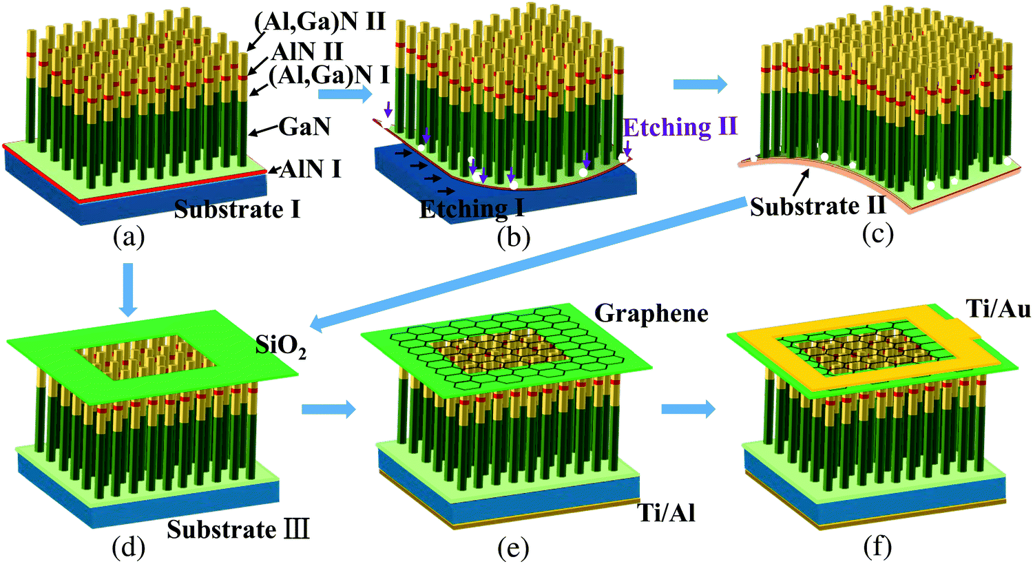
As illustrated in Fig. 1a, molecular beam epitaxy (MBE) was utilized to prepare (Al,Ga)N NWs on n-type Si(111) substrates. Prior to the MBE growth, the Si substrates (Substrate I) should be heated up to 900 °C for 15 min to eliminate native oxides in the growth chamber. The 7 × 7 reconstruction was normally observed after this treatment, indicating a clean surface. The sample was grown in the growth chamber with standard effusion cells for Ga, Al, and an N plasma cell. Initially, an AlN buffer layer (AlN I) was grown with a nominal Al flux of ∼3.0 nm min−1 for 1.0 min, which can be used to improve the NW orientation by preventing NW twist and tilt. Subsequently, GaN nanowires were grown with a Ga flux of ∼3.0 × 10⁻⁸ Torr for 100 min with a substrate temperature of 770 °C. Via Stranski–Krastanow growth mode, GaN deposited on partially relaxed AlN surface forming into islands. Due to strain minimization, these islands are expected to be preferential sites for further self-assembly GaN growth.9 After that, an (Al,Ga)N segment [(Al,Ga)N I] was grown for 30 min with a constant substrate temperature. Then, the AlN segment (AlN II) was grown for 4 min with an Al flux of 1.5 × 10⁸ torr. Finally, an (Al,Ga)N segment [(Al,Ga)N II] was grown for 60 min. During the processes of growing (Al,Ga)N segments, the nominal Al/Ga ratio was unchanged and kept at 3/2. The substrate temperature mentioned here refers to the thermocouple reading on the backside of the substrate. To increase the NW uniformity, samples were rotated with a rate of 120° s−1 during the growth process.
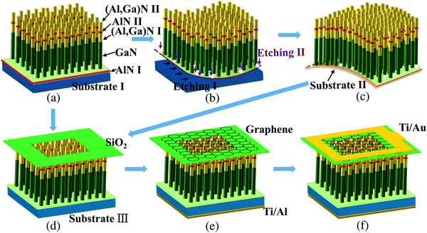 |
| | Fig. 1 Schematic illustration of fabricating the lift-off NW film and UV photodetector. (a) MBE growth of (Al,Ga)N NWs. (b) Use the EC etching to detach (Al,Ga)N NW film from the original substrate (Substrate I). (c) Transfer the NW film to a foreign substrate (Substrate II). (d) Deposit and selectively etch the SiO2 dielectric layer. (e) Deposit the Ti/Al back electrode and transfer the graphene. (f) Fabricate the Ti/Au front electrode. | |
Lift-off procedure of (Al,Ga)N NW films
First, the as-grown (Al,Ga)N NW sample was divided into pieces with size 10 × 10 mm2. Then these pieces were successively cleaned in acetone for 10 min and in isopropyl alcohol solution for 10 min. After drying, In/Au/Al alloys was melted on the back side of Si substrate by a welding torch. These electric contacts were also coated by epoxy resin to avoid EC corrosion. As shown in Fig. S1 (a schematic of the setup in the ESI†), the H-type cell without UV illumination was used for EC etching. The NW sample and Cu plate were used as the working electrode and counter electrode, respectively. During the EC etching, both electrodes were immersed in 1 M potassium hydroxide (KOH) or nitric acid (HNO3). After a certain time under an applied voltage, the (Al,Ga)N NWs were expected to be removed from the original Si substrate (Fig. 1b and c). Under the same applied voltage, the KOH solution used a much less time (∼2.5 min) to detach (Al,Ga)N NW film than HNO3 solution (∼8.5 min). More details of EC etching can be found in ref. 25.
Fabrication of UV photodetectors
Fig. 1d shows that a thick SiO2 layer was deposited and selectively etched on the top of NW array. Next, the back of Si substrate was deposited Ti/Al (50/200 nm) by electron beam evaporation. After that, the graphene on copper foil was transferred onto the NW array by wet transfer (Fig. 1e). The graphene is transparent in both UV and visible range, which can act as a current collecting layer in photodetectors. Finally, Ti/Au (50/200 nm) was deposited on the graphene as the front electrode by electron beam evaporation (Fig. 1f). To improve ohmic contact, the samples were annealed by the rapid thermal process at 400 °C for 30 min under N2 atmosphere. More details of the procedure of device fabrication can be found in ref. 9.
Characterization and measurements
To study the underlying processes of lift-off procedure and UV photodetectors systematically, five samples with different parameters were designed and prepared (Table 1). The as-grown (Al,Ga)N NWs was regarded as sample A. After using the KOH and HNO3 solutions to etch sample A (Fig. 1b and Fig. S1, ESI†), the detached NW films were regarded as samples B and C, respectively. Lastly, UV photodetectors based on samples A and C were marked as samples A1 and C1, respectively.
Table 1 Overview of the NW samples used for this work
| Sample |
(Al,Ga)N parameters |
UV photodetector |
| Sample A |
As-grown NWs |
No |
| Sample B |
NWs + KOH EC etching |
No |
| Sample C |
NWs + HNO3 EC etching |
No |
| Sample A1 |
NWs + Device fabrication |
Yes |
| Sample C1 |
NWs + HNO3 EC etching + Device fabrication |
Yes |
All NW samples were characterized by scanning electron microscopy (SEM, S-4800, Hitachi). The scanning transmission electron microscopy (STEM, Talos F200x, FEI) and high-resolution energy dispersive X-ray (EDX) mapping were utilized to measure the morphology and element distribution of NWs. The STEM samples were prepared by focused ion beam (FIB, Scios, FEI). Atomic force microscopy (AFM, Dimension ICON, Bruker) was utilized to study the surface roughness, and X-ray photoelectron spectroscopy (XPS, PHI 5000 Versaprobe III, ULVAC-PHI) was performed to study the chemical state of the samples. To study the surface states and surface potentials of NW films, a scanning Kelvin probe force microscopy (KPFM) was utilized. Moreover, photoluminescence (PLE-2355 test system) and spectrophotometer (LAMBDA 750) measurements were conducted to study the optical properties. The current–voltage and transient responses characteristics of the photodetectors were measured by the Agilent probe station (Agilent B1500A, Agilent, USA) and a commercial 275 nm light-emitting diode (LED). The spectral response measurement employed a self-constructed photoelectric measurement system. The responsivity was measured at −2 V with a SolarSimulator (ABET Technologies, USA).
Results and discussion
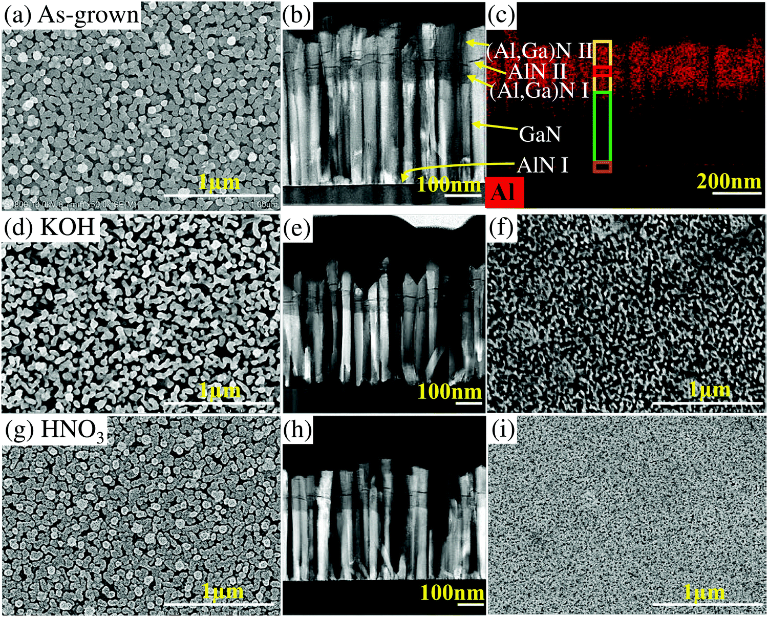
As shown in Fig. 2a and b, the well vertically aligned (Al,Ga)N NWs of sample A exhibit a uniform dense arrangement on Si substrate. The NW diameter and height are about 55 nm and 475 nm, respectively. Furthermore, the EDX mapping in Fig. 2c shows the Al element exists in the top of NWs, agreeing with the epitaxial design. As illustrated in Fig. 2d and e, the average NW diameter and height of sample B are decreased to about 46 nm and 414 nm, respectively. The space among NWs of sample B is much larger than that of sample A. From Fig. 2g and h, the (Al,Ga)N NWs of sample C have the similar space among NWs with that of sample A. After HNO3 etching, the NW diameter of sample C is about 51 nm and the NW height is about 422 nm. The netlike GaN parasitic layers at the bottom NWs are significant for the NW films as they are used to connect all NWs.25 It is clearly illustrated in Fig. 2f and i that the size of openings within the parasitic layer of sample B is much larger than that of sample C. That means the KOH solution can etch more GaN materials than the HNQ3 solution. Moreover, the gap of sample B (Fig. 2e) between the NW film and foreign substrate is much larger than that of sample C (Fig. 2h). Besides the gap, the evenness of GaN parasitic layer of sample B is worse than that of sample C. Compared to those of sample B, the more flat bottom layer with a smaller gap can achieve the ohmic contact much more easily, which is significant for improving device performance.
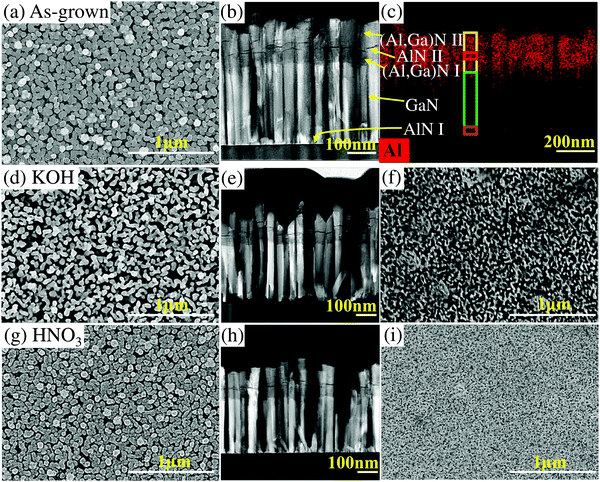 |
| | Fig. 2 (a) Plan-view SEM image, (b) side-view STEM image and (c) EDX mapping of sample A. (d) Plan-view SEM image of the top of NW film and (e) side-view STEM image of NWs of sample B. (f) Plan-view SEM image of the bottom of NW film of sample B. (g) Plan-view SEM image of the top of NW film and (h) side-view STEM image of NWs of sample C. (i) Plan-view SEM image of the bottom of NW film of sample C. | |
Fig. 2 shows that the NWs can be lifted off by both KOH and HNO3. Fig. S2a (ESI†) demonstrates that a bottom AlN layer (AlN I) exists between the GaN segment and Si substrate before EC etching (sample A). However, after the EC etching by KOH or HNO3 solutions, the (Al,Ga)N NW films can be detached successfully and very limited AlN remained under the GaN segment (Fig. S2b and c, ESI†). Therefore, the thin bottom AlN buffer layer (AlN I) plays a key role in the lift-off process, which acts as a sacrificial layer. As illustrated in Fig. 3, two etching pathways (Etching I and Etching II) exist during the EC etching of sample A. The etching solution can reach the bottom AlN layer through defects and openings in the bottom GaN layer. Once AlN I layer is etched from the top, horizontal under-etching of the GaN layer sets in, which results in the netlike shape of bottom GaN layer (Fig. 2f and i). The etching times in this work are longer than that used in ref. 25, which could mainly attributed to the bottom GaN layer. In other words, the size and density of the defects and openings within the bottom GaN layer may be smaller than those in ref. 25, leading to the longer etching time. The relevant chemical etchings occur via the following reactions.27–29
| | | 2AlN + 3H2O → Al2O3 + 2NH3 | (1) |
| | | AlN + 3H2O → Al(OH)3 + NH3 | (2) |
| | | 2GaN + 3H2O → Ga2O3 + 2NH3 | (3) |
| | | GaN + 3H2O → Ga(OH)3 + NH3 | (4) |
When applied a bias voltage on the EC setup, the reactions can be accelerated. The Gibbs free energies (Δ
Gr) of the above reactions are calculated based on KOH to be about (1) −350.1 kJ mol
−1, (2) −334.2 kJ mol
−1, (3) 1399.9 kJ mol
−1 and (4) 723.5 kJ mol
−1, respectively.
28,29 Hence, the formation of Al
2O
3 and Al(OH)
3 is much easier than that of Ga
2O
3 and Ga(OH)
3. Furthermore, the dissolution of Al
2O
3 and Al(OH)
3 in electrolyte was reported to be much faster than that of Ga
2O
3 and Ga(OH)
3.
27–29 Thus, AlN is selectively etched compared to GaN. In other words, the AlN layer can be etched quickly within KOH solution, while the GaN section is etched slowly. As Al atoms have a shorter diffusion mean free path, the diffusion of Al atoms are limited with respect to Ga, resulting in a large number of Al atoms may accumulate near the NW sidewalls. Hence, an Al-rich (Al,Ga)N shell can be formed on the NW lateral surfaces.
11,30 We propose that the etching rate of (Al,Ga)N has a high probability to be lower than that of AlN but larger than that of GaN. The etching rate of Al-rich (Al,Ga)N could be close to that of AlN. Thus, it is proposed that Al-rich (Al,Ga)N shell could be etched for both samples B and C after the EC etching, which is schematically illustrated in
Fig. 3. Furthermore, (Al,Ga)N NWs are normally core–shell structures.
11,30 As the upper AlN layers (AlN II in
Fig. 2e and h) remain well, the upper (Al,Ga)N shell [(Al,Ga)N II] should still remain after the EC etching.
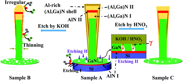 |
| | Fig. 3 Schematic illustration of the different pathways for the etching processes leading to the detached NW films of samples B and C. | |
In addition, the etching selectivity of AlN over GaN of KOH solution is much higher than those of many other acid solutions, including HNO3.27 Thus, HNO3 needs more etching time than KOH to detach (Al,Ga)N NWs under the same EC conditions. However, compared to those of sample B (Fig. 2), the NW evenness of sample C is much better and the NW diameters of sample C remain more stable after the EC etching. Therefore, although HNO3 (sample C) needs the longer etching time than KOH (sample B), HNO3 etches much less (Al,Ga)N NWs than KOH. For the underlying mechanism, we mainly attribute to the hydrophobicity of the bottom GaN layer, which is schematically shown as the red “γ” in the enlarged part of Etching II in Fig. 3. The pathway Etching II plays a more important role than Etching I during the EC etching process.25 However, as the defects and openings in the bottom GaN layer are very small (Fig. 2i), the KOH or HNO3 solutions need a long time to reach the AlN layer (AlN I) through them because of the hydrophobicity. If the size of defects and openings is too small to resist penetrating, the KOH or HNO3 solutions should need more time to etch GaN to enlarge the size firstly, then penetrate inside to etch the bottom AlN layer. In the duration before reaching AlN, KOH can etch much more (Al,Ga)N NWs than HNO3 because of the higher etching rate. As a result, HNO3 is better than KOH for the lift-off procedure of (Al,Ga)N NWs. For choosing etching solutions, apart from the selectively etching rate of AlN over GaN, the protection of NWs during the detaching process should be taken into consideration as another key factor.
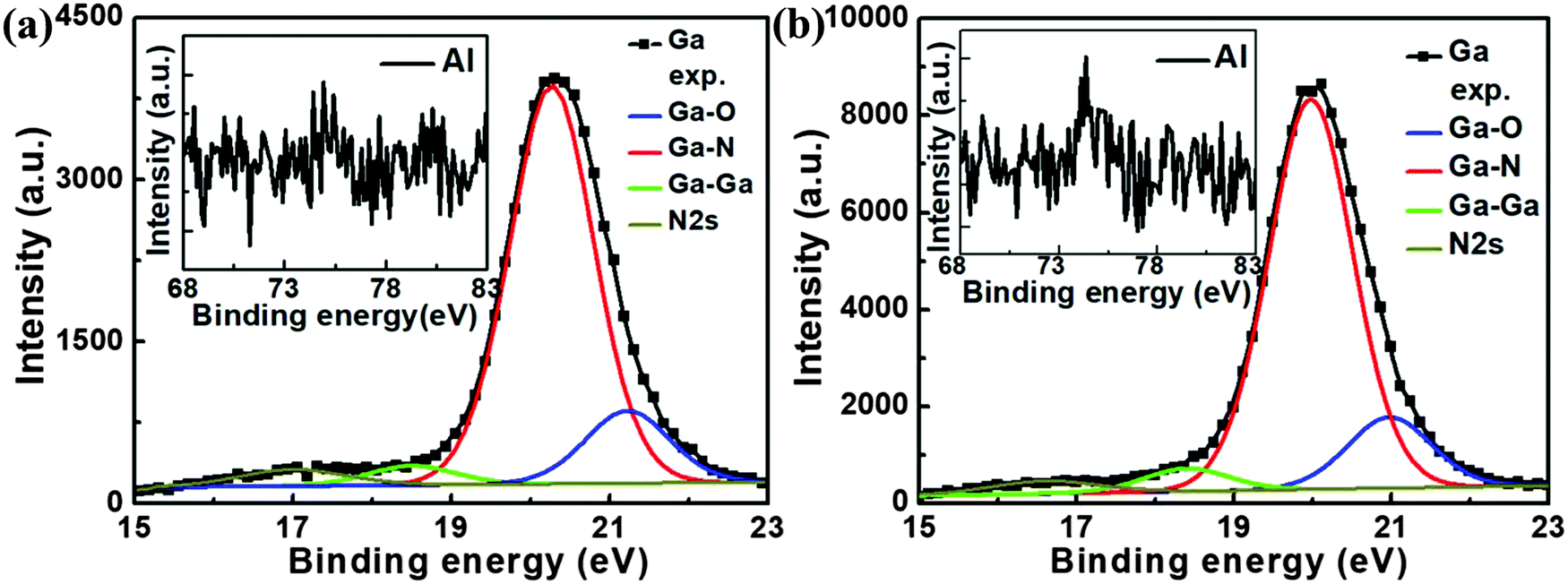
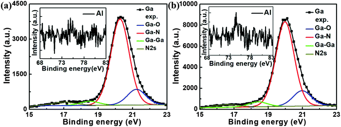
In order to further study the chemical state of the lift-off NW films, the XPS spectra around the Ga (3d) and Al (2p) core levels were measured from the bottom side of samples B and C. The experimental Ga (3d) XPS data were fitted by four components, corresponding to the bonds Ga–O, Ga–N, Ga–Ga and N 2s.12,31–36 More fitting details, including binding energies, are summarized in Fig. 4 and Table 2. The XPS spectra for the Al (2p) core level region (insets in Fig. 4) illustrate that no signals of Al element are detected, which means very little AlN or Al2O3 remained in the detached NW films. The results are in good agreement with those in Fig. S2 (ESI†). Hence, almost all AlN materials were etched and the reactants [Al2O3, Al(OH)3] were dissolved into the etching solution. The dominating component is GaN, indicating that chemical reactions have a limited impact on the NW films. As expected by the presumed chemical reactions, the second strongest component is Ga2O3. Moreover, positive shift of Ga (3d) in XPS spectra can be caused by the damaged crystal lattice.35Fig. 4 and Table 2 clearly illustrate that the binding energies of four components obtained from the sample B are all larger than those of sample C. Therefore, compared to that etched by KOH, the crystal quality of the NW film etched by HNO3 is likely to be better.
 |
| | Fig. 4 XPS spectra of Ga (3d) and Al (2p) (inset) for (a) sample B and (b) sample C. | |
Table 2 Fitting details for the Ga (3d) XPS spectra of samples B and C
| Binding energy (eV) |
Sample B |
Sample C |
Difference (sample B − sample C) |
| Ga–O |
21.23 |
20.98 |
0.25 |
| Ga–N |
20.27 |
19.98 |
0.29 |
| Ga–Ga |
18.5 |
18.4 |
0.1 |
| N2s |
17.0 |
16.6 |
0.4 |
As shown in Fig. S3 (ESI†), the root-mean-square roughness (RMS) results of samples A–C are 36.1 nm, 37.6 nm and 37.0 nm, respectively, indicating that the EC etching process can change the NW surface morphology. The RMS of sample C is smaller than that of sample B, which agrees with the TEM data in Fig. 2e and h. Due to a larger RMS, the (Al,Ga)N NWs are etched more seriously in KOH (sample B) than those etched in HNO3 (sample C), which further demonstrates the schematic illustration of Fig. 3.
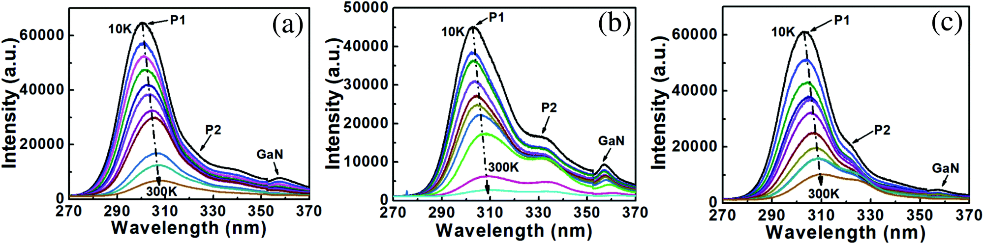
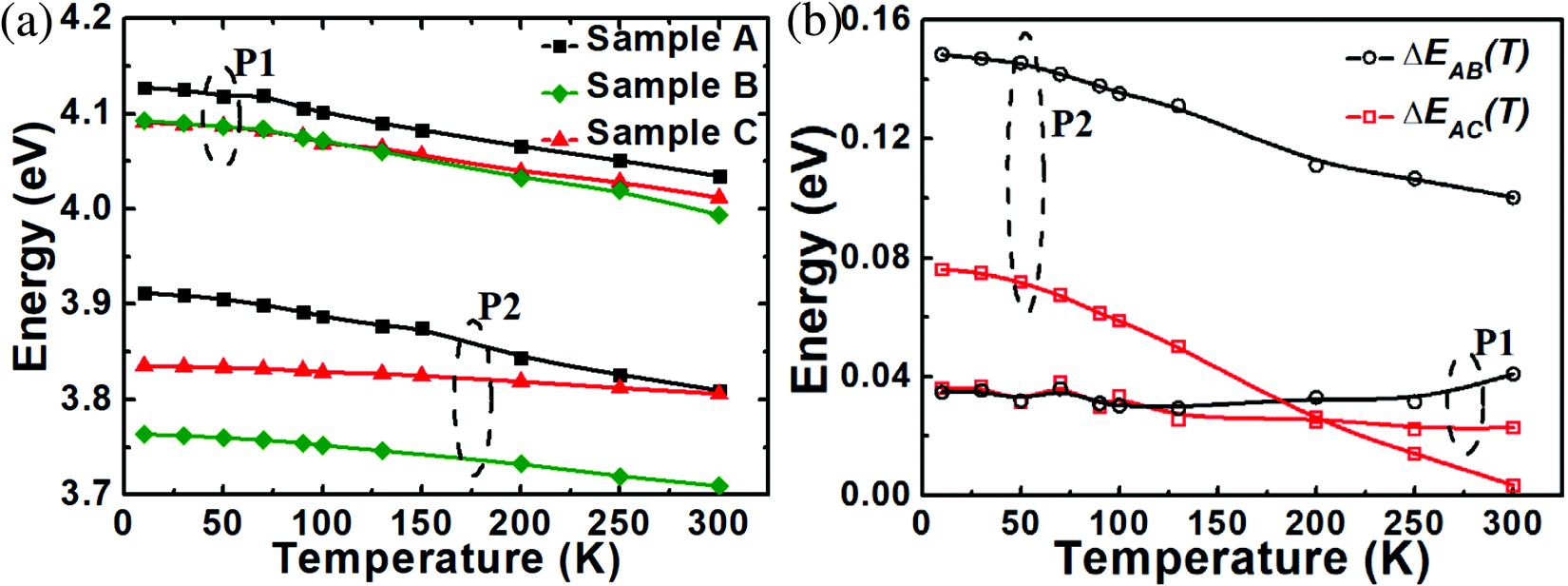
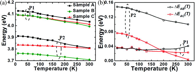
Fig. 5 shows the temperature-dependent PL results of samples A–C performed from 10 K to 300 K by a 213 nm laser. The peak shifts of all three samples with temperature decreasing owing to the bandgap shrinkage effect.26,37–39 An energy peak at about ∼358 nm can be clearly seen, which comes from the GaN at the lower parts of NWs. The PL spectra of sample A have asymmetric shapes with low energy tails, which indicate they are mainly dominated by the radiative recombination of localized excitons.37 By the multimodal Lorenz fitting, the PL spectra can be divided into two peaks, a left peak of the dominated band (P1) and a right peak (P2).26 Different NW diameters could have different impacts on the diffusion and desorption of Al atoms, which could result in the compositional fluctuation exists among NWs with different diameters.25,40–42 Hence, NWs with different diameters can emit photons with different wavelengths. The PL spectrum of sample A measured at 10 K still has P1 and P2. As a result, both two peaks of sample A are assigned to come from (Al,Ga)N NWs with different diameters, not defects. It is clearly shown in Fig. 2 that the NWs of sample B have been etched much more than those of sample C, leading to the more serious diameter fluctuation of sample B. Therefore, the P2 of sample B are the most obvious among those of samples A–C.
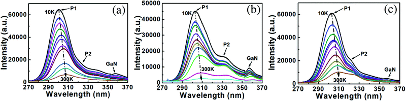 |
| | Fig. 5 Temperature-dependent PL spectra of (a) sample A, (b) sample B and (c) sample C. | |
Compared to the P1 and P2 of sample A, those of both samples B and C show a redshift after the EC etching (Fig. 6a). To further study the energy differences of peak photons, we calculate ΔEAB(T) and ΔEAC(T) as follows:
| | | ΔEAB(T) = Eg,A(T) − Eg,B(T) | (5) |
| | | ΔEAC(T) = Eg,A(T) − Eg,C(T) | (6) |
where
Eg,A(
T),
Eg,B(
T) and
Eg,C(
T) are the PL peak energies of samples A, B and C at
T K, respectively. As clearly illustrated in
Fig. 6b, for P2, Δ
EAC(
T) is always smaller than Δ
EAB(
T) from 10 K to 300 K. For P1, Δ
EAC(
T) is comparative to Δ
EAB(
T) at low temperatures, while it becomes smaller with temperature increasing. Such PL redshifts could mainly result from the removal of Al-rich (Al,Ga)N shells, which agrees with the above hypothesis (
Fig. 3). As a result, compared to sample B, sample C is etched less under the EC etching process. It further demonstrates that HNO
3 is better than KOH to protect (Al,Ga)N NWs during the EC etching process.
 |
| | Fig. 6 (a) Temperature-dependent variation of PL peaks. (b) Energy difference of PL peaks. | |
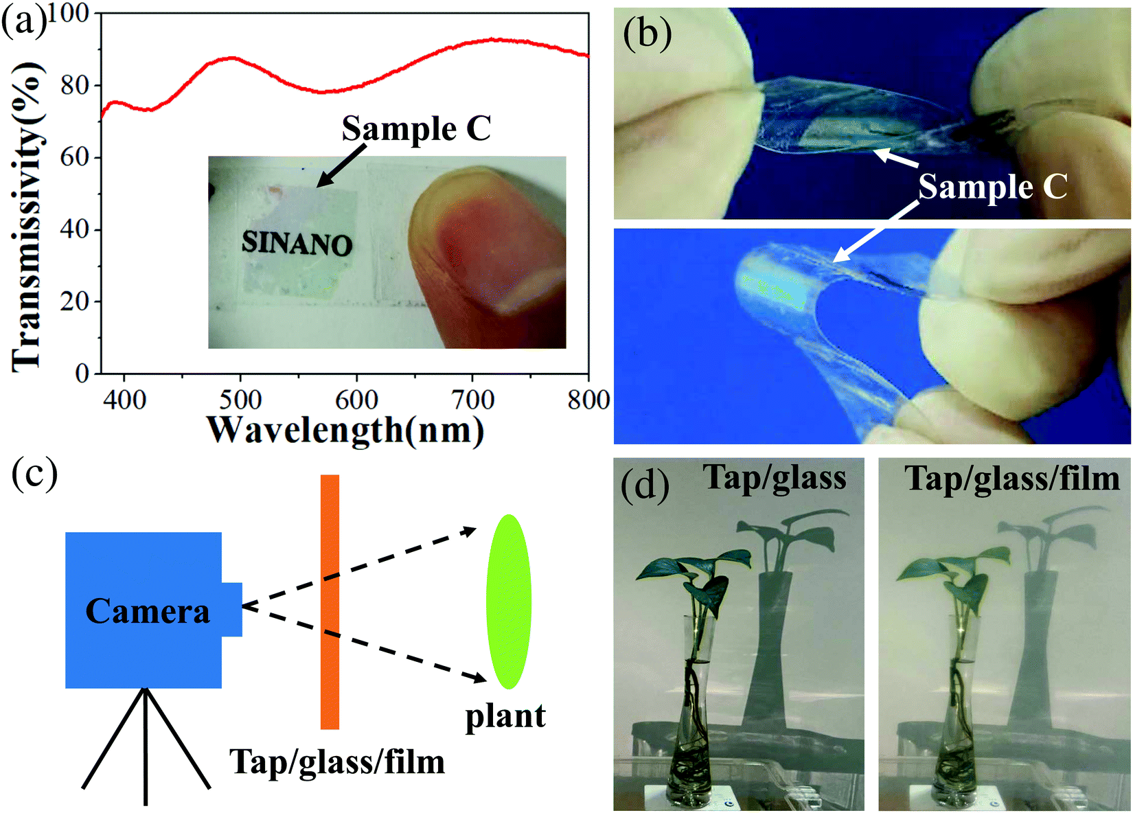
According to above results and discussion, sample C is better than sample B for device fabrication because of two reasons: (Al,Ga)N NWs of sample C are etched less, and the more flat bottom GaN layer is better to achieve ohmic contact. To study its flexibility and transmissivity, sample C was transferred on a transparent adhesive tape. As clearly illustrated in the inset to Fig. 7a, when sample C (10 × 10 mm2) is put on the top of a piece of paper with the writing “SINANO”, the writing is clearly visible. The highest transmissivity of sample C without tape can reach 93% and it is much higher than that (82.2%) in ref. 25. In the full visible range from 380 nm to 800 nm, the transmissivity is always larger than 71%, which indicates that such NW film can be used as a material for semi-invisible semiconductors.25,43 Furthermore, sample C still kept its structural integrity well after hundreds of bends with an angle over 180 degrees (Fig. 7b), which mainly originates from the NW structure and the netlike thin connecting layer. To intuitively demonstrate the transparency, we use a camera as Fig. 7c to take pictures and a video (Video S1 of the ESI†) through sample C. As clearly illustrated in Fig. 7d, no obvious changes are obtained between the two images with and without sample C. Therefore, sample C could be a candidate material for fabricating the invisible devices mentioned in ref. 25.
 |
| | Fig. 7 (a) Transmission spectrum of sample C. The inset shows a photograph of sample C placed on a transparent tape on top of a piece of paper with the writing “SINANO”. (b) Optical images of sample C under high bending. (c) Schematic of the set for taking images of a plant through sample C on a tap and a glass. (d) Optical images of a plant through the tap/glass with and without sample C. “Tap/glass” means a tap is on a glass and “Tap/glass/film” represents sample C is on the “Tap/glass”. | |
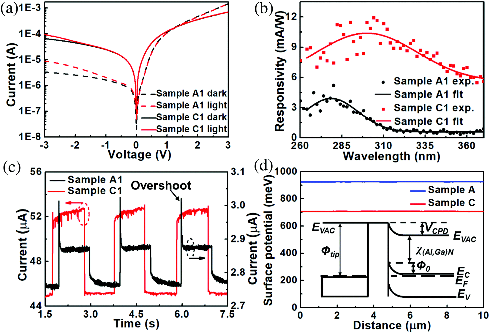
To study the photoelectric response of detached (Al,Ga)N NWs, samples A1 and C1 were fabricated based on the NW films of samples A and C, respectively. As shown in Fig. 8a, both logarithmic I–V curves of samples A1 and C1 display a typical rectification property. At the bias of −3 V, the dark current of sample A1 is 3.4 μA and that of sample C1 is 65.4 μA. The photocurrents under 275 nm illumination are 8.9 μA (sample A1) and 95.2 μA (sample C1). The corresponding photo-to-dark current ratios of samples A1 and C1 at 275 nm are around 2.6 and 1.5, respectively. In addition, as an essential parameter to assess the UV detector performance, the responsivity was characterized under the action of the unit incident radiation power.9,44 As illustrated in Fig. 8b, by fitting the experimental data, a peak responsivity of sample C1 (foreign Si substrate) is about 10.4 mA W−1 at 300 nm, while that of sample A1 is around 3.9 mA W−1 at 279 nm. Thus, the peak responsivity of the (Al,Ga)N NWs is enhanced by about 166% after the HNO3 treatment. The increased wavelength of peak response of sample C1 mainly results from the removal of Al-rich (Al,Ga)N shell after the EC etching.
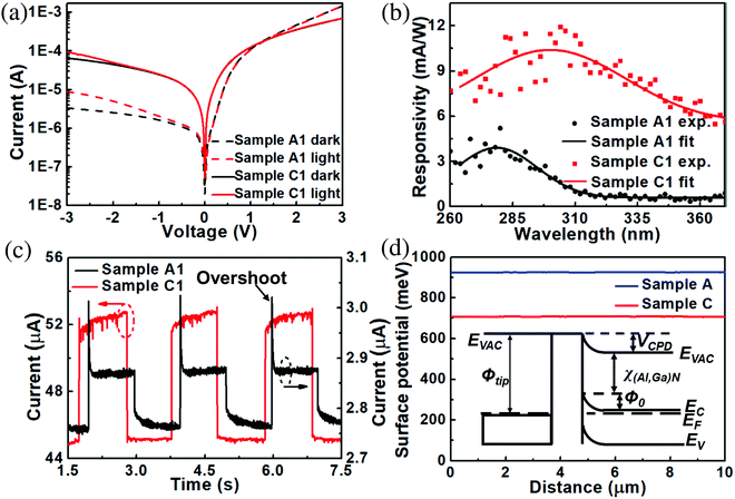 |
| | Fig. 8 (a) I–V characteristics of the samples A1 and C1 in the dark and 275 nm light illumination. (b) Spectral responses and (c) response times of samples A1 and C1 at the bias of −2 V. (d) The surface potential distribution curves of samples A and C. The inset in (d) is the schematic band diagram of KPFM. | |
In Fig. 8c, the on/off switching behaviors of both detectors appear alternately according to the periodic illuminations, indicating that the detectors have the reproducibility and stability. To quantitatively assess the transient response of samples, the rise time (τon) is defined as the time when the current increases to 90% of the maximum photoresponse current, and the decay time (τoff) is defined as the time when the current drops to 10% of the maximum photoresponse current.9,44,45 For better accuracy, three points were extracted to calculate the average data of response time. For sample A1, τon = <4 ms and τoff = ∼140 ms, while for sample C1, τon = ∼65 ms and τoff = <4 ms. 4 ms is the precision of equipment we used. In order to better compare with some recent novel photodetectors, Table 3 lists the key parameters. By comparison, sample C1 has the advantages in the transient response.
Table 3 Comparison of response time between this work and some state-of-the-art reports
| Materials |
Wavelength (nm) |
τ
on/τoff (ms) |
Ref. |
| Detached (Al,Ga)N NW film |
275 |
65/<4 |
This work |
| As-grown (Al,Ga)N NWs |
360 |
4000/4700 |
9
|
| p-CuZnS/n-TiO2 |
350 |
450/410 |
50
|
| 2D perovskite Sr2Nb3O10 |
270 |
0.4/40 |
51
|
| CH3NH3PbI3/β-Ga2O3 wafer |
254 |
110/450 |
52
|
| β-Ga2O3 nanomembrane |
252 |
4000/24000 |
53
|
| Electrospun TiO2 film |
350 |
2270/2540 |
54
|
To study the underlying mechanism of photoelectric response, KPFM was utilized to measure the surface potentials (VCPD) of NW films. From Fig. 8d, the VCPD of sample C is about 708 meV, which is much lower than that of sample A (around 925 meV). Hence, the EC etching by HNO3 can reduce the surface potential of (Al,Ga)N NWs significantly. VCPD is related to the work function difference between a metal tip and the (Al,Ga)N NW surface, which can be expressed as follow:46–49
| | | eVCPD = ϕtip − ϕ(Al,Ga)N = ϕtip − χ(Al,Ga)N − ϕ0 − (EC − EF) | (7) |
where
ϕtip and
ϕ(Al,Ga)N are the work functions of metal tip and (Al,Ga)N NWs, and
χ(Al,Ga)N is the electron affinity of (Al,Ga)N NWs.
ϕ0 is the surface band bending.
Ec and
EF are the conduction band edge and the Fermi level of (Al,Ga)N materials, respectively. When
ϕtip,
χ(Al,Ga)N,
Ec and
EF are assumed to be constant, the variation of
VCPD is mainly related to
ϕ0, which depends on the sign and quantity of surface charge, as well as the distribution and density of surface states.
46 Thus, compared to that of sample A, the lower
VCPD of sample C mainly results from the larger
ϕ0, which may be beneficial for the diffusions of carriers and lower surface states.
As illustrated in Fig. 8c, the current overshoots only when switching on UV light, indicating an instantaneous accumulation of photogenerated electrons/holes on the NW surfaces. With no proper potential to drive carriers to flow towards opposite directions, the part of them will subsequently lost via the nonradiative transition and radiative recombine. After that, the photocurrent decays until a stationary photocurrent is reached.50,55 Thus, such photocurrent overshooting feature mainly contributes to the rapid rise time of sample A1. To further study the underlying mechanism, the energy band diagrams of samples A1 and C1 are plotted in Fig. 9. The EC etching can remove the Al-rich (Al,Ga)N shell and the bottom AlN layer (AlN I) of sample C1, which could decrease the barriers and accelerate the carrier diffusions. The decreased VCPD of sample C1 (Fig. 8d) could further decrease the barriers or surface states. Compared to sample A1 at the same bias, the decrease of barriers of sample C1 has the possibility to eliminate the photocurrent overshooting feature. In addition, the elimination of surface states via EC etching can suppress non-radiative surface recombination, resulting in that more carriers can reach the metal and graphene electrodes.11,56 Surface defects of sample A1, such as the surface dangling bonds, can capture the photon-generated electron–hole pairs to deteriorate the responsivity.11 As a result, the EC etching is beneficial to decrease the barriers, the surface states and defects, which mainly contribute to the higher responsivity and faster decay response of sample C1 (Fig. 8).
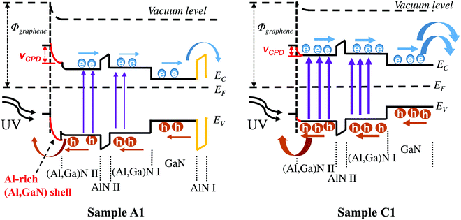 |
| | Fig. 9 Schematic illustration of energy band diagrams for samples A1 and C1. The wider arrows represent more carriers. | |
Conclusion
In conclusion, we have proposed and experimentally demonstrated the novel technology of detaching (Al,Ga)N NW films from their growth substrates. The approach has the advantages of low cost and easy operation. It is found that HNO3 is better than KOH for this lift-off technology. Besides the ability of selectively etching, the HNO3 solution can also protect the (Al,Ga)N NWs without too much etching during the detaching process. After the lift-off procedure, the detached (Al,Ga)N NW films are highly transparent and exhibit good flexibility. Furthermore, after the HNO3 etching, the photoelectric response of the (Al,Ga)N NW film can be improved significantly. By comparing the UV photodetectors with to without HNO3 etching, the peak responsivity is enhanced by about 166% and the decay time becomes much faster. By systematical analyses, some reasons contribute to the significant improvements, such as the removal of the bottom AlN layer and Al-rich (Al,Ga)N shell, the decrease of the surface states and defects. Therefore, such (Al,Ga)N NW films are promising for various fields with high requirements of flexibility and/or transparency, including detectors and super-flexible intelligent skin.
Conflicts of interest
There are no conflicts to declare.
Acknowledgements
The authors are grateful for National Key Research and Development Program of China (No. 2018YFB0406602), Natural Science Foundation of Jiangsu Province (No. BK20180252), Key Research Program of Frontier Sciences, CAS (No. ZDBS-LY-JSC034), and National Natural Science Foundation of China (No. 61804163 and 61875224). The authors also would like to acknowledge the support from Natural Science Foundation of Jiangxi Province (No. 20192BBEL50033), Research Program of Scientific Instrument and Equipment of CAS (No. YJKYYQ20200073) and SINANO (No. Y4JAQ21001). We are thankful for the technical support from Vacuum Interconnected Nanotech Workstation (Nano-X, No. B2006), Platform for Characterization & Test of SINANO, CAS.
Notes and references
- N. Guan, X. Dai, A. V. Babichev, F. H. Julien and M. Tchernycheva, Chem. Sci., 2017, 8, 7904–7911 RSC.
- N. Aggarwal and G. Gupta, J. Mater. Chem. C, 2020, 8, 12348–12354 RSC.
- S.-J. Tsai, C.-L. Wu, N.-T. Tsai, S.-S. Wong and L.-W. Tu, Carbon, 2018, 130, 390–395 CrossRef CAS.
- J.-H. Oh and J.-W. Park, Phys. Status Solidi RRL, 2020, 14, 1900707 CrossRef CAS.
- T.-H. Yeh, C.-C. Lee, C.-J. Shih, G. Kumar, S. Biring and S.-W. Liu, Org. Electron., 2018, 59, 266–271 CrossRef CAS.
- D. Kim, S. S. Shin, S. M. Lee, J.-S. Cho, J. H. Yun, H. S. Lee and J. H. Park, Adv. Funct. Mater., 2020, 30, 2001775 CrossRef CAS.
- M. Spies and E. Monroy, Semicond. Sci. Technol., 2019, 34, 053002 CrossRef CAS.
- Y. Zhao, F. Yun, L. Feng, S. Wang, Y. Li, X. Su, M. Guo, W. Ding and Y. Zhang, IEEE Access, 2017, 5, 11712–11716 Search PubMed.
- M. Zhou, H. Qiu, T. He, J. Zhang, W. Yang, S. Lu, L. Bian and Y. Zhao, Phys. Status Solidi A, 2020, 217, 2000061 CrossRef CAS.
- J. He, Y. Zhong, Y. Zhou, X. Guo, Y. Huang, J. Liu, M. Feng, Q. Sun, M. Ikeda and H. Yang, Appl. Phys. Express, 2019, 12, 055507 CrossRef CAS.
- H. Sun, M. K. Shakfa, M. M. Muhammed, B. Janjua, K.-H. Li, R. Lin, T. K. Ng, I. S. Roqan, B. S. Ooi and X. Li, ACS Photonics, 2018, 5, 964 CrossRef CAS.
- R. Huang, T. Liu, Y. Zhao, Y. Zhu, Z. Huang, F. Li, J. Liu, L. Zhang, S. Zhang, D. An and H. Yang, Appl. Surf. Sci., 2018, 440, 637–642 CrossRef CAS.
- T. He, Y. Zhao, X. Zhang, W. Lin, K. Fu, C. Sun, F. Shi, X. Ding, G. Yu, K. Zhang, S. Lu, X. Zhang and B. Zhang, Nanophotonics, 2018, 7, 1557–1562 CAS.
- L. Liu, F. Lu and J. Tian, Appl. Surf. Sci., 2020, 508, 145250 CrossRef.
- A. Fernando-Saavedra, S. Albert, A. Bengoechea-Encabo, D. Lopez-Romero, M. Niehle, S. Metzner, G. Schmidt, F. Bertram, M. A. Sanchez-Garcia, A. Trampert, J. Christen and E. Calleja, J. Cryst. Growth, 2019, 525, 125189 CrossRef CAS.
- X. Zhang, B. Liu, Q. Liu, W. Yang, C. Xiong, J. Li and X. Jiang, ACS Appl. Mater. Interfaces, 2017, 9, 2669–2677 CrossRef CAS.
- Z. Xu, S. Zhang, J. Liang, J. Lin, Y. Yu, R. Li, F. Gao and G. Li, J. Power Sources, 2019, 419, 65–71 CrossRef CAS.
- L. Feng, Y. Li, H. Xiong, S. Wang, J. Wang, W. Ding, Y. Zhang and F. Yun, Appl. Phys. Express, 2016, 9, 081003 CrossRef.
- C.-H. Lee, Y.-J. Kim, Y. J. Hong, S.-R. Jeon, S. Bae, B. H. Hong and G.-C. Yi, Adv. Mater., 2011, 23, 4614 CrossRef CAS.
- G. Lupina, J. Kitzmann, I. Costina, M. Lukosius, C. Wenger, A. Wolff, S. Vaziri, M. Ostling, I. Pasternak, A. Krajewska, W. Strupinski, S. Kataria, A. Gahoi, M. C. Lemme, G. Ruhl, G. Zoth, O. Luxenhofer and W. Mehr, ACS Nano, 2015, 9, 4776–4785 CrossRef CAS.
- X. Dai, A. Messanvi, H. Zhang, C. Durand, J. Eymery, C. Bougerol, F. H. Julien and M. Tchernycheva, Nano Lett., 2015, 15, 6958–6964 CrossRef.
- C. Ramesh, P. Tyagi, S. Gautam, S. Ojha, G. Gupta, M. S. Kumar and S. S. Kushvaha, Mater. Sci. Semicond. Process., 2020, 111, 104988 CrossRef CAS.
- G. Calabrese, P. Corfdir, G. Gao, C. Pfueller, A. Trampert, O. Brandt, L. Geelhaar and S. Fernandez-Garrido, Appl. Phys. Lett., 2016, 108, 202101 CrossRef.
- P. Tyagi, C. Ramesh, J. Kaswan, S. Dhua, S. John, A. K. Shukla, S. C. Roy, S. S. Kushvaha and S. K. Muthusamy, J. Alloys Compd., 2019, 805, 97–103 CrossRef CAS.
- Y. Zhao, Z. Xing, L. Geelhaar, J. Zhang, W. Yang, T. Auzelle, Y. Wu, L. Bian and S. Lu, ACS Appl. Nano Mater., 2020, 3, 9943–9950 CrossRef CAS.
- J. He, S. Wang, J. Chen, F. Wu, J. Dai, H. Long, Y. Zhang, W. Zhang, Z. C. Feng, J. Zhang, S. Du, L. Ye and C. Chen, Nanotechnology, 2018, 29, 195203 CrossRef.
- D. Zhuang and J. H. Edgar, Mater. Sci. Eng., R, 2005, 48, 1–46 CrossRef.
- W. Guo, R. Kirste, I. Bryan, Z. Bryan, L. Hussey, P. Reddy, J. Tweedie, R. Collazo and Z. Sitar, Appl. Phys. Lett., 2015, 106, 082110 CrossRef.
- D. S. Li, M. Sumiya, S. Fuke, D. R. Yang, D. L. Que, Y. Suzuki and Y. Fukuda, J. Appl. Phys., 2001, 90, 4219–4223 CrossRef CAS.
- A. Pierret, C. Bougerol, S. Murcia-Mascaros, A. Cros, H. Renevier, B. Gayral and B. Daudin, Nanotechnology, 2013, 24, 115704 CrossRef CAS.
- K. Li, A. T. S. Wee, J. Lin, Z. C. Feng and S. J. Chua, Mat. Res. Soc. Symp. Proc., 2000, 618, 303–308 CrossRef CAS.
- M. C. S. Escano, J. T. Asubar, Z. Yatabe, M. Y. David, M. Uenuma, H. Tokuda, Y. Uraoka, M. Kuzuhara and M. Tani, Appl. Surf. Sci., 2019, 481, 1120–1126 CrossRef CAS.
- M. Mishra, A. Gundimeda, S. Krishna, N. Aggarwal, B. Gahtori, N. Dilawar, V. V. Aggarwal, M. Singh, R. Rakshit and G. Gupta, Phys. Chem. Chem. Phys., 2017, 19, 8787–8801 RSC.
- R. Zhou, M. Feng, J. Wang, Y. Zhong, Q. Sun, J. Liu, Y. Huang, Y. Zhou, H. Gao, M. Ikeda, Z. Li, Y. Zhao, T. Liu and H. Yang, Solid-State Electron., 2020, 171, 107863 CrossRef CAS.
- C. Wang, M.-R. Zhang, W.-X. Song, H.-D. Peng, H. Huang, Z.-G. Wang, R. Xi and G.-B. Pan, Chem. Phys. Lett., 2018, 710, 54–58 CrossRef CAS.
- N. Karar, R. Opila and T. Beebe, Jr., J. Electrochem. Soc., 2011, 158, D342–D350 CrossRef CAS.
- J. Zeng, J. Yan, J. Wang, P. Cong, J. Li, S. Sun and Y. Tao, Phys. Status Solidi C, 2012, 9, 733–736 CrossRef CAS.
- H. Murotani, Y. Yamada, T. Taguchi, A. Ishibashi, Y. Kawaguchi and T. Yokogawa, J. Appl. Phys., 2008, 104, 053514 CrossRef.
- W. C. Ke, C. S. Ku, H. Y. Huang, W. C. Chen, L. Lee, W. K. Chen, W. C. Chou, W. H. Chen, M. C. Lee, W. J. Lin, Y. C. Cheng and Y. I. Cherng, Appl. Phys. Lett., 2004, 85, 3047–3049 CrossRef CAS.
- A. L. Bavencove, G. Tourbot, J. Garcia, Y. Desieres, P. Gilet, F. Levy, B. Andre, B. Gayral, B. Daudin and L. S. Dang, Nanotechnology, 2011, 22, 345705 CrossRef CAS.
- X. Zhang, B. Haas, J.-L. Rouviere, E. Robin and B. Daudin, Nanotechnology, 2016, 27, 455603 CrossRef.
- Y. Zhao, W. Yang, S. Lu, Y. Wu, X. Zhang, L. Bian, X. Li and M. Tan, J. Cryst. Growth, 2019, 514, 124–129 CrossRef CAS.
-
J. Y. Zhang, S. L. Lu, Y. K. Zhao and Z. W. Xing, CHN Pat., 202010517504.6, 2020 Search PubMed.
- T. He, X. Zhang, X. Ding, C. Sun, Y. Zhao, Q. Yu, J. Ning, R. Wang, G. Yu, S. Lu, K. Zhang, X. Zhang and B. Zhang, Adv. Opt. Mater., 2019, 7, 1801563 CrossRef.
- D.-S. Tsai, W.-C. Lien, D.-H. Lien, K.-M. Chen, M.-L. Tsai, D. G. Senesky, Y.-C. Yu, A. P. Pisano and J.-H. He, Sci. Rep., 2013, 3, 2628 CrossRef.
- M. A. Deeb, J. Wei, J. Hartmann, H.-H. Wehmann and A. Waag, Phys. Status Solidi A, 2015, 212, 732–735 CrossRef CAS.
- S. Lee, Surf. Sci., 2015, 641, 16–22 CrossRef CAS.
- K. K. Madapu, S. Parida, K. Jeganathan, M. Baral and S. Dhara, J. Appl. Phys., 2019, 125, 164308 CrossRef.
- M. E. Erkan, V. Chawla, I. Repins and M. A. Scarpulla, Sol. Energy Mater. Sol. Cells, 2015, 136, 78–85 CrossRef CAS.
- X. Xu, J. Chen, S. Cai, Z. Long, Y. Zhang, L. Su, S. He, C. Tang, P. Liu, H. Peng and X. Fang, Adv. Mater., 2018, 30, 1803165 CrossRef.
- S. Li, Y. Zhang, W. Yang, H. Liu and X. Fang, Adv. Mater., 2020, 32, 1905443 CrossRef CAS.
- L. Dong, T. Pang, J. Yu, Y. Wang, W. Zhu, H. Zheng, J. Yu, R. Jia and Z. Chen, J. Mater. Chem. C, 2019, 7, 14205–14211 RSC.
- J. Lai, M. Hasan, E. Swinnich, Z. Tang, S. Shin, M. Kim, P. Zhang and J. Seo, J. Mater. Chem. C, 2020, 8, 14732–14739 RSC.
- J. Chen, Z. Li, F. Ni, W. Ouyang and X. Fang, Mater. Horizons, 2020, 7, 1828–1833 RSC.
- X. Xu, J. Hu, Z. Yin and C. Xu, ACS Appl. Mater. Interfaces, 2014, 6, 5983–5987 CrossRef CAS.
- J. A. Garrido, E. Monroy, I. Izpura and E. Munoz, Semicond. Sci. Technol., 1998, 13, 563–568 CrossRef CAS.
Footnote |
| † Electronic supplementary information (ESI) available: Supporting Information is available from the American Chemical Society Online Library or from the author. Fig. S1–S3. Video S1. See DOI: 10.1039/d0ma00943a |
|
| This journal is © The Royal Society of Chemistry 2021 |
Click here to see how this site uses Cookies. View our privacy policy here. 
 Open Access Article
 This Open Access Article is licensed under a Creative Commons Attribution-Non Commercial 3.0 Unported Licence
 *a,
Lifeng
Bian
a,
Jianya
Zhang
ab,
Min
Zhou
ab,
Wenxian
Yang
a,
Yuanyuan
Wu
a,
Min
Jiang
ab,
Junhua
Long
ab and
Shulong
Lu
ab
*a,
Lifeng
Bian
a,
Jianya
Zhang
ab,
Min
Zhou
ab,
Wenxian
Yang
a,
Yuanyuan
Wu
a,
Min
Jiang
ab,
Junhua
Long
ab and
Shulong
Lu
ab