
 Open Access Article
 This Open Access Article is licensed under a Creative Commons Attribution-Non Commercial 3.0 Unported Licence
2,2′-(Arylenedivinylene)bis-8-hydroxyquinolines exhibiting aromatic π–π stacking interactions as solution-processable p-type organic semiconductors for high-performance organic field effect transistors†
Suman
Sehlangia
a,
Shivani
Sharma
b,
Satinder K.
Sharma
*b and
Chullikkattil P.
Pradeep
 *a
*a
aSchool of Basic Sciences, Indian Institute of Technology Mandi, Kamand-175 005, Himachal Pradesh, India. E-mail: pradeep@iitmandi.ac.in; Fax: +91 1905 267009; Tel: +91 1905 267045
bSchool of Computing and Electrical Engineering, Indian Institute of Technology Mandi, Kamand-175 005, Himachal Pradesh, India. E-mail: satinder@iitmandi.ac.in; Fax: +91 1905 267009; Tel: +91 1905 267134
First published on 3rd June 2021
Abstract
Solution-processable organic semiconductors capable of functioning at low operating voltages (∼5 V) are in demand for organic field-effect transistor (OFET) applications. Exploration of new classes of compounds as organic thin-film transistor (OTFT) materials is an emerging research area. In this paper, a new series of π-conjugated oligomeric compounds, 2,2′-(arylenedivinylene)bis-8-hydroxyquinolines, has been explored as solution-processable organic semiconductor materials for low voltage OFET application for the first time. Crystal structure as well as Hirshfeld surface analyses of one of the compounds revealed the existence of strong face-to-face π–π stacking interactions among the molecules leading to the infinite chain-like arrangements in the crystal lattice. These π–π stacking interactions are further supported by several O–H⋯O, C–H⋯O and C–H⋯S interactions as well. In the slipped face-to-face π–π stacking interactions exhibited by these molecules, the inter-planar distances were in the range 3.491–3.5262 Å, while the slippage angles were in the range 18.8–20.4°. This class of compounds is soluble in common organic solvents such as tetrahydrofuran (THF), which ensures their solution processability. The semiconducting properties of these compounds were established by fabricating OFET structures using polymethylmethacrylate (PMMA) as the dielectric material. The transfer and output characteristics revealed p-type semiconducting behavior exhibiting considerable high field-effect hole mobilities of ∼1.28 cm2 V−1 s−1 at low operating voltages (<6 V) and a considerable Ion/off ratio of 103 at 75 °C. These results successfully demonstrated the potential candidature of 2,2′-(arylenedivinylene)bis-8-hydroxyquinoline derivatives for high-performance OFET applications.
Introduction
Small-molecule organic semiconductors (SMOSCs) have gained attention in recent years because of their increasing utility in areas such as organic light-emitting diodes (OLEDs),1 organic field-effect transistors (OFETs),2 organic solar cells (OSCs)3 and dye-sensitized solar cells (DSSCs).4 In comparison to the traditional inorganic semiconducting materials, SMOSCs exhibit many desirable features including solution processability, high purity, low-temperature processability, flexible substrate printing, tuneable properties and so on.5 One major area wherein SMOSCs find extensive application is OFETs. During the last decade, many studies have reported the development of new OFET materials as bio/chemical sensors, radio frequency identification components, organic active matrix displays, inverters, and logic circuits.6,7 Despite the commendable progress achieved so far, there are still many open challenges to be addressed in the field of organic electronics. One such challenge is the poor carrier mobility of organic semiconductors in comparison to inorganic semiconductors.8 A second challenge is the high operating voltage of OFETs, which leads to large power dissipation in the circuitry. Therefore, attaining high drain currents (Ids) at relatively low operating voltages is extremely important for the practical applications of OFETs. A third challenge is the lack of sufficient knowledge about the structure–activity relationship of organic semiconductor materials. The structural and supramolecular analyses of organic semiconductors are important for establishing a reliable structure–activity relationship.9 It has been noted that the semiconducting properties of an organic conjugated molecule depends to a large extent on its intermolecular interactions and packing-order in solid-state.10 Especially, the face-to-face π–π stacking interactions among the molecules are known to provide transport channels in SMOCs.10,11 Therefore, there has been considerable interest in the development of new materials exhibiting excellent face-to-face π–π stacking interactions for SMOC applications in recent years.12 In π–π stacked SMOCs, factors such as large π–π orbital overlap, short π–π distance, optimal π–π displacement, etc. are shown to enhance the charge transport properties.138-Hydroxyquinoline (8-HQ) is a heterocyclic moiety useful for diverse applications. Derivatives of 8-HQ are known to exhibit biological properties including antibacterial and anti-cancer activities.14 8-HQs are also important because of their unique coordination and photophysical properties.15 For example, the excellent optical and chelating properties of 8-HQ have led to the development of tris(8-hydroxyquinolinato)aluminium(III), which is one of the most successful metal complexes reported so far for OLED applications.16 Although 8-HQ derivatives have been widely explored for their photo-luminescence and biological applications, relatively few studies have been devoted to their semiconducting applications. A plausible explanation for this could be that a majority of the reported 8-HQ derivatives have a single 8-HQ unit per molecule and thus possess limited molecular conjugation. In 2005, Liang et al reported a series of π-conjugated oligomers bearing two 2-vinylene-8-substituted quinolines per molecule for photoluminescence and electroluminescence applications.17 The applicability of 8-HQ derivatives in the development of hole-transport materials has been reported by Zeng et al in 2006.18 However, reports on 8-HQ based extended π-conjugated systems for organic semiconductor applications are extremely rare and there is a huge potential in the development of such materials for diverse electronic applications.
Herein, we report two 8-HQ based π-conjugated oligomeric compounds, 2,2′-(arylenedivinylene)bis-8-hydroxyquinolines, D1 and D2, as shown in Scheme 1(a), as p-type organic semiconductors exhibiting good hole mobility at relatively low operative voltages (<6 V). To understand the structure–activity relationship, the single crystal X-ray crystallography and Hirshfeld surface analyses of one of the compounds have been performed, which revealed strong face-to-face π–π stacking interactions among the molecules leading to the formation of π–π stacked 1-D infinite chains in the crystal lattice. The solution processability of these compounds permitted spin coating on large area substrates like indium tin oxide (ITO), which acts as a gate, along with PMMA as the dielectric material and silver as the source (S) and drain (D) electrodes for OFETs structures. The fabricated OFET devices were found to operate at relatively low operating voltages (<6 V) exhibiting high hole mobilities up to ∼1.28 cm2 V−1 s−1. These preliminary studies, therefore, revealed the exciting potential of this class of compounds for commercial-scale organic semiconducting applications.
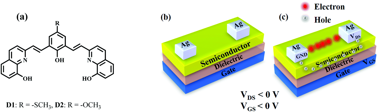 | ||
| Scheme 1 (a) Chemical structure of the organic semiconducting materials D1 and D2; (b) cross-section of OFETs based on D1 and D2 as the organic semiconductor layers in Bottom-Gate-Top-Contact structures: Ag(S&D)/D1 or D2/PMMA/ITO; (c) at negative applied voltage, the accumulation of holes occurs for active transistor action. | ||
Results and discussion
The π-conjugated oligomeric compounds, D1 and D2, were synthesized by reacting 8-hydroxyquinaldine with the corresponding dialdehydes in acetic anhydride under reflux conditions following a reported procedure.19D1 and D2 showed solubility in tetrahydrofuran (THF) and a few aprotic solvents.Single crystals of D1 suitable for crystallographic analyses were grown from methanol by the dichloromethane diffusion method. The crystals of D2 grown under similar conditions were poorly diffracting and our repeated attempts to grow good quality crystals were unsuccessful. D1 crystallized in monoclinic P21/c space group having one molecule and one solvent water molecule in the asymmetric unit. The structure and refinement data of D1 are given in Table S1 in the ESI† and the molecular structure showing atom labeling scheme is given in Fig. 1.
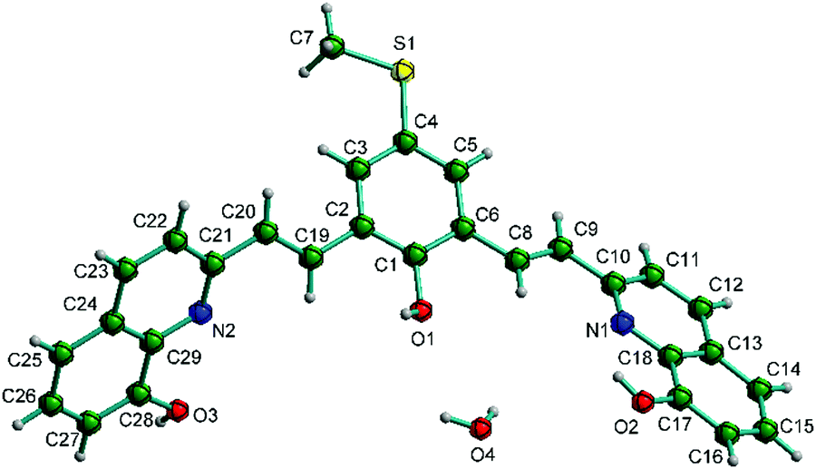 | ||
| Fig. 1 Molecular structure of D1 showing atom labeling scheme. | ||
The molecule shows E conformation about both the styryl C![[double bond, length as m-dash]](https://www.rsc.org/images/entities/char_e001.gif) C bonds. The plane of the 8-HQ ring consisting of the atoms C10–C18 and N1 makes a dihedral angle of 31.23° with the plane of the central phenol ring (consisting of atoms C1–C6), while the second 8-HQ ring consisting of atoms C21–C29 and N2 makes a dihedral angle of 54.31° with the plane of the central phenol ring. This shows that the molecule is not planar and exhibits a twisted geometry, see Fig. 2. This contrasts with the similar compounds reported by Liang et al.,17 in which the two quinolyl rings were more or less coplanar with the central aromatic ring. The bond distances C8–C9 and C19–C20 of the styryl moieties are 1.327(6) and 1.349(6) Å respectively, which are characteristic of the double bonds of alkenyl groups. The C6–C8, C9–C10, C2–C19 and C20–C21 bond lengths are 1.463(6), 1.478(6), 1.474(5) and 1.476(5) Å, respectively, which are slightly shorter than the standard C–C single bond length (ca. 1.5 Å) probably due to conjugation.
C bonds. The plane of the 8-HQ ring consisting of the atoms C10–C18 and N1 makes a dihedral angle of 31.23° with the plane of the central phenol ring (consisting of atoms C1–C6), while the second 8-HQ ring consisting of atoms C21–C29 and N2 makes a dihedral angle of 54.31° with the plane of the central phenol ring. This shows that the molecule is not planar and exhibits a twisted geometry, see Fig. 2. This contrasts with the similar compounds reported by Liang et al.,17 in which the two quinolyl rings were more or less coplanar with the central aromatic ring. The bond distances C8–C9 and C19–C20 of the styryl moieties are 1.327(6) and 1.349(6) Å respectively, which are characteristic of the double bonds of alkenyl groups. The C6–C8, C9–C10, C2–C19 and C20–C21 bond lengths are 1.463(6), 1.478(6), 1.474(5) and 1.476(5) Å, respectively, which are slightly shorter than the standard C–C single bond length (ca. 1.5 Å) probably due to conjugation.
 | ||
| Fig. 2 Figure showing the face-to-face π–π stacking interactions (red dotted lines) among the adjacent molecules of D1 in solid-state. | ||
The two 8-HQ moieties of each molecule of D1 make strong face-to-face π–π stacking interaction with similar moieties of the adjacent molecules as shown in Fig. 2. The π–π stacking interactions are shown as red dotted lines in the figure. Each quinoline ring undergoes π–π stacking interactions with the quinoline rings of adjacent molecules on either side leading to infinite 1-D chain-like arrangements in the crystal lattice, see Fig. 2. In these interactions, the pyridine ring of the 8-HQ moiety is on top of the phenyl ring of the second 8-HQ moiety. The perpendicular distance between the rings varied between 3.491–3.5262 Å, with several C–C distances ∼3.6 Å. The rings are almost parallel (the dihedral angles between the planes vary in the range 1.7–1.77°) in an offset arrangement with slip angles β/γ (formed by the centroid–centroid vector and the ring normal) in the range 18.8–20.4°. The details of these interactions are given in Scheme S1 and Table S2, ESI.†
In addition to the π–π stacking interactions, the crystal structure of D1 also exhibits several H-bonding and other weak bonding interactions as listed in Table 1. The solvent water molecule present in the crystal lattice also undergoes extensive H-bonding interactions. Some of these interactions such as O2–H2⋯O1, O3–H3⋯O4, O1–H1⋯O3, C20–H20⋯S1, C22–H22⋯S1, C12–H12⋯S1, C19–H19⋯O3, C7–H7c⋯S1, O4–H4a⋯O3 and O4–H4b⋯O2 further support and strengthen the 1-D chain-like arrangement along the crystallographic b axis as shown in Fig. S1 in the ESI.† Each of the 1-D chains is further connected to a similar 1-D chain through multiple C27–H27⋯O2 interactions in a centrosymmetric fashion as shown in Fig. S2 and S3, ESI.† The existence of strong face-to-face π–π stacking and other intermolecular interactions in the crystal lattice of D1 points towards its potential charge transport properties as reported earlier.12,13
| D–H⋯A | D–H (Å) | H⋯A (Å) | D⋯A (Å) | D–H⋯A (°) |
|---|---|---|---|---|
| Symmetry codes: 1+X, −1 + Y, +Z; 2+X, 2 + Y, +Z; 31 − X, 1/2 + Y, 1/2 − Z; 42 − X, 1 − Y, 1 − Z; 51 − X, −Y, 1 − Z; 6 +X, 1 + Y, +Z. | ||||
| O2–H2⋯O11 | 0.8200 | 2.27(6) | 2.843(5) | 127(6) |
| O3–H3⋯O42 | 0.8200 | 1.783(6) | 2.602(6) | 175.7(11) |
| O1–H1⋯O31 | 0.8200 | 2.40(3) | 2.913(4) | 121(3) |
| C20–H20⋯S13 | 0.9300 | 3.086(4) | 3.913(4) | 149.12(7) |
| C27–H27⋯O24 | 0.9300 | 2.749(6) | 3.644(6) | 161.94(12) |
| C22–H22⋯S13 | 0.9300 | 3.212(4) | 3.921(4) | 134.56(8) |
| C12–H12⋯S15 | 0.9300 | 3.011(5) | 3.662(5) | 128.41(9) |
| C19–H19⋯O31 | 0.9300 | 2.986(5) | 3.727(5) | 137.72(10) |
| C7–H7c⋯S16 | 0.9600 | 2.95(2) | 3.756(5) | 142(3) |
| O4–H4a⋯O31 | 0.8500 | 2.08(3) | 2.911(6) | 166(10) |
| O4–H4b⋯O26 | 0.8500 | 2.31(8) | 2.962(6) | 133(9) |
Hirshfeld surface analyses
To get quantitative and visual information about the intermolecular interactions, we calculated the Hirshfeld surfaces and the corresponding 2D-fingerprint plots for D1 based on the single-crystal X-ray diffraction data, see Fig. 3 and 4.20,21Fig. 3 shows the Hirshfeld surfaces of D1 displaying shape index and curvedness. Of these, the curvedness maps are particularly useful for identifying planar stacking arrangements.21 Relatively large green flat regions on such surfaces indicate the possibility of stacking interactions. At the same time, the shape index surface represents fine changes in the surface shape, especially in the regions with low curvature, and highlights the regions where the two molecular Hirshfeld surfaces touch each other. The shape index mapping uses red and blue color schemes for complementary pairs of hollows and bumps. Here, the areas on the Hirshfeld surfaces that are simultaneously flat green on the curvedness map and are patterned with red and blue triangles touching each other on the shape index map are of particular importance. Such patterns, often called ‘bow-tie’ patterns, are characteristic of π–π stacking interactions between adjacent molecules.22 In Fig. 3(b), one can observe such features at the flat portions of the surfaces, indicating the existence of π–π stacking interactions. | ||
| Fig. 3 Hirshfeld surfaces of D1 mapped with (a) shape index and (b) curvedness. | ||
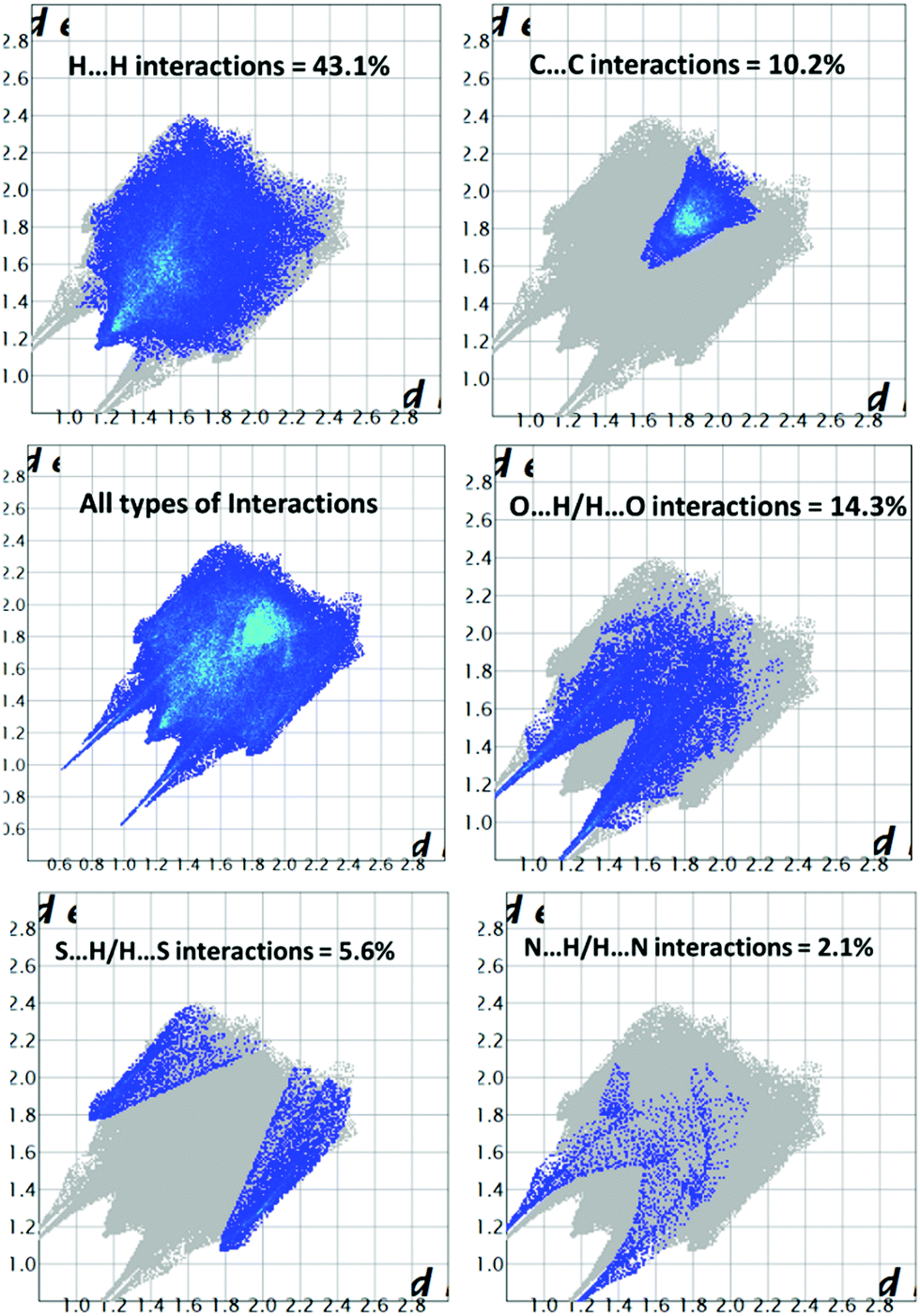 | ||
| Fig. 4 2D fingerprint plots for D1. | ||
The 2D fingerprint plots of D1 are given in Fig. 4. These plots give the percentage contribution of each contact to the total Hirshfeld surface area. As follows from these figures, the major contribution to the total Hirshfeld surface area comes from H⋯H, O⋯H and C⋯C contacts. The 10% contribution by the C⋯C contacts is substantial and further highlights the existence of π–π stacking interactions in the crystal structure. The Hirshfeld surface analyses, therefore, confirm the existence of π–π stacking interactions in the crystal structure of D1.
Optical and electrochemical properties
The optical and electrochemical properties of D1 and D2 were studied by UV-Vis absorption spectra and cyclic voltammetric analyses and the data are given in Table 2. The electronic spectra of D1 and D2 showed strong absorption at 402 and 398 nm respectively in tetrahydrofuran (THF) solutions (Fig. 5) and the corresponding onset absorptions were 460 and 455 nm, respectively. The optical bandgaps of D1 and D2 were estimated as 2.69 eV and 2.72 eV respectively, which further indicated their potential applicability as semiconducting materials.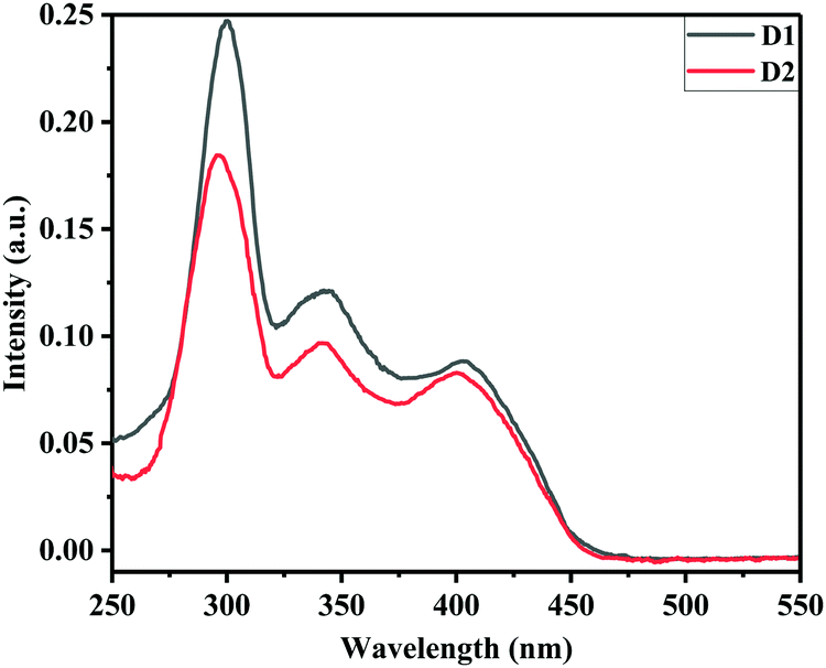 | ||
| Fig. 5 Absorption spectra of D1 and D2 (5 μM) in THF solutions. | ||
The cyclic voltammograms of D1 and D2 are given in Fig. S4 (ESI†). Both D1 and D2 exhibited quasi-reversible oxidation waves at 0.72 V and 0.61 V (E1/2ox., vs. Fc/Fc+) with the corresponding onset oxidation potentials (Eonsetox., vs. Fc/Fc+) of 0.55 V and 0.38 V, respectively. The HOMO energies of D1 and D2 were estimated as −4.90 eV and −4.73 eV and the corresponding LUMO energies as −2.22 eV and −2.00 eV, respectively.23 The HOMO energy levels exhibited by D1 and D2 match with the work function of silver and hence facilitate hole injection. The thermogravimetric analysis of D1 and D2 (see Fig. S5, ESI†) revealed their thermal stability up to 250 °C.
Performance analysis of D1 and D2 as organic semiconductors for OFET application
The semiconducting action of D1 and D2 was investigated by fabricating bottom-gated and top source (S)/drain (D) contact OFET structures on indium-tin-oxide (ITO) coated glass slides (Fig. 6(a)) using cost-effective spin coating technique. The ITO-coated glass slides were cleaned using hot acetone followed by isopropanol (IPA) rinsing. Thereafter, a polymethylmethacrylate (PMMA, ∼120 nm) layer was spin-coated under a controlled nitrogen environment followed by annealing at 120 °C to serve as the dielectric/insulating layer in the OFET structures as shown in Fig. 6(b). Afterward, a ∼250 nm thick active semiconducting layer was deposited by spin-coating the formulated D1/D2 solutions (5 × 10⁻³ M in 10 ml THF; filtered with a 0.2 μm filter) at 3000 rpm (acceleration of 1500 rpm), followed by annealing at 90 °C for 15 min as shown in Fig. 6(c). OFET's source (S) and drain (D) contacts were patterned by thermal deposition of Ag through a standard shadow mask with a channel length (L) of 100 μm and channel width (W) of ∼1 mm as shown in Fig. 6(d). The electrical characteristics of the fabricated Ag/D1/PMMA/ITO and Ag/D2/PMMA/ITO OFET structures were analysed by using a Keithley 4200 SCS characterisation system. | ||
| Fig. 6 Process followed for the fabrication of Ag/D1/PMMA/ITO and Ag/D2/PMMA/ITO OFET structures. | ||
Fig. 7(a) and (b) depict the output and transfer characteristics of the fabricated Ag/D1/PMMA/ITO OFET structure at 75 °C. Similarly, Fig. 7(c) and (d) depict the output and transfer characteristics of the Ag/D2/PMMA/ITO OFET structures at the elevated temperature of 75 °C. It can be seen from Fig. 7(a) and (c) that, at a fixed negative gate to source voltage (Vgs), the drain (D) to source (S) current (Ids) increases with increasing drain to source voltage (Vds) in the negative polarity.
 | ||
| Fig. 7 Electrical characteristics of the Ag/D1/PMMA/ITO and Ag/D2/PMMA/ITO OFETs on glass substrate at 75 °C; (a) output characteristics of Ag/D1/PMMA/ITO, where Vds was swept from 0 to −6 V at Vgs varied from 6 to −6 V with the step of 3 V; (b) Idsvs. Vgs (logarithmic and linear scale) at Vds = −6 V for gate voltage varying from −5 V to 0 V for Ag/D1/PMMA/ITO; (c) output characteristics of Ag/D2/PMMA/ITO, where Vds was swept from 0 to −6 V at Vgs varied from 6 to −6 V with the step of 3 V; (d) Idsvs. Vgs (logarithmic and linear scale) at Vds = −6 V for gate voltage varying from −5 V to 0 V for Ag/D2/PMMA/ITO. | ||
Since, a negative gate bias induces the accumulation of hole carriers at the interface of semiconductor and dielectric layer, the designed and developed D1 and D2 formulations exhibit p-type semiconducting characteristics, and Ag/D1/PMMA/ITO and Ag/D2/PMMA/ITO OFET structures were realized, thereupon. The transistor action of the fabricated bottom gate OFETs may be described by Scheme 1(c). Since the semiconductor is p-type with the majority charge carriers as holes, the channel region is formed only when the applied gate bias is <0 V as depicted in Scheme 1(c). At the applied negative gate voltage, the holes are attracted towards the interface of the semiconductor to the dielectric. Simultaneously, when the drain bias applied is also negative, i.e. <0 V, the accumulated holes in the channel region start to drift towards the drain (D) electrode. Here, a linear increase in the drain current (Ids) with an increase in the drain voltage (Vds) and a considerable saturation of the drain current as a result of an increase in the applied drain voltage establishes the transistor action of fabricated OFET structures. When the applied gate voltage is positive, i.e. >0 V, it can be seen that the drain current starts to decrease. These characteristics correspond to “normally open” field effect transistor. The depletion-mode FETs are normally on due to the electric field built by the existed electrons in the channel region between the source and the drain. Although these cannot be used in switching applications, this type of transistors finds their applications in discrete circuits and as startup circuits to provide some small current during the circuit's power-up sequence and to be shut-off when it is finished.24
When the p-type device operates in the saturation region, the standard equation is modulated to25
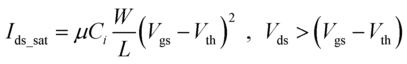 | (1) |
When it operates in the linear region, it is modulated to
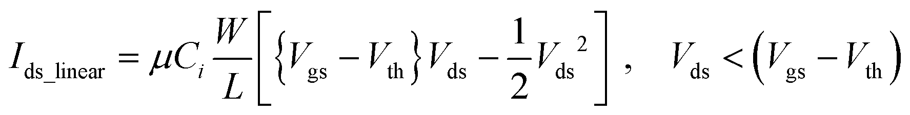 | (2) |
The carrier mobility was extracted from the standard MOSFET equation:26
 | (3) |
The computed hole mobilities of the fabricated Ag/D1/PMMA/ITO and Ag/D2/PMMA/ITO structures were ∼1.28 cm2 V−1 s−1 and ∼1.10 cm2 V−1 s−1 respectively at 75 °C. Parallel thereto, linear extrapolation is a standard threshold voltage (Vth) extraction method from MOSFETs/MISFETs transfer characteristics. Hence, the extracted threshold voltage is from the transfer characteristics (Fig. 7(b) and (d)) of Ag/D1/PMMA/ITO and Ag/D2/PMMA/ITO structures and are assessed to be around −1.55 V and −1.54 V respectively. As listed in Table 3, it is observed that the hole mobilities of D1 and D2 increase upon increasing the substrate temperature from 25 to 75 °C. In comparison to D2, the D1 based OFET structures exhibited higher mobilities that can reach up to ∼1.28 cm2 V−1 s−1 with Ion/off ratio up to 103 at 75 °C; whereas the maximum hole mobility shown by the thin films of D2 was only up to ∼1.10 cm2 V−1 s−1 (see Table 3).
| Temp. (sub.) [°C] | I on/Ioff | V th [V] | μ [cm2 V−1 s−1] | |
|---|---|---|---|---|
| D1 | 25 | 9.71 × 10⁶ | −1.73 | 1.08 |
| 50 | 4.37 × 10⁵ | −1.5 | 1.14966 | |
| 75 | 1.77 × 10³ | −1.55 | 1.276803 | |
| D2 | 25 | 5.30 × 10⁵ | −1.25 | 0.716413 |
| 50 | 2.50 × 10⁴ | −1.41 | 0.85717 | |
| 75 | 2.37 × 10⁴ | −1.54 | 1.106391 |
The performance analyses of the OFETs based on D1 and D2 revealed that these semiconducting materials exhibit good hole mobilities at low voltages (<6 V). This could be attributed to the following factors.27 A good organic semiconducting material, in principle, should have a large electron-delocalized π-conjugated system, good intermolecular interactions, and appropriate energy-level structures.28 For higher charge mobility, the lowest unoccupied molecular orbital (LUMO) or the highest occupied molecular orbital (HOMO) of the OFETs should also favour the injection of electrons or holes. It has been noted experimentally that a HOMO level below ∼−5.0 eV and a LUMO level below ∼−3.7 eV are required for stable hole and electron transport, respectively.29–32 As the experimentally calculated HOMO levels of D1 and D2 are ∼−4.90 eV and ∼−4.73 eV, they lead to stable hole injection during OFET operation.
For a given technology, devices are designed with a specific gate capacitance, which is directly proportional to the dielectric constant (εO) and inversely proportional to the thickness of the gate dielectric material (d) as per the expression:33
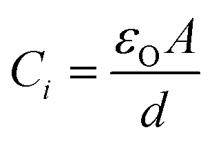 | (4) |
It is clear from the standard MOSFET eqn (2) that the drain current is directly proportional to the capacitance of the dielectric as stated by Michael Salinas et al.33 Therefore, the low voltage operation of the fabricated devices may also be attributed to the higher dielectric constant value of PMMA (4.9)27,34 as compared to SiO2 (3.6). The estimated value of the effective oxide thickness of PMMA is ∼95 nm, which leads to an increase in the effective device capacitance and performance of the investigated OFET structures.
There are a few reports on solution-processable p-type organic semiconductors exhibiting mobilities greater than 1.0 cm2 V−1 s−1; however, many of such devices are reported to work at higher operating voltages.35
Between D1 and D2, the OFETs based on D1 displayed better device performance. The hole mobility exhibited by D1 (1.08 cm2 V−1 s−1) is higher than that of D2 (0.72 cm2 V−1 s−1) at room temperature. This may partly be attributed to the subtle differences in the electronic effects of –R substituent (–SCH3vs. –OCH3) in D1 and D2 as reflected in their respective energy level values, see Table 2. Such subtle changes in the electronic effects of substituents are known to affect the carrier mobilities exhibited by organic semiconductor materials.36–38 To fully understand and compare the effects of different –R groups in determining the charge transport properties, we had also attempted studies using similar compounds having different –R groups. However, those studies were unsuccessful largely due to the poor quality of the thin films obtained from such derivatives. Atomic Force Microscopy (AFM) and X-ray diffraction analyses were performed on thin films as well as powders of D1 and D2 to further explore the reasons behind the differences in their charge mobilities. Fig. 8 depicts the morphologies of the spin-coated thin films of D1 and D2 grown on SiO2/Si as investigated using AFM. Both D1 and D2 exhibited large grains without significant crystalline features with an RMS surface roughness of 6.44 and 2.99 nm respectively for a 5.0 μm × 5.0 μm scan area. D1 and D2 exhibited ball-shaped small grains with a surface roughness of 0.26 and 0.36 nm range respectively for 1.0 μm × 1.0 μm scan area. Overall, Fig. 8 demonstrates that the films based on D1 and D2 exhibit good continuity and flatness required for semiconducting applications. The thin films of D1 exhibited higher mobility which may partly be attributed to the better crystalline nature of D1 as compared to D2. The better crystallinity of D1 is also evident from the XRD data. The powder XRD data of D1 exhibited relatively sharp peaks, while D2 gave comparatively broader peaks showing poor crystalline nature. Both D1 and D2 retained this behaviour in thin films as well, see Fig. S9, ESI.† It has been noted earlier that the mobility increases when the processing induces a more extended crystallization.39,40 This agrees with the fact that the thin films of D2 possess relatively low hole mobility compared to D1.
 | ||
| Fig. 8 Surface morphology of as deposited thin-films of D1 and D2 on Si substrates. | ||
Conclusion
In this work, we have presented two π-conjugated oligomers, 2,2′-(arylenedivinylene)bis-8-hydroxyquinolines D1 and D2, bearing two vinylene-8-HQ units structured around a phenol ring. The structural, electrochemical, optical and semiconducting properties of these oligomers have been investigated. Solution-processed bottom-gate-top-contact OFET devices were fabricated using D1 and D2, which revealed p-type semiconducting behaviours. The OFET structures of D1 and D2 exhibited good device performances with maximum hole mobilities of 1.28 cm2 V−1 s−1 and current on–off ratios of 103 at an operating voltage below 6 V in the case of D1. Single crystal X-ray crystallography and Hirshfeld surface analyses of D1 revealed a dense crystal packing with strong π–π stacking interactions among the molecules leading to infinite 1-D chain-like arrangement in the crystal lattice. The molecules are arranged in a slipped face-to-face manner with perpendicular distance between the rings varying in the range 3.491–3.5262 Å and slip angle of 18.8–20.4°. The excellent π–π stacking interactions contribute to the excellent semiconductor behaviours exhibited by this class of compounds. Even though the styryl-8-HQ derivatives are highly explored for biological and optical applications, their use as organic semiconductors is rarely documented. The present study demonstrates 2,2′-(arylenedivinylene)bis-8-hydroxyquinolines as promising solution-processable organic semiconducting materials holding potential for application in emerging electronics applications. However, more correlation studies connecting the structural and supramolecular properties of this class of compounds with their semiconducting properties are required to fully establish them as promising materials with high charge mobilities. Currently we are engaged in the development and analyses of more such examples.Experimental section
Materials and characterization techniques
PMMA 950 A1 was obtained from Microchem, other chemicals were purchased from Sigma Aldrich. All the solvents were of spectroscopic grade and were used without further treatment. The compounds D1 and D2 were synthesized and characterized following a previously reported procedure.19Single crystal X-ray diffraction analysis
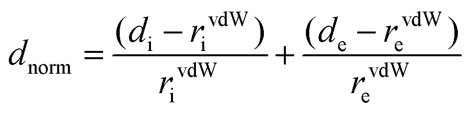
Single-crystal X-ray data were collected on an Agilent SuperNova diffractometer, equipped with a multilayer optics monochromated dual source (Cu and Mo) and an Eos CCD detector, using Cu-Ka radiation (1.54184 Å) at room temperature. Data acquisition, reduction and absorption correction were performed by using CrysAlisPRO.41 The structure was solved with the ShelXS42 program using direct methods and refined on F2 by full-matrix least-squares techniques with ShelXL42 through the Olex2 (v.1.2) program package.43 Due to the poor diffracting properties of the crystal, the quality of the collected data was not very good. Because of the poor-quality data, some of the non-hydrogen atoms had to be refined isotropically. The hydrogen atoms were placed in calculated positions and refined as riding atoms using isotropic displacement parameters. The crystal and structure refinement data are summarized in Table S1, ESI.† There were a few A and B level crystallographic alerts in the Checkcif. These alerts and our explanations for the same are given in ESI.† CCDC 2065427.For a better understanding and quantification of the intra- and intermolecular interactions present in the crystal structure of D1, Hirshfeld surface analyses were performed using the Crystal explorer 17.5 program.44 The Hirshfeld surfaces were drawn from the.cif files of the compounds, with a normalized contact distance (dnorm), which can be expressed as a combination of internal di, external de and van der Waals (vdW) radii of the atoms as below:22,45
Cyclic voltammograms were measured on a computer-controlled Autolab Electrochemical Workstation (Metrohm) instrument at room temperature; the measurements were performed in a conventional three-electrode cell using Pt as the working and counter electrodes, Ag/AgCl (saturated KCl) reference electrode, and n-Bu4NPF6 (0.1 M) as the supporting electrolyte at a scan rate of 50 mV s−1. To calibrate the redox potentials, the cyclic voltammogram of ferrocene was measured under the same conditions. TGA-DTA measurements from room temperature to 500 °C were carried out on a Shimadzu DTG-60 instrument under dry nitrogen flow with a heating rate of 5 °C min−1. The surface morphologies of the as-deposited organic semiconductors, as well as the PMMA dielectric, were examined by using atomic force microscopy (AFM; Dimension Icon from Bruker) in tapping mode with a scan rate of ∼0.5 Hz at room temperature. The high aspect ratio TESPA-HAR AFM probe with resonant frequency 320–369 kHz and spring constant (k) of 20–80 N m−1 was used for AFM measurements. The thickness of the films was confirmed using Stylus Profilometer. The output (Ids − Vds) and the transfer characteristics (Ids − Vgs) of the fabricated FETs were measured using Keithley 4200 SCS characterization system.
Author contributions
The overall experimental design and methodology were prepared by Suman Sehlangia and Prof. Chullikkattil P. Pradeep. The materials synthesis, characterization and related manuscript write-up were performed by Suman Sehlangia. The OFET device related experimental works and write-up were performed by Suman Sehlangia and Shivani Sharma under the supervision of Dr Satinder K. Sharma. Prof. Chullikkattil P. Pradeep supervised the overall project.Conflicts of interest
There is no conflict of interest to declare.Acknowledgements
C. P. P. thanks SERB, Govt. of India for financial support (project no. EMR/2016/002334) and AMRC, IIT Mandi for infrastructural facilities. S. S. thanks MHRD, Government of India, for a fellowship. The authors would like to thank C4DFED, IIT Mandi for providing the fabrication and characterization tools.References
- (a) Y. Qin, G. Li, T. Qi and H. Huang, Mater. Chem. Front., 2020, 4, 1554 Search PubMed; (b) K. Müllen and U. Scherf, Organic Light-Emitting Devices: Synthesis, Properties and Applications, Wiley-VCH, 2006 Search PubMed; (c) K. A. Peterson, A. Patterson, A. Vega-Flick, B. Liaob and M. L. Chabinyc, Mater. Chem. Front., 2020, 4, 3632 Search PubMed.
- (a) M. Mas-Torrent and C. Rovira, Chem. Soc. Rev., 2008, 37, 827 Search PubMed; (b) J. W. Ward, Z. A. Lamport and O. D. Jurchescu, ChemPhysChem, 2015, 16, 1118 Search PubMed.
- (a) Y. Huo, H.-L. Zhang and X. Zhan, ACS Energy Lett., 2019, 4, 1241 Search PubMed; (b) Z. Wang, L. Zhu, Z. Shuai and Z. Wei, Macromol. Rapid Commun., 2017, 38, 1700470 Search PubMed.
- A. Mishra, M. K. R. Fischer and P. Bauerle, Angew. Chem., Int. Ed., 2009, 48, 2474–2499 Search PubMed.
- L.-H. Chou, Y. Na, C.-H. Park, M. S. Park, I. Osaka, F. S. Kim and C.-L. Liu, Polymer, 2020, 191, 122208 Search PubMed.
- (a) H. Li, W. Shi, J. Song, H.-J. Jang, J. Dailey, J. Yu and H. E. Katz, Chem. Rev., 2019, 119, 3 Search PubMed; (b) X. Wu, S. Mao, J. Chen and J. Huang, Adv. Mater., 2018, 30, 1705642 Search PubMed; (c) L. Torsi, M. Magliulo, K. Manoli and G. Palazzo, Chem. Soc. Rev., 2013, 42, 8612 Search PubMed.
- (a) Y. Yu, Q. Ma, H. Ling, W. Li, R. Ju, L. Bian, N. Shi, Y. Qian, M. Yi, L. Xie and W. Huang, Adv. Funct. Mater., 2019, 29, 1904602 Search PubMed; (b) C. Di, Y. Liu, G. U. I. Yu and D. Zhu, Acc. Chem. Res., 2009, 42, 1573 Search PubMed; (c) D. J. Gundlach, Nat. Mater., 2007, 6, 173 Search PubMed; (d) Y. Wen, Y. Liu, Y. Guo, G. Yu and W. Hu, Chem. Rev., 2011, 111, 3358 Search PubMed.
- Y.-G. Ha, J. Nanosci. Nanotechnol., 2015, 15, 6617 Search PubMed.
- F. Yin, L. Wang, X. Yang, M. Liu, H. Geng, Y. Liao, Q. Liao and H. Fu, New J. Chem., 2020, 44, 17552 Search PubMed.
- Z.-F. Yao, J.-Y. Wang and J. Pei, Cryst. Growth Des., 2018, 18, 7 Search PubMed.
- M. Mas-Torrent and C. Rovira, Chem. Rev., 2011, 111, 4833 Search PubMed.
- (a) X. C. Li, H. Sirringhaus, F. Garnier, A. B. Holmes, S. C. Moratti, N. Feeder, W. Clegg, S. J. Teat and R. H. Friend, J. Am. Chem. Soc., 1998, 120, 2206 Search PubMed; (b) J. G. Laquindanum, H. E. Katz, A. J. Lovinger and A. Dodabalapur, Adv. Mater., 1997, 9, 36 Search PubMed; (c) A. N. Sokolov, T. Friscic and L. R. MacGillivray, J. Am. Chem. Soc., 2007, 128, 2806 Search PubMed; (d) J. E. Anthony, Angew. Chem., Int. Ed., 2008, 47, 452 Search PubMed; (e) E. Ahmed, A. L. Briseno, Y. Xia and S. A. Jenekhe, J. Am. Chem. Soc., 2008, 130, 1118 Search PubMed.
- V. Coropceanu, J. Cornil, D. A. da Silva Filho, Y. Olivier, R. Silbey and J.-L. Bredas, Chem. Rev., 2007, 107, 926 Search PubMed.
- Y. Song, H. Xu, W. Chen, P. Zhan and X. Liu, Med. Chem. Commun., 2015, 6, 61 Search PubMed.
- M. Albrecht, M. Fiege and O. Osetska, Coord. Chem. Rev., 2008, 252, 812 Search PubMed.
- C. W. Tang and S. A. VanSlyke, Appl. Phys. Lett., 1987, 51, 913 Search PubMed.
- F. Liang, J. Chen, Y. Cheng, L. Wang, D. Ma, X. Jing and F. Wang, J. Mater. Chem., 2003, 13, 1392 Search PubMed.
- H.-P. Zeng, X.-H. OuYang, T.-T. Wang, G.-Z. Yuan, G.-H. Zhang and X. Zhang, Cryst. Growth Des., 2006, 6, 1697 Search PubMed.
- S. Sehlangia, M. Devi, N. Nayak, N. Garg, A. Dhir and C. P. Pradeep, ChemistrySelect, 2020, 5, 5429 Search PubMed.
- M. A. Spackman and P. G. Byrom, Chem. Phys. Lett., 1997, 267, 215 Search PubMed.
- J. J. McKinnon, M. A. Spackman and A. S. Mitchell, Acta Crystallogr., Sect. B: Struct. Sci., 2004, 60, 627 Search PubMed.
- (a) J. McKinnon, M. Spackman and A. Mitchell, Acta Crystallogr., Sect. B: Struct. Sci., 2004, 60, 627 Search PubMed; (b) A. Y. Sosorev, V. A. Trukhanov, D. R. Maslennikov, O. V. Borshchev, R. A. Polyakov, M. S. Skorotetcky, N. M. Surin, M. S. Kazantsev, D. I. Dominskiy, V. A. Tafeenko, S. A. Ponomarenko and D. Y. Paraschuk, ACS Appl. Mater. Interfaces, 2020, 12, 9507 Search PubMed.
- (a) J. Pommerehene, H. Vestweber, W. Guss, R. F. Mahrt, H. Bassler, M. Prorsch and J. Daub, J. Adv. Mater., 1995, 7, 551 Search PubMed; (b) H. Xin, J. Li, C. Ge, X. Yang, T. Xuea and X. Gao, Mater. Chem. Front., 2018, 2, 975 Search PubMed.
- S.-M. Kang and Y. Leblebigi, CMOS Digital Integrated Circuits, New York, 3rd edn, 1998 Search PubMed.
- S. Sharma, R. Khosla, S. Das, H. Shrimali and S. K. Sharma, Org. Electron., 2018, 57, 14 Search PubMed.
- S. Sharma, R. Khosla, S. Das, H. Shrimali and S. K. Sharma, IEEE Trans. Electron Devices, 2019, 66, 3236 Search PubMed.
- (a) A. Y. Amin, A. Khassanov, K. Reuter, T. Meyer-Friedrichsen and M. Halik, J. Am. Chem. Soc., 2012, 134, 16548 Search PubMed; (b) D. Ji, X. Xu, L. Jiang, S. Amirjalayer, L. Jiang, Y. Zhen, Y. Zou, Y. Yao, H. Dong, J. Yu, H. Fuchs and W. Hu, J. Am. Chem. Soc., 2017, 139, 2734 Search PubMed.
- C. Lu, Z. Ji, G. Xu, W. Wang, L. Wang, Z. Han, L. Li and M. Liu, Sci. Bull., 2016, 61, 1081 Search PubMed.
- C. Guo, J. Quinn, B. Sun and Y. Li, Polym. Chem., 2015, 6, 6998 Search PubMed.
- D. M. de Leeuw, M. M. J. Simenon, A. R. Brown and R. E. F. Einerhand, Synth. Met., 1997, 87, 53 Search PubMed.
- B. S. Ong, Y. Wu, P. Liu and S. Gardner, J. Am. Chem. Soc., 2004, 126, 3378 Search PubMed.
- A. Facchetti, Chem. Mater., 2011, 23, 733 Search PubMed.
- M. Salinas, C. M. Jager, A. Y. Amin, P. O. Dral, T. Meyer-Friedrichsen, A. Hirsch, T. Clark and M. Halik, J. Am. Chem. Soc., 2012, 134, 12648 Search PubMed.
- M. S. Tamboli, P. K. Palei, S. S. Patil, M. V. Kulkarni, N. N. Maldar and B. B. Kale, Dalton Trans., 2014, 43, 13232 Search PubMed.
- (a) H. Ju, K. Wang, J. Zhang, H. Geng, Z. Liu, G. Zhang, Y. Zhao and D. Zhang, Chem. Mater., 2017, 29, 3580 Search PubMed; (b) F. Yin, L. Wang, X. Yang, M. Liu, H. Geng, Y. Liao, Q. Liao and H. Fu, New J. Chem., 2020, 44, 17552 Search PubMed; (c) A. Anjali, R. Dheepika, P. M. Imran, N. S. P. Bhuvanesh and S. Nagarajan, ACS Appl. Electron. Mater, 2020, 2, 2651 Search PubMed; (d) T.-R. Chen, Mater. Lett., 2005, 59, 1050 Search PubMed; (e) L. Yang, N. Zhang, Y. Han, Y. Zou, Y. Qiao, D. Chang, Y. Zhao, X. Lu, J. Wu and Y. Liu, Chem. Commun., 2020, 56, 9990 Search PubMed.
- M. R. Niazi, E. Hamzehpoor, P. Ghamari, I. F. Perepichka and D. F. Perepichka, Chem. Commun., 2020, 56, 6432 Search PubMed.
- S. J. Cho, M. J. Kim, Z. Wu, J. H. Son, S. Y. Jeong, S. Lee, J. Ho Cho and H. Y. Woo, ACS Appl. Mater. Interfaces, 2020, 12, 41842 Search PubMed.
- C.-H. Kuo, D.-C. Huang, W.-T. Peng, K. Goto, I. Chao and Y.-T. Tao, J. Mater. Chem. C, 2014, 2, 3928 Search PubMed.
- (a) C. H. Woo, C. Piliego, T. W. Holcombe, M. F. Toney and J. M. J. Frechet, Macromolecules, 2012, 45, 3057 Search PubMed; (b) J. F. Chang, B. Q. Sun, D. W. Breiby, M. M. Nielsen, T. I. Solling, M. Giles, I. McCulloch and H. Sirringhaus, Chem. Mater., 2004, 16, 4772 Search PubMed.
- R. D. Pietro, T. Erdmann, J. H. Carpenter, N. Wang, R. R. Shivhare, P. Formanek, C. Heintze, B. Voit, D. Neher, H. Ade and A. Kiriy, Chem. Mater., 2017, 29, 10220 Search PubMed.
- CrysAlisPro Program, version 171.37.33c, Agilent Technologies, Oxford, UK, 2012.
- G. M. Sheldrick, Acta Crystallogr., Sect. A: Found. Crystallogr., 2008, 64, 112 Search PubMed.
- O. V. Dolomanov, L. J. Bourhis, R. J. Gildea, J. A. K. Howard and H. J. Puschmann, J. Appl. Crystallogr., 2009, 42, 339 Search PubMed.
- M. A. Spackman and J. J. McKinnon, CrystEngComm, 2002, 4, 378 Search PubMed.
- B. Kupcewicz and M. Malecka, Cryst. Growth Des., 2015, 15, 3893 Search PubMed.
Footnote |
| † Electronic supplementary information (ESI) available. CCDC 2065427. For ESI and crystallographic data in CIF or other electronic format see DOI: 10.1039/d1ma00215e |
| This journal is © The Royal Society of Chemistry 2021 |