 Open Access Article
Influence of A site cation on nonlinear band gap dependence of 2D Ruddlesden–Popper A2Pb1−xSnxI4 perovskites†
Cameron C. L.
Underwood
 ,
J. David
Carey
 and
S. Ravi P.
Silva
 *
*
Advanced Technology Institute, Department of Electrical, Electronic Engineering, University of Surrey, Guildford GU2 7XH, UK. E-mail: s.silva@surrey.ac.uk
First published on 9th July 2021
Abstract
Ruddlesden–Popper phase (RPP) perovskites of the form A1n−1A22BnX3n+1 show great promise in stable photovoltaic (PV) devices or as light emitting diodes (LEDs). In particular, n = 1, monolayer RPPs of the form A2BX4 have also shown great progress as the passivating layer for 3D perovskite PVs. We study the electronic behaviour of mixed B site A2Pb1−xSnxI4 where A = PEA or MA to investigate if the size of the A site cation indirectly affects the nonlinear band gap dependence of a 2D monolayer RPP layer. Both perovskites show a nonlinear behaviour primarily due to the relative energy difference between the Sn 5s–I 5p antibonding states and the Pb 6s–I 5p antibonding states, though the extent of the nonlinearity is reduced relative to 3D bulk perovskites due to the reduced dimensionality of these 2D structures. We also discuss the influence on band gap nonlinearity due to the structural distortions induced by the differences between the A site cation. This research presents a strategy to the design of mixed solid state 2D perovskites by tuning the structural parameters as well as metal and halide composition.
1 Introduction
Halide perovskites have shown great promise for photovoltaic devices within the past decade, with efficiencies rising from 2.8% in their inception in 20091 to 25.5%.2 Due to the remarkable properties of these materials, such as extremely high absorption coefficients, the devices can be very thin and solution processed, leading to a very low cost alternative to currently available technologies, or as an option to integrate perovskites into existing systems, such as silicon–perovskite tandem cells,3–5 but at the current stages are still somewhat limited by stability and the small size of devices.6,7 The majority of research to date has focused on 3D perovskites of the form ABX3, where A = CH3NH3 (methylammonium (MA)), CH2(NH2)2 (formamidinium (FA)) or Cs, with B = Pb or Sn and X = I, Br or Cl.8–12 The majority of success is generally found in materials where some or all of the sites are mixed, such as the triple cation system,13 as this combines the strong properties of each system, while suppressing each systems weaknesses.Replacing Pb as the B site is also very important, as Pb is toxic and water soluble. Sn is a less toxic and much more environmentally friendly alternative,14 which has shown good promise due to the similar chemical properties of Sn compared to Pb. The ionic radius of Sn2+ for a coordination number of 6, as found in perovskites is 1.04 Å, compared to 1.19 Å in the case of Pb2+ so is a favourable substitution.15 Tin based perovskites are generally more unstable in experimental conditions, mostly due to a lower oxidation threshold in Sn2+ to Sn4+, leading to decomposition of the perovskite.16 Mixed Pb–Sn perovskites have been shown to perform well, with a good combination of power conversion efficiencies and much higher stability than pure Sn systems.17 They also have a large range for band gap tuning, giving a particular promise for low band gap materials due to the pronounced band gap bowing observed in these materials.12,18
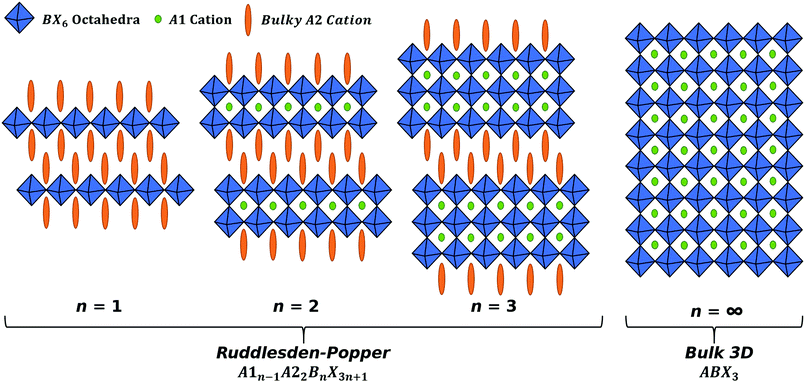
A method to improve on the stability for perovskites is to reduce the dimensionality of the system. Ruddlesden–Popper phase (RPP) perovskites have the general form A1n−1A22BnX3n+1 where n is the number of BX6 octahedra layers between each layer of organic cations,19–21 this is shown in Fig. 1. When n = 1, the RPP perovskite becomes 2D and the simplified form of A2BX4 can be used to describe the material system, where A is a spacer cation, and the RPP perovskite has no internal cation, as there is only one octahedral layer. 2D RPP perovskites have an increased band gap relative to 3D perovskites, due to the reduced dimensionality of the system.22–24 2D (n = 1) and quasi-2D (2 ≤ n ≲ 6) RPP perovskites have been used as top-layers in 2D/3D configurations, allowing not only for high efficiencies, but also high stability.25,26
In a 2D RPP perovskite, the inorganic framework (BX4) has a relatively high dielectric constant, for example εr ≈ 6.1 in (C6H5C2H4–NH3)2PbI4, and is surrounded by a spacer cation with a much lower dielectric constant, for example εr ≈ 2.1 in (C6H5C2H4–NH3)2PbI4, this is also consistent for other RPP perovskites.27 This leads to a phenomena called the dielectric confinement effect, leading to the 2D RPP perovskite having a high exciton binding energy of order hundreds of meV, and 320 meV for the example listed above. Different choices of spacer cations and inorganic frameworks can allow for tuning of this binding energy.28 This high binding energy is significantly larger than mean thermal energy at room temperature (26 meV), so causes RPP devices to be excitonic. The high binding energies of RPP perovskites allow for great promise as light emitting diodes (LEDs), allowing for extremely efficient devices.29,30
As 2D RPP perovskites have much larger band gaps than 3D bulk perovskites, the lower band gap given by replacement of Pb with Sn or Ge becomes even more valuable, due to shifting the band gap further into the visible regime, which makes them more effective light harvesters. Sn-based perovskites show low band gaps of 1.83 eV for n = 1 to 1.20 eV for n = ∞ in (BA)2(MA)n−1SnnI3n+1.31 Mixing the B site of a perovskite has been widely used to partially replace lead, with a less toxic metal such as tin or germanium. This replacement has a notable effect on the band gap of the perovskite, which is comprised of a anti-bonding B s–5p valence band maximum, and a conduction band minimum, comprised an anti-bonding B cation s–5p valence band maximum (VBM) and a conduction band minimum (CBM) comprising mostly of B cation p orbitals. Due to the higher 5s level of Sn (−10.1 eV), relative to the 6s level of Pb (−11.6 eV), the VBM energy increases significantly. The conduction band minimum has a relatively shallower increase, due to the higher 5p energy level of Sn (−3.3 eV) relative to the 6p energy level of Pb (−3.1 eV), this causes a decreased band gap with increasing Sn content.32
Li et al. (2020) previously showed that a small inclusion of Sn in PEA2MAn−1PbnI3n+1 increased broadband emission in n = 1 PEA2PbI4 by 23%, which reduced to <1% in n = 3 PEA2MA2Pb3I10.33 This increase in broadband emission is attributed to the structural distortions caused by the Sn defects causing a slight increase in VBM energy. In 3D bulk perovskites Goyal et al. (2018) investigated this effect for a 3D bulk perovskite of the form MAPb1−xSnxI3, finding a nonlinear dependence of band gap on increasing Sn content, which is attributed primarily to the relative energies of Pb and Sn states.18 The bowing parameter, b, describes how nonlinear the band gap dependence is and is given by eqn (1).
| Eg(x) = (1 − x)Eg(x=0) + xEg(x=1) − bx(1 − x) | (1) |
2 Computational details
The structural and electronic properties for MA2Pb1−xSnxI4 and PEA2Pb1−xSnxI4 are calculated from first principles using non-collinear density functional theory (DFT) employing the Perdew–Burke–Ernzerhof (PBE) generalized gradient approximation37 implemented in the Vienna ab initio simulation program (VASP)38–41 and follows the same techniques used in our previous work,22 where calculations with and without spin–orbit coupling (SoC) were shown to not contribute to the band gap bowing significantly.22,42–44 The structural analysis is completed using Atomic Similations Environment (ASE)45 and post-processed using MatPlotLib, SciPy, Numpy and Seaborn.46–49 Band structure plot fitting was performed in Python with the use of SciPy and NumPy. The resulting PDOS calculations are plotted using a Python script, which is available in the ESI.†Initial position inputs for both MA2PbI4 and PEA2PbI4 are taken from Gebhardt et al.50 and is shown for PEA2PbI4 in the ESI,† for a triclinic P1 configuration, which was shown to have the lowest total energy and replicate the electronic properties well. The simplified unit cell makes it an ideal environment for examining the effects of mixing the B site cation. The unit cell of each calculation contains four sites for the B site ion; in this study we will study the permutations of Pb and Sn. The number of permutations can be described by eqn (2), where N is the total number of sites (in this case 4), m is the number of Sn ions used.
 | (2) |
3 Results and discussion
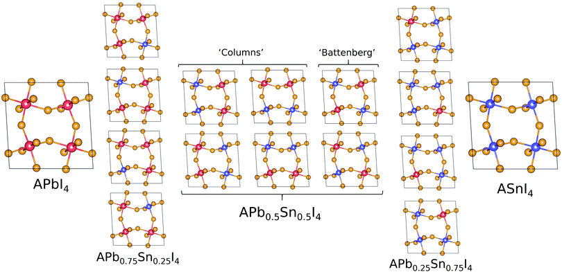
The band gap (eV) as a function of Sn content have been calculated with SoC for MA2Pb1−xSnxI4 and PEA2Pb1−xSnxI4 is shown in Fig. 3 and shows a bowing constant b of 0.40 eV and 0.35 eV, respectively; the band gaps have also been calculated without SoC and show a bowing constant b of 0.43 eV and 0.38 eV, respectively. The difference in band gap and bowing between the two structures can be attributed to the structural distortion induced by each A site cation. There is a significant difference in the calculated band gap of the x = 0.5 compositions between the ‘Columns’ and ‘Battenberg’ permutations, which is due to the decreased dispersion of the ‘Battenberg’ permutation due to the increased mean short range ordering of Pb and Sn pairs, where the ‘Columns’ structures have been previously shown to be slightly lower in energy, possibly suggesting behaviour similar to halide segregation or a preference to forming into ‘Column’ like structures during formation.22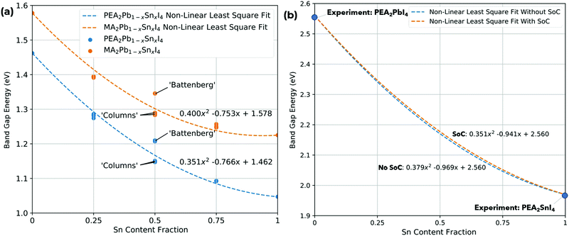 | ||
| Fig. 3 Variation of (a) band gap as a function of Sn content (%) for MA2Pb1−xSnxI4 and PEA2Pb1−xSnxI4 using PBE + SoC. The bowing parameter is 0.400 eV and 0.352 eV, respectively, and (b) band gap as a function of Sn content (%) for PEA2Pb1−xSnxI4 with and without SoC with fixed experimental band gap values for PEA2PbI4 and PEA2SnI4.51–53 | ||
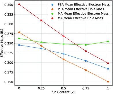 | ||
| Fig. 4 The mean effective electron and hole masses for PEA2Pb1−xSnxI4 and MA2Pb1−xSnxI4 as a function of increasing Sn content. | ||
Whilst the B and X sites directly tune the band edges, the choice of A site cation influences the structural properties of the octahedra, which in turn, indirectly affects the band gap properties of the material. As shown in Fig. 5, in MA2PbxSnxI4, we calculate both larger Pb–I and Sn–I bond lengths relative to PEA2PbxSnxI4, with Pb–I bond angles being consistently larger than Sn–I bond angles by around 0.05 Å due to the relatively smaller ionic radius of Sn relative to Pb. On the other hand in MA2PbxSnxI4, we calculate both a smaller Pb–I–Pb and Sn–I–Sn bond angle relative to PEA2PbxSnxI4. Increasing the B–X bond lengths and B–X–B bond angles result in a lower overlap between the B and X site orbitals, which cause a lower dispersion in the VBM and CBM, increasing the band gap as Sn content increases. The bond angles in PEA2PbxSnxI4 also have a lower variation between permutation, indicating a smaller difference between in-flexed and out-flexed octahedral bond angles. Overall, these B–X–B bond angles, due to the lack of internal A-site cation compared to 3D bulk perovskites, show significant tilting, this, alongside the reduced dimensionality of 2D perovskites, contributes to the high band gaps observed in this class of 2D RPP perovskites.
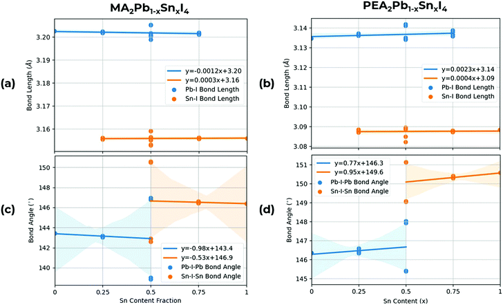 | ||
| Fig. 5 Structural analysis showing mean Pb–I and Sn–I bond lengths for (a) MA2PbxSnxI4, (b) PEA2PbxSnxI422 and mean Pb–I–Pb and Sn–I–Sn bond angles for (c) MA2PbxSnxI4 and (d) PEA2PbxSnxI4.22 A line of best fit is shown with a confidence interval supplied by Seaborn,49 shown by the shaded area. For the Pb–I–Pb and Sn–I–Sn bond angles at x = 0.5, the difference is when the Sn atoms are along the a or b direction, flexing in or out of the unit cell. | ||
All band structure calculations for both MA2Pb1−xSnxI4 and PEA2Pb1−xSnxI4 are direct at the Γ point and show no Rashba splitting, which is consistent with reports for odd layered Ruddlesden–Popper perovskites.50,54 A selection of band structures for each composition of MA2PbI4, MA2SnI4, PEA2PbI4 and PEA2SnI4 with SoC is shown in Fig. 6, and all remaining band structures for all 16 permutations of both MA2Pb1−xSnxI4 and PEA2Pb1−xSnxI4, with and without SoC, are available in the ESI.† The inclusion of SoC is shown decrease the calculated band gap and significantly alter the charge carrier effective masses. Therefore, whilst SoC is not vital in describing the band gap bowing, it is vital for gathering certain accurate electronic properties. The composition of the valence band maximum is shared between Pb 6s–I 5p antibonding or Sn 5s–I 5p respectively, with the conduction band minimum consists of Pb 6p or Sn 5p states, which are shown by the projected colour of the band structure in Fig. 6, with the key given in the top left. This behaviour is consistent with literature for these structures, and does not deviate significantly for different compositions of increasing Sn content.22,23,55
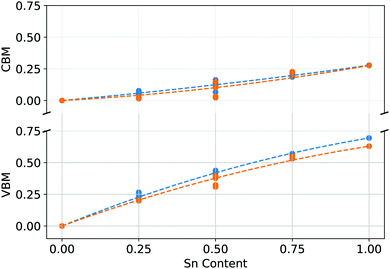 | ||
| Fig. 7 VBM and CBM position as a function of Sn content for (blue) PEA2Pb1−xSnxI4 and (orange) MA2Pb1−xSnxI4. | ||
The mean effective electron and hole masses for PEA2Pb1−xSnxI4 and MA2Pb1−xSnxI4 as a function of increasing Sn content are shown in Fig. 4 are and a full description is shown in the ESI.† There is a decrease in both effective hole and electron masses for PEA2Pb1−xSnxI4 with increasing x. In contrast, the effective electron mass of MA2Pb1−xSnxI4 stays constant while the hole effective mass decreases. There is a decrease in effective electron mass when comparing the use of SoC to without, as shown by the conduction band dispersion of band structures without use of SoC in the ESI,† to a value close to the effective hole mass; this has also been observed for Cs2PbI4 in Liao et al.56 In a mixed Pb–Sn system, balanced electron and hole mobilities are shown for x = 0.5; which could cause longer exciton recombination lifetimes in the active device layer. When not including SoC, the conduction band minimum shows a high effective electron mass going from Γ–Y and a low effective electron mass going from Γ–X or vice versa. Whereas when including SoC, the effective masses are similar along both directions, but vary due to the difference in B–X–B angles caused by the different ionic radius of Pb and Sn. The effective masses can be visually understood by the curvature of the band edges shown in Fig. 6; thus the inclusion of SoC is extremely important for understanding the behaviour of the CBM in PEA2Pb1−xSnxI4 and MA2Pb1−xSnxI4.
The mean distance between pairs of Pb or Sn atoms in both A2Pb0.75Sn0.25I4 and A2Pb0.25Sn0.75I4 is similar for different permutations, but is significantly lower for A2Pb0.5Sn0.5I4 ‘Battenberg’ than A2Pb0.5Sn0.5I4 ‘Columns’. The effect of the short range ordering is most notably observed in PEA2Pb0.5Sn0.5I4 when SoC is not used; as shown in Fig. 3 the band gap varies by over 0.1 eV. In the case where the short range ordered atoms are repeated in the x direction, a CBM band edge is shared by Pb and Sn along the Γ–X direction, and is of Sn character along Y–Γ; this is shown in the ESI.† Whereas in the case that the short range ordered atoms are repeated in the y direction, the CBM band edge is mixed along Y–Γ, with the Sn state occupying slightly lower energies along Γ–X. This is due to the Pb and Sn atoms aligning along either y or x direction for the Y and X points specifically, with either direction having a different B–X–B bond angles, flexing towards the centre of the unit cell and away from the centre. The case of the ‘Battenberg’ structure shows mixed Pb–Sn character on both sides of the CBM, as shown in the ESI,† and has a band gap larger than either ‘Columns’ permutation. As shown in Fig. 6, this behaviour is not observed in the case of using SoC. In terms of characterisation, the inclusion of SoC is a more complete method. This effect is important to consider, as the method of not including SoC is often chosen to study RPP systems as it is much less computationally expensive and gives band gaps closer to experimental data for lower order exchange–correlation functionals. This is due to the cancelling out of the overestimation due to exchange–correlation functional and the band gap decrease given by SoC; this is described in Rappe et al. and Zhao et al.50,54 The lack of dependence of band gap on short range ordering may be due to the increased CBM dispersion when using SoC.
As DFT calculations can miscalculate the band gap of perovskite materials, a method to calibrate the results to experimental data is to fix the boundary conditions for x = 0 and x = 1 in Fig. 3 to the experimental values of PEA2PbI4 = 2.56 eV51,52 and PEA2SnI4 = 1.97 eV.53 This was described in Goyal et al.18 and is shown in Fig. 3(b) for PEA2Pb1−xSnxI4. This also shows that whilst SoC does affect the linear term due to the atomic number (Z) of Pb and Sn. The SoC term scales roughly with Z2, causing a larger band gap difference in PEA2PbI4 compared to PEA2SnI4. Based on these results, SoC is not the root cause of the non-linear term; so a chemical route to non-linearity is studied by analysing the partial density of states.
The band gap (eV) as a function of Sn content (%) for all 16 permutations of PEA2Pb1−xSnxI4, with and without SoC, is shown in the ESI,† showing the difference between PBE and PBE + SoC; inclusion of SoC reduces the band gap in both 2D RPP perovskites, particularly for increased Pb content. We note that the bowing parameter is relatively similar with or without SoC, with MA2Pb1−xSnxI4 being 0.40 eV and 0.43 eV and PEA2Pb1−xSnxI4 being 0.35 eV and 0.38 eV, respectively. The choice of A site has a small effect on the nonlinearity of the system, suggesting the structural behaviour of the octahedra is not the primary source of nonlinearity, but does contribute, which is likely primarily due to the increased B–X in MA2Pb1−xSnxI4, causing an increased band gap, alongside the decreased B–X–B bond angles. This is consistent with results from Goyal et al. (2018)18 for 3D bulk perovskites.
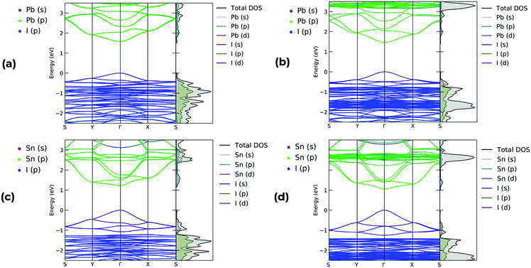
To understand the effect of the relative difference in energies of the Pb and Sn states, we have calculated the PDOS for each structure, with the full dataset shown in the ESI.† In Fig. 8 we show the VBM and CBM composition of (a) MA2Pb0.5Sn0.5I4 ‘Columns’, (b) MA2Pb0.5Sn0.5I4 ‘Battenberg’, (c) PEA2Pb0.5Sn0.5I4 ‘Columns’ and (d) PEA2Pb0.5Sn0.5I4 ‘Battenberg’. In the VBM, there is a notable difference between the relative energies of the Pb and Sn states, which is due to the higher Sn 5s state relative to the Pb 6s atomic energy states, which anti-bond with the I 5p states. Due to the reduced dispersion of the Pb and Sn states, there is an increased band gap in the ‘Battenberg’ permutations relative to the ‘Columns’ permutation, as discussed in Fig. 3.
 | ||
| Fig. 8 Plot of PDOS relative to the calculated Fermi energy highlighting the VBM and CBM composition for (a) MA2Pb0.5Sn0.5I4 ‘Columns’, (b) MA2Pb0.5Sn0.5I4 ‘Battenberg’, (c) PEA2Pb0.5Sn0.5I4 ‘Columns’22 and (d) PEA2Pb0.5Sn0.5I4 ‘Battenberg’.22 The VBM consists mostly of I 5p, Sn 5s and Pb 6s, whereas the CBM consists mostly of Pb 6p and Sn 5p states. The Sn 5s states occupy higher energy than the Pb 6s states in the VBM, contributing to the decrease in band gap. | ||
Analysing the relative position of the VBM and CBM relative to a deep lying reference state is shown in Fig. 7. The VBM increases at a larger rate than the CBM with increasing Sn content, which aligns well to the relative Pb 6s and 6p energy levels to the Sn 5s and 5p levels, as the Pb 6s and Sn 5s states are closer in energy than Pb 6p and Sn 5p. This confirms that the nonlinearity of the band gap is primarily a function of the combination of energy of B site states, which primarily drives a VBM increase, whilst the structural influence of the A site cation is the difference between the two systems, causing a lesser change to the nonlinearity of the band gap as a function of increasing Sn content.
4 Conclusions
The band gap as a function of increasing Sn content in MA2Pb1−xSnxI4 and PEA2Pb1−xSnxI4 was compared using PBE + SoC level DFT calculations and both materials showed a nonlinear band gap dependence with increasing Sn content, with a band gap bowing of 0.400 eV and 0.352 eV respectively. The primary origin of the nonlinearity in both systems is shown to be largely due to the relative energies of the VBM states, due to the higher energy of the Sn 5s states compared to Pb 6s. The difference in nonlinearity between the two systems is attributed to the structural distortions induced by the A site cation, which increase the B–X bond lengths and decrease the B–X–B bond angles in MA2Pb1−xSnxI4 relative to PEA2Pb1−xSnxI4, which cause an increased band gap as well as bowing parameter. The short range ordering of Pb and Sn atoms is also discussed, especially with relation to the use of SoC; the calculated band gap is shown to be dependant on this, due to the increased dispersion of Pb and Sn states in the ‘Columns’ permutations relative to ‘Battenberg’ permutations. This research underlines understanding of mixed solid solution 2D RPP perovskites, and paves the way for improved future compositional engineering, as the combination of the VBM states as well as the structural distortion of the metal-halide octahedras can be varied to tune both the band gap and the bowing parameter, allowing for the opportunity of a low band gap RPP structure for photovoltaic applications or a high band gap RPP structure for blue LED applications.Conflicts of interest
There are no conflicts to declare.Acknowledgements
This work was funded and supported by the Engineering and Physical Sciences Research Council (EPSRC) Grant Number GR/1922310/1 and the MUSICODE EU Horizon Project.Notes and references
- A. Kojima, K. Teshima, Y. Shirai and T. Miyasaka, J. Am. Chem. Soc., 2009, 131, 6050–6051 CrossRef CAS PubMed.
- NREL, Best Research-Cell Efficiencies, 2021.
- Z. Li, Y. Zhao, X. Wang, Y. Sun, Z. Zhao, Y. Li, H. Zhou and Q. Chen, Joule, 2018, 2, 1559–1572 CrossRef CAS.
- F. Sahli, J. Werner, B. A. Kamino, M. Bräuninger, R. Monnard, B. Paviet-Salomon, L. Barraud, L. Ding, J. J. D. Leon and D. Sacchetto, et al. , Nat. Mater., 2018, 17, 820–826 CrossRef CAS PubMed.
- H. H. Park, J. Kim, G. Kim, H. Jung, S. Kim, C. S. Moon, S. J. Lee, S. S. Shin, X. Hao and J. S. Yun, et al. , Small Methods, 2020, 4, 2000074 CrossRef CAS.
- G. Li, K. Chen, Y. Cui, Y. Zhang, Y. Tian, B. Tian, Y. Hao, Y. Wu and H. Zhang, Adv. Opt. Mater., 2020, 8, 1902012 CrossRef CAS.
- A. E. Shalan, Mater. Adv., 2020, 1, 292–309 RSC.
- S. Tao, I. Schmidt, G. Brocks, J. Jiang, I. Tranca, K. Meerholz and S. Olthof, Nat. Commun., 2019, 10, 1–10 CrossRef CAS PubMed.
- C. C. Stoumpos, C. D. Malliakas and M. G. Kanatzidis, Inorg. Chem., 2013, 52, 9019–9038 CrossRef CAS PubMed.
- F. Giustino and H. J. Snaith, ACS Energy Lett., 2016, 1, 1233–1240 CrossRef CAS.
- H. S. Jung and N.-G. Park, Small, 2015, 11, 10–25 CrossRef CAS PubMed.
- F. Hao, C. C. Stoumpos, R. P. Chang and M. G. Kanatzidis, J. Am. Chem. Soc., 2014, 136, 8094–8099 CrossRef CAS PubMed.
- M. Saliba, T. Matsui, J.-Y. Seo, K. Domanski, J.-P. Correa-Baena, M. K. Nazeeruddin, S. M. Zakeeruddin, W. Tress, A. Abate and A. Hagfeldt, et al. , Energy Environ. Sci., 2016, 9, 1989–1997 RSC.
- A. Babayigit, A. Ethirajan, M. Muller and B. Conings, Nat. Mater., 2016, 15, 247–251 CrossRef CAS.
- R. Ouyang, Chem. Mater., 2019, 32, 595–604 CrossRef.
- T. Leijtens, R. Prasanna, A. Gold-Parker, M. F. Toney and M. D. McGehee, ACS Energy Lett., 2017, 2, 2159–2165 CrossRef CAS.
- R. M. I. Bandara, K. D. G. I. Jayawardena, S. O. Adeyemo, S. J. Hinder, J. A. Smith, H. M. Thirimanne, N. C. Wong, F. M. Amin, B. G. Freestone, A. J. Parnell, D. G. Lidzey, H. K. Joyce, R. A. Sporea and S. R. P. Silva, J. Mater. Chem. C, 2019, 7, 8389–8397 RSC.
- A. Goyal, S. McKechnie, D. Pashov, W. Tumas, M. Van Schilfgaarde and V. Stevanovic, Chem. Mater., 2018, 30, 3920–3928 CrossRef CAS.
- S. Ruddlesden and P. Popper, Acta Crystallogr., 1957, 10, 538–539 CrossRef CAS.
- S. Ruddlesden and P. Popper, Acta Crystallogr., 1958, 11, 54–55 CrossRef CAS.
- F. Zhang, H. Lu, J. Tong, J. J. Berry, M. C. Beard and K. Zhu, Energy Environ. Sci., 2020, 13, 1154–1186 RSC.
- C. C. Underwood, J. D. Carey and S. R. P. Silva, J. Phys. Chem. Lett., 2021, 12, 1501–1506 CrossRef CAS PubMed.
- Z. Xiao, Y. Zhou, H. Hosono, T. Kamiya and N. P. Padture, Chem. – Eur. J., 2018, 24, 2305–2316 CrossRef CAS PubMed.
- Z. Xiao, W. Meng, J. Wang, D. B. Mitzi and Y. Yan, Mater. Horiz., 2017, 4, 206–216 RSC.
- G. Grancini, C. Roldán-Carmona, I. Zimmermann, E. Mosconi, X. Lee, D. Martineau, S. Narbey, F. Oswald, F. De Angelis and M. Graetzel, et al. , Nat. Commun., 2017, 8, 1–8 CrossRef.
- Y. Liu, S. Akin, L. Pan, R. Uchida, N. Arora, J. V. Milić, A. Hinderhofer, F. Schreiber, A. R. Uhl and S. M. Zakeeruddin, et al. , Sci. Adv., 2019, 5, eaaw2543 CrossRef CAS.
- K. Gauthron, J. Lauret, L. Doyennette, G. Lanty, A. Al Choueiry, S. Zhang, A. Brehier, L. Largeau, O. Mauguin and J. Bloch, et al. , Opt. Express, 2010, 18, 5912–5919 CrossRef CAS.
- R. K. Misra, B.-E. Cohen, L. Iagher and L. Etgar, ChemSusChem, 2017, 10, 3712–3721 CrossRef CAS PubMed.
- X. Yang, X. Zhang, J. Deng, Z. Chu, Q. Jiang, J. Meng, P. Wang, L. Zhang, Z. Yin and J. You, Nat. Commun., 2018, 9, 1–8 CrossRef.
- H. Tsai, W. Nie, J.-C. Blancon, C. C. Stoumpos, C. M. M. Soe, J. Yoo, J. Crochet, S. Tretiak, J. Even and A. Sadhanala, et al. , Adv. Mater., 2018, 30, 1704217 CrossRef PubMed.
- Y. Chen, Y. Sun, J. Peng, J. Tang, K. Zheng and Z. Liang, Adv. Mater., 2018, 30, 1703487 CrossRef.
- J. Qian, B. Xu and W. Tian, Org. Electron., 2016, 37, 61–73 CrossRef CAS.
- T. Li, X. Chen, X. Wang, H. Lu, Y. Yan, M. C. Beard and D. B. Mitzi, ACS Energy Lett., 2019, 5, 347–352 CrossRef.
- L. Mao, H. Tsai, W. Nie, L. Ma, J. Im, C. C. Stoumpos, C. D. Malliakas, F. Hao, M. R. Wasielewski and A. D. Mohite, et al. , Chem. Mater., 2016, 28, 7781–7792 CrossRef CAS.
- H. Lu, C. Xiao, R. Song, T. Li, A. E. Maughan, A. Levin, R. Brunecky, J. J. Berry, D. B. Mitzi and V. Blum, et al. , J. Am. Chem. Soc., 2020, 142, 13030–13040 CrossRef CAS PubMed.
- P. Cheng, T. Wu, J. Liu, W.-Q. Deng and K. Han, J. Phys. Chem. Lett., 2018, 9, 2518–2522 CrossRef CAS PubMed.
- J. P. Perdew, K. Burke and M. Ernzerhof, Phys. Rev. Lett., 1996, 77, 3865 CrossRef CAS PubMed.
- G. Kresse and J. Hafner, Phys. Rev. B: Condens. Matter Mater. Phys., 1993, 47, 558 CrossRef CAS PubMed.
- G. Kresse and J. Hafner, Phys. Rev. B: Condens. Matter Mater. Phys., 1994, 49, 14251 CrossRef CAS PubMed.
- G. Kresse and J. Furthmüller, Comput. Mater. Sci., 1996, 6, 15 CrossRef CAS.
- G. Kresse and J. Furthmüller, Comput. Mater. Sci., 1996, 54, 11169 CAS.
- A. Togo and I. Tanaka, 2018, arXiv preprint arXiv:1808.01590.
- Y. Hinuma, G. Pizzi, Y. Kumagai, F. Oba and I. Tanaka, Comput. Mater. Sci., 2017, 128, 140–184 CrossRef CAS.
- A. M. Ganose, A. J. Jackson and D. O. Scanlon, J. Open Source Softw., 2018, 3, 717 CrossRef.
- A. H. Larsen, J. J. Mortensen, J. Blomqvist, I. E. Castelli, R. Christensen, M. Dułak, J. Friis, M. N. Groves, B. Hammer, C. Hargus, E. D. Hermes, P. C. Jennings, P. B. Jensen, J. Kermode, J. R. Kitchin, E. L. Kolsbjerg, J. Kubal, K. Kaasbjerg, S. Lysgaard, J. B. Maronsson, T. Maxson, T. Olsen, L. Pastewka, A. Peterson, C. Rostgaard, J. Schiøtz, O. Schütt, M. Strange, K. S. Thygesen, T. Vegge, L. Vilhelmsen, M. Walter, Z. Zeng and K. W. Jacobsen, J. Phys.: Condens. Matter, 2017, 29, 273002 CrossRef PubMed.
- J. D. Hunter, Comput. Sci. Eng., 2007, 9, 90–95 Search PubMed.
- P. Virtanen, R. Gommers, T. E. Oliphant, M. Haberland, T. Reddy, D. Cournapeau, E. Burovski, P. Peterson, W. Weckesser, J. Bright, S. J. van der Walt, M. Brett, J. Wilson, K. J. Millman, N. Mayorov, A. R. J. Nelson, E. Jones, R. Kern, E. Larson, C. J. Carey, İ. Polat, Y. Feng, E. W. Moore, J. Vander Plas, D. Laxalde, J. Perktold, R. Cimrman, I. Henriksen, E. A. Quintero, C. R. Harris, A. M. Archibald, A. H. Ribeiro, F. Pedregosa, P. van Mulbregt and SciPy 1.0 Contributors, Nat. Methods, 2020, 17, 261–272 CrossRef CAS PubMed.
- C. R. Harris, K. J. Millman, S. J. van der Walt, R. Gommers, P. Virtanen, D. Cournapeau, E. Wieser, J. Taylor, S. Berg, N. J. Smith, R. Kern, M. Picus, S. Hoyer, M. H. van Kerkwijk, M. Brett, A. Haldane, J. F. del R'o, M. Wiebe, P. Peterson, P. G'erard-Marchant, K. Sheppard, T. Reddy, W. Weckesser, H. Abbasi, C. Gohlke and T. E. Oliphant, Nature, 2020, 585, 357–362 CrossRef CAS PubMed.
- M. L. Waskom, J. Open Source Softw., 2021, 6(60), 3021 CrossRef.
- J. Gebhardt, Y. Kim and A. M. Rappe, J. Phys. Chem. C, 2017, 121, 6569–6574 CrossRef CAS.
- F. Thouin, D. A. Valverde-Chávez, C. Quarti, D. Cortecchia, I. Bargigia, D. Beljonne, A. Petrozza, C. Silva and A. R. S. Kandada, Nat. Mater., 2019, 18, 349–356 CrossRef CAS PubMed.
- L. Gan, H. He, S. Li, J. Li and Z. Ye, J. Mater. Chem. C, 2016, 4, 10198–10204 RSC.
- L. Lanzetta, J. M. Marin-Beloqui, I. Sanchez-Molina, D. Ding and S. A. Haque, ACS Energy Lett., 2017, 2, 1662–1668 CrossRef CAS.
- Y.-Q. Zhao, Q.-R. Ma, B. Liu, Z.-L. Yu, J. Yang and M.-Q. Cai, Nanoscale, 2018, 10, 8677–8688 RSC.
- Y. Fu, X. Jiang, X. Li, B. Traoré, I. Spanopoulos, C. Katan, J. Even, M. G. Kanatzidis and E. Harel, J. Am. Chem. Soc., 2020, 142, 4008–4021 CrossRef CAS PubMed.
- C.-S. Liao, Q.-Q. Zhao, Y.-Q. Zhao, Z.-L. Yu, H. Zhou, P.-B. He, J.-L. Yang and M.-Q. Cai, J. Phys. Chem. Solids, 2019, 135, 109060 CrossRef CAS.
Footnote |
| † Electronic supplementary information (ESI) available. See DOI: 10.1039/d1ma00491c |
| This journal is © The Royal Society of Chemistry 2021 |

