
 Open Access Article
 This Open Access Article is licensed under a Creative Commons Attribution-Non Commercial 3.0 Unported Licence
Zinc oxide heterostructures: advances in devices from self-powered photodetectors to self-charging supercapacitors
Sukanta
Nandi
 ,
Sumana
Kumar
and
Abha
Misra
*
,
Sumana
Kumar
and
Abha
Misra
*
Department of Instrumentation and Applied Physics, Indian Institute of Science, Bangalore, Karnataka 560012, India. E-mail: abha.misra1@gmail.com
First published on 9th September 2021
Abstract
Over the years, zinc oxide (ZnO) has become a well-studied material due its versatile properties including both wide bandgap and large room temperature excitonic binding energy. The thermally-stable phase of ZnO allows it to grow in various nanostructures with high surface to volume ratio. So far, ZnO-based ultraviolet photodetectors (PD) have been a popular application in various heterostructures (HSs), and its piezoelectric properties have been exploited for the self-powering capability of devices. Both optical and mechanical excitations in combination provide a unique capability for the generation of excitons with built-in potential that has currently developed a vast interest in self-powered PDs as well as the energy storage capability in supercapacitors (SCs). This review provides a comprehensive detail of ZnO-based HSs exploited for interface engineering to provide a zero bias photoresponse and further being utilized for optically-activated SC applications. The self-powered photoresponse in ZnO is achieved through bandgap engineering by combining various semiconducting interfaces for broadband responses, fast response time, flexible devices, etc. Moreover, the ZnO interface along with electroactive materials in SC electrodes not only provides electrochemical routes for charge generation and separation but also the optical response, which is further attributed to self-powered voltage generation for efficient charge separation. The review describes the fundamental structural properties of ZnO along with its optical, electronic, and mechanical properties. The characteristics and significance of HSs in the field of science and technology is discussed in detail with emphasis on ZnO-based HSs. Thereafter, the optical interaction in ZnO-based HS is extended for two prominent applications targeting its self-powering/charging capability, i.e., PDs and SCs. Apart from the optical response, the contribution of mechanical and thermal stimuli toward these self-operating systems is also presented.
Introduction
Zinc oxide (ZnO) is an universally known semiconductor in the field of blue and ultraviolet (UV) optical devices due to its wide bandgap (Eg) and large room temperature (RT) excitonic binding energy.1–3 The crystal structure of ZnO is categorized into zinc blende, wurtzite, and rocksalt, where under ambient conditions, the thermodynamically stable phase is the wurtzite one (ZnO properties are listed in Table 1). Importantly, the ability to grow as a single crystal wurtzite substrate provides ZnO several additional advantages over other semiconductor materials.4,5 The wurtzite crystal structure of ZnO has a hexagonal lattice where Zn ions are surrounded by O ions in a tetrahedral arrangement of alternating planes and due to its crystal structure, it has a mixed ionic and covalent nature.5,6 The tetrahedral coordination in ZnO along the hexagonal axis gives rise to a polar symmetry, which induces spontaneous polarization for piezoelectricity and pyroelectricity. Moreover, polarity along the preferred dimension also plays a deciding role in crystal growth and defect generation.2| Material properties | Material parameters |
|---|---|
| Material type | II–VI compound semiconductor (n-type) |
| Crystal structure and type | Hexagonal, P63mc space group, polar and non-centrosymmetric |
| Zn–O distance along the c-axis | 1.90 Å |
| Zn–O distance along the a-axis | 1.98 Å |
| Lattice parameters | a = 3.249 and c = 5.206 Å |
| Unit cell volume | 47.63 Å3 |
| Density | 5.606 g cm−3 |
| Bandgap | ∼3.37 eV at 300 K, direct |
| Exciton binding energy/diameter | ∼60 meV at ∼300 K/∼2 nm |
| Other associated properties | Piezoelectric, pyroelectric |
Fig. 1 depicts the details of the atomic arrangements in wurtzite ZnO. The faces with Zn at (0001) and O at (000![[1 with combining macron]](https://www.rsc.org/images/entities/char_0031_0304.gif) ) along with (100) have Zn and O atoms in equal number.2Fig. 1(a) and (b) depicts the projections of both [0001] and [111] planes in a three-dimensional view. Fig. 1(c) schematically depicts the hexagonally closed packed sublattices of wurtzite ZnO, where each sublattice consists of both Zn and O atoms along the c-axis.5
) along with (100) have Zn and O atoms in equal number.2Fig. 1(a) and (b) depicts the projections of both [0001] and [111] planes in a three-dimensional view. Fig. 1(c) schematically depicts the hexagonally closed packed sublattices of wurtzite ZnO, where each sublattice consists of both Zn and O atoms along the c-axis.5
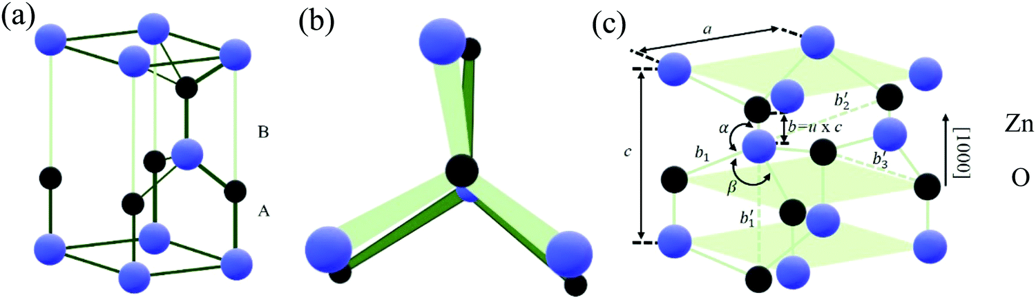 | ||
| Fig. 1 Crystal structure of wurtzite ZnO in a view (a) normal to and (b) along the [0001] and [111] crystallographic planes. (c) Zn and O atom arrangement in the wurtzite ZnO structure with the basal plane and direction shown by the lattice constants a and c, respectively. The bond length is designated by the u parameter.5 [Adapted by permission from John Wiley & Sons: Wiley Books, H. Morkoç and Ü. Özgür, 1–765 © 2009]. | ||
ZnO, with its unique physical and chemical properties, is obtained in various nanostructures (NSs) due to its high chemical stability and a broad chemistry for wet chemical etching. Therefore, these NSs with paramagnetic nature, broad range of radiation absorption, and high electrochemical coupling coefficient have presented a wide platform for electronic and optoelectronic devices, and thus emerged as a key material with the fast development of growth technologies. The next sections further elaborates the ZnO properties associated with its electrical, optical, and piezoelectric characteristics.
Electrical and optical characteristics of zinc oxide
The electrical characteristics of ZnO highly depend on its structure and the doping conditions. Under undoped conditions, ZnO shows n-type behavior with ∼1017 cm−3 donor concentration.2,8 Further, n-type doping may induce the largest carrier concentration of ∼1021 electrons (e−s) cm−3 with e− effective mass of 0.24m0 and Hall mobility of 200 cm2 V−1 s−1. On the other hand, a concentration of ∼1019 holes (h+s) cm−3 is used for p-type doping with h+ effective mass of 0.59 m0 and Hall mobility of 5–50 cm2 V−1 s−1 at RT.2,7,8 The intrinsic n-type conductivity in ZnO has been reported to be introduced via O vacancy or Zn interstitials or through impurity incorporation via the creation of shallow donors such as that of hydrogen (H2).4,9 These native defects or intrinsic defects thus play a significant role in determining both the electrical and optical characteristics of ZnO.4 These defects affect various factors such as doping, optical efficiency, and minority carrier lifetime.4 During ZnO growth or annealing, the native point defects create a situation of oxygen-deficiency, thereby acting as a source of self-compensation upon interaction with external stimuli.4 In case of hydrogenated ZnO, the interstitial electronic transition level of H2 always lies in the conduction band (CB). Thus, the role of H2 is to always act as a donor irrespective of whether ZnO is n or p-type.The optical properties of ZnO are mainly attributed to its large Eg, which is due to the largest ionization energy of O and, thus, a strong interaction between the Zn-3d and O-2p orbitals.3 The doping of ZnO not only controls the carrier concentration for modified mobility but is also widely used for tuning the optical interactions. For example, Lotin et al. have shown that the Eg of ZnO could be tuned from 3.3 to 5.72 eV on alloying with magnesium (Mg) and the same was redshifted to 2.51 eV on cadmium (Cd) alloying.10 Similarly, other studies demonstrated the tuning of the optical Eg of ZnO via doping with 3d transition metal ions (∼2.1–3.5 eV), such as aluminum (Al) (∼3.15–3.20 eV), copper (Cu) (∼3.1–3.18 eV), lithium (Li) (∼3.17–3.26 eV), and nickel (Ni)-tin (Sn) dual doping (∼3.86–4.0 eV). Fig. 2(a)–(d) depicts the Eg variation for varying the concentration of Cd, Mg, Li, Al, and transition metal ions, respectively.11–15
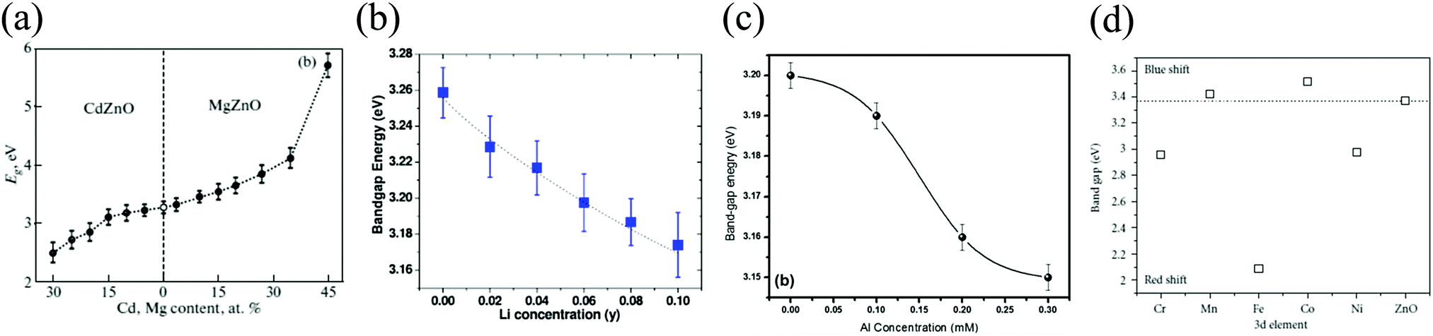 | ||
| Fig. 2 E g energy dependence on the alloying/doping concentration of (a) Cd, Mg, (b) Li, (c) Al, and (d) 3d transition metal ions.10,11,13,15 [Reprinted by permission from Springer Nature: Phys. Solid State, A. A. Lotin et al., 53, 467–471,10 © 2011, American Institute of Physics: J. Appl. Phys., S. U. Awan et al., 116, 083510,11 © 2014, Springer Nature: Appl. Phys. A Mater. Sci. Process., A. Shah et al., 125, 1–8,13 © 2019, and Hindawi: J. At. Mol. Opt. Phys., D.P. Joseph and C. Venkateswaran, 2011, Article ID 270540, 1–715 © 2011]. | ||
High RT excitonic binding energy (∼60 meV) makes ZnO stand out from other UV detecting materials, for e.g., gallium nitride (GaN). Such a high binding energy (∼2.4 times higher than that of GaN) leads to stimulated emission beyond RT, thus making ZnO ideal for light emitting/laser diodes.3,16
Moreover, the photoconductivity of ZnO is greatly influenced by its surface chemistry, with the NSs transport characteristics being affected by depletion layer formation, surface band-bending, and Fermi-level (Ef) pinning.17 An additional surface chemistry can be induced with external stimuli, for e.g., optical illumination. The additional energy for oxygen desorption causes the diffusion of e− and/or h+ to the surface, as depicted schematically in Fig. 3, and thus influences the conductivity of the ZnO NSs-based devices through band bending. Light illumination on ZnO with the above Eg results in the separation of the generated excitons caused by the electric field in the surface region either through external bias or induced biasing (i.e., self-powered; no external applied bias). The photoresponse in ZnO NSs has a much longer decay with the recombination of the excited e−–h+ pairs; thus, the decay time is in the order of seconds, minutes, and hours as opposed to that of other semiconductors.17
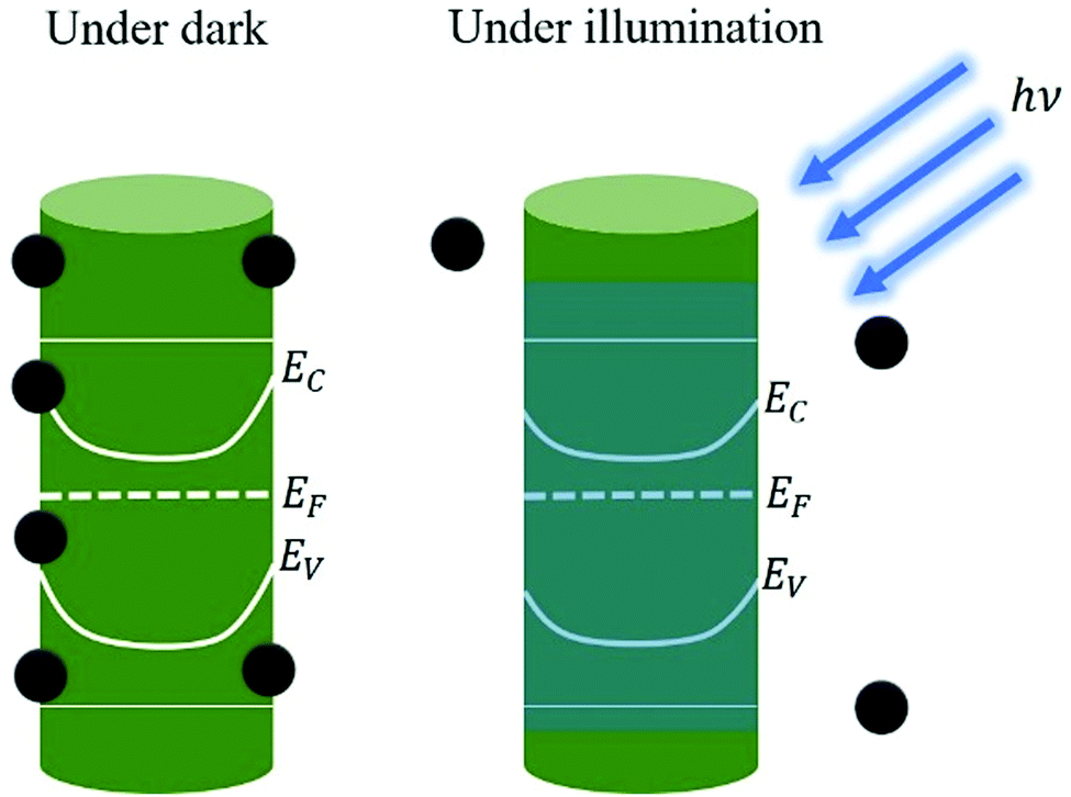 | ||
| Fig. 3 Surface and the desorption of adsorbed oxygen molecules in a ZnO nanorod (NR) upon illumination is shown to have band bending.17,18 [Adapted from ref. 18, Nanotechnology, E. Schlenker et al., 19, 365707,18 https://doi.org/10.1088/0957-4484/19/36/365707, © 2008, with permission from IOP Publishing, Ltd]. | ||
Piezoelectric characteristics
Larger electromechanical coupling in ZnO is attributed to the highest piezoelectric constants than that among the tetrahedrally-bonded semiconductors, for e.g., GaN and AlN;5,19 thus, it is greatly desirable for use in piezotransducers with large electromechanical coupling.As mentioned earlier, wurtzite ZnO has a spontaneous polarization along the c-direction due to its low symmetry. Moreover, in addition to its piezoelectric nature, ZnO also displays a pyroelectric behavior, where the electric displacement gets changed due to thermal expansion arising out of strain. Generally, pyroelectricity is shown by materials having no central symmetry, non-zero dipole moment of their molecular structure, and having either rotational symmetry on a sole axis other than in an inversion axis or no axis of rotational symmetry.5Fig. 4 schematically depicts the correlation between the electrical, mechanical, and thermal energies that lead to the occurrence of primary and secondary pyroelectric effects.
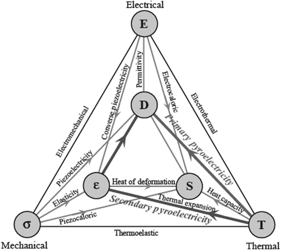 | ||
| Fig. 4 Non-centrosymmetric materials exhibiting a connection between the thermal, mechanical, and electrical energies for piezoelectric and pyroelectric effects.5 [Reprinted by permission from John Wiley & Sons: Wiley Books, H. Morkoç and Ü. Özgür, 1–765 © 2009]. | ||
Introduction to heterostructures and its significance
ZnO has an additional advantage of being synthesized in different forms of nanomaterials,1 zero-dimensional quantum dots (QDs),20,21 one-dimensional nanowires (NWs)/rods,22,23 and two-dimensional flakes (NFs).24 This extra degree of freedom bestows on it the flexibility to form junctions with other materials and form the so-called heterostructures (HSs). An HS is a structure characterized by spatially varying chemical composition. Such a structure is formed when two dissimilar semiconductors/oxides are bonded to one another, forming interfacial junctions and thereby creating a spatial compositional variation.25,26 The advantage of HSs is that they empower us to control the states and the charge carrier motion, for e.g., in a semiconductor.25 This in turn provides ample room to tune the optical, electrical, and optoelectrical properties of the device as a whole.27–32 In addition, the interfacial regions of heterojunctions are regions capable of hosting several novel states, functionalities, and phenomenon, and are thus of immense significance for exploring fundamental physics.33–37 For e.g., Ohtomo et al., and Thiel et al., demonstrated the existence of 2D e− gas at the interface of oxide HSs.38,39 Likewise, various other demonstrations, such as the existence of superconducting interfaces between insulating oxides,40 high temperature interface superconductivity between metallic and insulating oxides,41 and ferroelectricity in perovskite oxide artificial superlattices,42 have been presented over the years.33–37,43,44 Moreover, it is not only the interfacial physics but even the interfacial chemistry that plays a major role in the thermodynamic stability and device performance of mainly two-dimensional devices. A comprehensive review on the interfacial chemistry of two-dimensional HSs can be found in a recent publication by Gbadamasi et al.45 Another important field of research where HSs, in particular semiconductor HSs, have made great impact, is the field of photocatalysis.46 In this field, HSs are employed mainly to overcome two major problems: (1) limited visible-light absorption and (2) quick charge recombination processes or, in other words, low charge separation efficiency.46 Recently, Zhang et al., provided theoretical insights into the photocatalytic mechanism of covalent organic framework C4N and molybdenum disulfide (MoS2) for the CO2 reduction reaction.47 In their study, they found that the HS exhibits a type-II band alignment with improved mobility arising from the reduced effective masses of h+ and e− as compared to their respective counterparts in the C4N and MoS2 monolayer. Furthermore, from the optical properties, they found that the HS depicted a broadband visible light absorption (1.55–3.1 eV) with comparatively higher absorption coefficient than C4N and MoS2. The synergy of these two effects thus enabled C4N/MoS2 HS to be an efficient visible light-harvesting photocatalyst.47 In another photocatalytic application, an HS of g-C3N4/NiTiO3 has proven to be an efficient photocatalyst for water treatment.48 Synthesized with a one-step calcination method, the HS exhibited a larger surface area, strong visible light absorption, and efficient e−–h+ pair separation. The overall effect was that of an efficient nitrobenzene remover with a removal rate of 0.0132 min−1, which was higher by a factor of ∼1.8 and ∼1.6 times as compared to the respective removal rates of g-C3N4 and NiTiO3.48 Likewise, forming an HS of the same g-C3N4 with Mo2C@C helped to tackle the second problem (already mentioned earlier) persistent in photocatalytic devices.49 Mo2C@C, with its exceptional e− capturing capability and superior conductivity, led to the capturing along with the efficient transfer of the photogenerated (visible) e−s, resulting in h+ accumulation. The net result of such HS design was an excellent HS-based photocatalytic system for H2 production.49 Thus, in a nutshell, it has been observed that over the years, the field of HSs has attracted numerous researchers to work and develop them toward modern solid state devices, almost impacting 2/3 of the total semiconductor physics community.21,35,45,46,50–56 HSs have played a vital role toward the development of modern technologies, which otherwise could not have been achievable with a single semiconductor material.31 As an appreciation toward this scientific triumph, the Nobel committee awarded 1/2 the total share of the 2000 Nobel prize in physics to Late Prof. Zhores I. Alferov and Prof. Herbert Kroemer for their outstanding contribution toward developing semiconductor HSs for high-speed electronics and optoelectronics.57Zinc oxide-based heterostructures
The wide availability of various ZnO NSs coupled with their simple, low-cost, and well-established synthetic techniques have resulted in a plethora of ZnO-based HSs, with applications spanning from energy conversion to energy storage devices.30,58–61 Forming a ZnO HS has proved to be an efficient way of improving the performance of a pristine ZnO device with novel functionalities. The main consequences of such HSs are as follows: (1) band alignment (mostly type-I or II), resulting in strong interfacial built-in electric fields. This interfacial field assists in the effective separation of the external stimuli generated charge carriers and also providing self-powering (no applied external field) capabilities to ZnO-based devices.58,62–64 (2) Reduction in the optical bandgap and also the improvement of the optical properties/characteristics.30,65,66 (3) Improving the energy storage capability via synergistic contribution to device electrochemistry.61,66 For e.g., Bhatnagar et al., reported a transparent self-powered (zero external bias) neuromorphic device based on nickel oxide (NiO)/ZnO HS.58 The p–n junction (p-NiO and n-ZnO) generates a built-in electric field and helps in the spontaneous (without external bias) separation of the photogenerated (@400 nm) charge carriers with an open-circuit voltage of 482 mV and a short-circuit current of 838 µA cm−2. In another study, Wang et al., theoretically investigated the effect of HS formation between transition metal dichalcogenides and 2D ZnO on the structural, optical, and electronic properties.63 From their investigation, they found that the HS of ZnO with MoS2 and WS2 resulted in type-II band alignment with strong built-in electric field (Fig. 5(a)), thus providing an ideal configuration for photovoltaic devices. On the other hand, the band alignment with the selenium counterparts, i.e., MoSe2 and WSe2, results in a type-I alignment (Fig. 5(b)), a configuration ideal for optical devices such as LEDs. Moreover, the HSs also exhibited improved optical absorption in the visible and infrared (IR) regions. Fig. 5(c) depicts the optical absorption of C2N/ZnO HS with improved characteristics in the range of 400–760 nm, thereby signifying the effective utilization of sunlight by the HS.65 Furthermore, the type-II band alignment in MoS2/ZnO HS has proved to be an efficient strategy toward improved photocatalysis, for e.g., water splitting.62 Numerous studies in the past have shown that MoS2 is an efficient photocatalytic material for water splitting, degrading pollutants, and photosynthesis.67–70 However, pristine MoS2 faces the problem of high recombination rate (among many other problems) owing to the stagnation of the photogenerated charge carriers in the same spatial regions.62,67 This problem of charge stagnation, and thus efficient separation and collection has been achieved via the formation of an HS with ZnO.62Fig. 5(d) schematically depicts the efficient movement of photogenerated charge carriers (e−s and h+s) at the HS interface.62 This concept of band alignment, when applied to solar cells, results in increased power conversion efficiency.59 A study by Kaphle et al., showed that the intrinsic band alignment in a p–n junction solar cell of p-CuO/n-ZnO (Fig. 5(e)) can be effectively tuned via Co doping.59 The result showed a transition from type-II to type-I band alignment (Fig. 5(f)) along with an enhanced power conversion efficiency of ∼1.87% for 10% Co doping.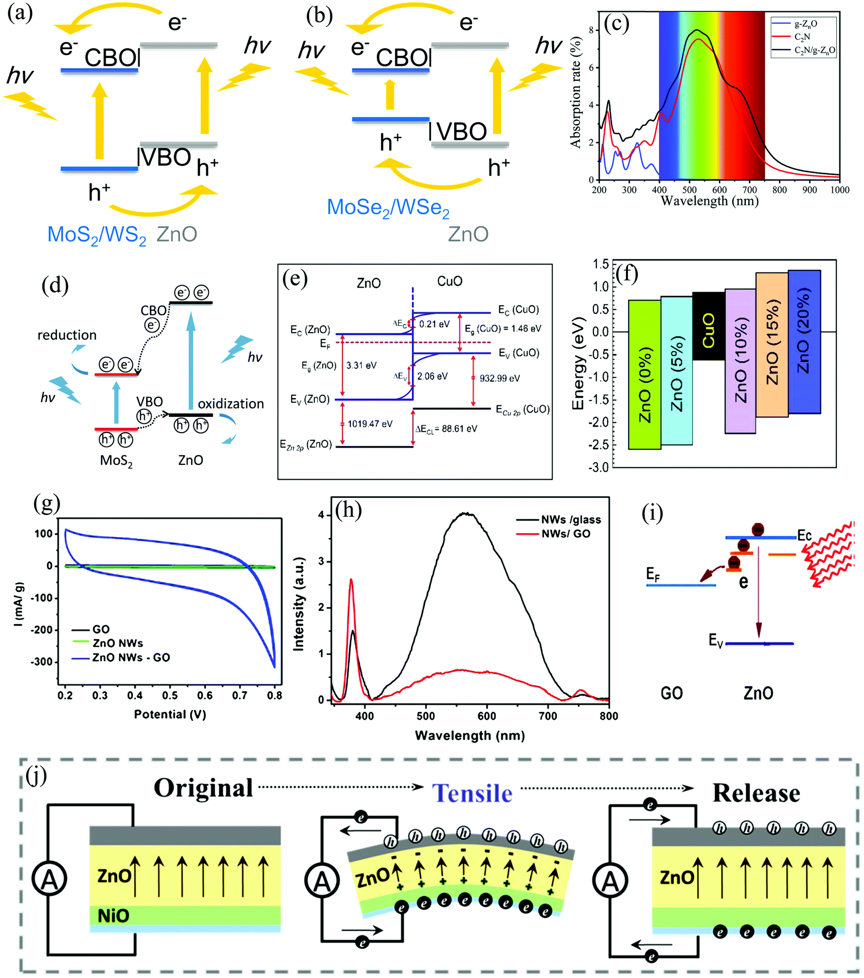 | ||
| Fig. 5 Schematic representation of photogenerated charge carrier motion in the HS of ZnO with (a) MoS2/WS2 and (b) MoSe2/WSe2.63 (c) Comparison of the absorption coefficient as a function of wavelength for a monolayer of C2N, ZnO, and their HS.65 (d) Schematic representation of photogenerated charge carrier motion in the HS of ZnO with MoS2 during photocatalysis.62 (e) Band diagram of the ZnO/CuO HS solar cell and the (f) schematic for the band offset for different levels of cobalt doping.59 (g) Comparison of the electrochemical behaviors (cyclic voltammetry, CV) of GO, ZnO NWs, and their HS.66 (h) Photoluminescence spectra of ZnO NWs grown on bare glass substrate and on GO film, and (i) and the associated e− transfer mechanism between excited ZnO and the GO sheets.66 (j) Piezo-polarized charge generation in ZnO for self-powering dynamic strain monitoring in an HS with NiO.64 [Reprinted by permissions from ref. 59, 62, 64, and 65 from The Royal Society of Chemistry, Reprinted by permission from Springer Nature: Sci. Rep., S. Wang et al., 8, 1–663 © 2018 and Springer Nature: Nanoscale Res. Lett., H. Zeng et al., 8, 133–13966 © 2013]. | ||
The range of advantages that ZnO HSs offer also extend to the field of electrochemical systems, such as that of supercapacitors (SC).61,66 Zeng et al., depicted the synergistic effect of ZnO HS on the electrochemical performance by growing ZnO NWs on thin graphene (Gr) oxide (GO) films.66 The increased specific capacitance in the ZnO/GO HS device (Fig. 5(g)) was a result of the three-dimensional structure, which resulted in rapid e− transfer between the active materials and the charge collector. The other synergistic effects were contributed by the one-dimensional architecture of the NWs. In addition, an increased UV emission and subdued visible emission (defect-related) was observed in the HS, as depicted in Fig. 5(h). Enhanced UV emission in the HS could arise from the high crystallinity of the NWs grown on GO, while the subdued visible emission could be from e− transfer between the two NSs (Fig. 5(i)). At the other end of the spectrum, an HS with a p–n junction has also proved to be an efficient self-powered vibrational sensor with application in the field of flexible electronics.64 Upon application of a horizontal tensile strain, the intrinsic piezoelectric property of ZnO leads to the generation of a piezopotential, and thus, a self-powering response (Fig. 5(j)). This intrinsic piezopotential, however, is revamped to reduce the interfacial leakage current by the p-NiO. The overall result is an enhanced piezopotential, and thus, increased self-powering response in the HS.64
The field of ZnO HSs has thus touched every aspect of science and technology, resulting in new discoveries and technological advancements. This review, however, focuses on the contribution of ZnO HSs toward next-generation devices that can operate independently and wirelessly, i.e., the so-called self-powered devices.71–73 In particular, the focus of this review article is to present the gradual progress in ZnO HSs from self-powering PDs to self-charging electrochemical capacitors. An emphasis is provided on analyzing the underlying mechanisms of the self-powering capability of ZnO along with its constituent interfaces in the PDs and electrochemical capacitors in the next two sections. Readers are also encouraged to read the very recent reviews covering the different aspects of self-powering technology.74–76
Self-powered zinc oxide heterostructure photodetector
 | ||
| Fig. 6 Schematic representation of the self-powering working mechanism of (a) Schottky type,77 (b) p–n junction type,82 and (c) PECC type85 PDs. [Reprinted by permissions from ref. 77 and 82 from The Royal Society of Chemistry and Reprinted from, J. Alloys Compd., Z. Bai and Y. Zhang, 675, 325–330,85 © 2016, with permission from Elsevier]. | ||
Fig. 6(c) schematically illustrates the working mechanism of a UV-Vis sensitive ZnO/Cu2O NW/electrolyte heterojunction-based self-powered PECC.85 In this work by Bai and Zhang, in addition to the self-powering response, an additional advantage was added to the cell by providing it a dual spectral sensitivity (UV + visible) with improved device performance achieved from the ZnO/Cu2O HS.85 Below, we discuss the utilization of these different mechanisms to achieve self-powering response in ZnO HS-based PDs.
Schottky junction-type self-powered zinc oxide heterostructure photodetector
Among several research groups, Prof. Abha Misra's group has a substantial contribution toward the progress in the research on ZnO-based self-powered PDs.87–90 Her group reported a Schottky junction-type self-powered UV PD with the HS of Gr and ZnO NWs.90 The self-powered assembly was fabricated by sandwiching the NWs in between two Gr layers (Fig. 7(a)); the HS optical image is depicted in Fig. 7(b). The role of ZnO is to act as the photosensitive layer, while the Gr layers act as the transparent electrode with the additional contribution of providing high mobility to the photogenerated charge carriers. A built-in electric field is generated at the interface of Gr and ZnO, which in turn provides the self-powering response. Gr was grown using atmospheric chemical vapor deposition (CVD @ 980 °C) in an inert atmosphere (Ar) with the decomposition of methane gas (20 standard cubic centimeter per minute (sccm) for 3 min) on copper (Cu) substrate. ZnO NWs were then grown directly on top of graphene (transferred on SiO2/(1 µm)/Si substrate) in a resistive thermal evaporator by evaporating Zn with the introduction of O2 gas under appropriate conditions.90Fig. 7(c) portrays an asymmetric current–voltage (I–V) characteristic of the device (Gr/ZnO/Gr) under both dark and UV conditions, with the inset depicting the same in the low bias region. Such a behavior is attributed to back-to-back Schottky barrier formation in the Gr/ZnO/Gr device configuration. The formed Schottky barrier owes its origin to the difference in the work function of graphene and the electron affinity of ZnO.90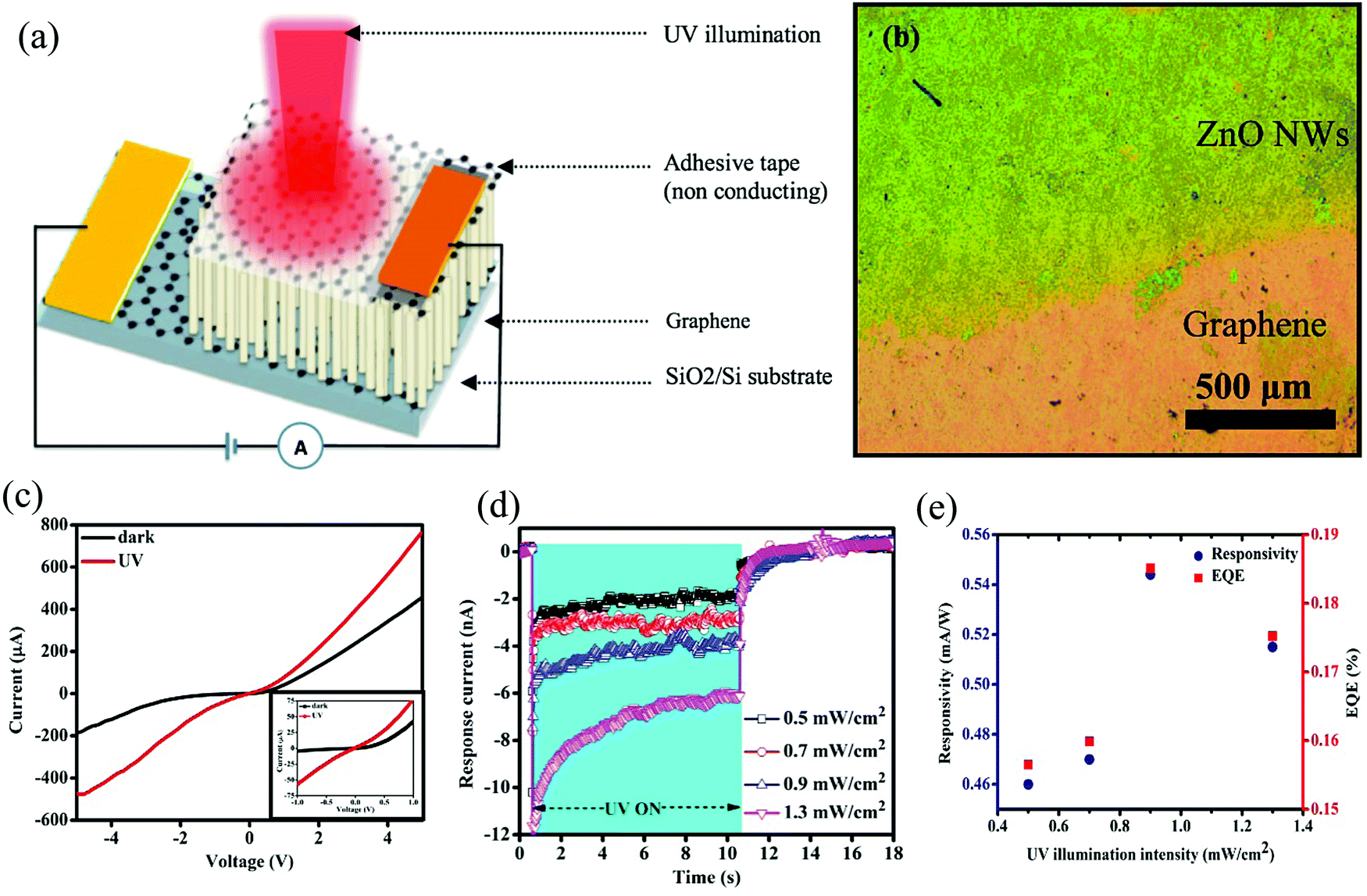 | ||
| Fig. 7 (a) Pictorial representation of the self-powered PD. (b) Optical image of the HS. (c) Device I–V characteristics both under dark (no illumination) and under UV (365 nm). (d) Self-powering temporal response (I–t) of the PD under varying illumination intensities. (e) External quantum efficiency and current responsivity (Ri) as a function of the illumination intensities.90 [Reproduced from ref. 90, Nanotechnology, B. D. Boruah et al., 27, 095205,90 https://doi.org/10.1088/0957-4484/27/9/095205, © 2016, with permission from IOP Publishing, Ltd]. | ||
The device self-powering response for different incident UV illumination intensities (0.5–1.3 mW cm−2) is depicted in Fig. 7(d). For the illumination intensity of 1.3 mW cm−2, the device exhibits a maximum self-powering photoresponse, with a response current of ∼6.7 nA. The increase in the response current with the incident intensity is a result of the proportionate relationship between the photogenerated carriers and the incident/absorbed photon flux.90 The other device parameters,such as the external quantum efficiency and Ri, as a function of the illumination intensities, are presented in Fig. 7(e). Under the self-powering response, a maximum Ri of ∼0.54 mA W−1 and an external quantum efficiency of ∼0.185% was achieved for the PD under 0.9 mW cm−2 of UV.
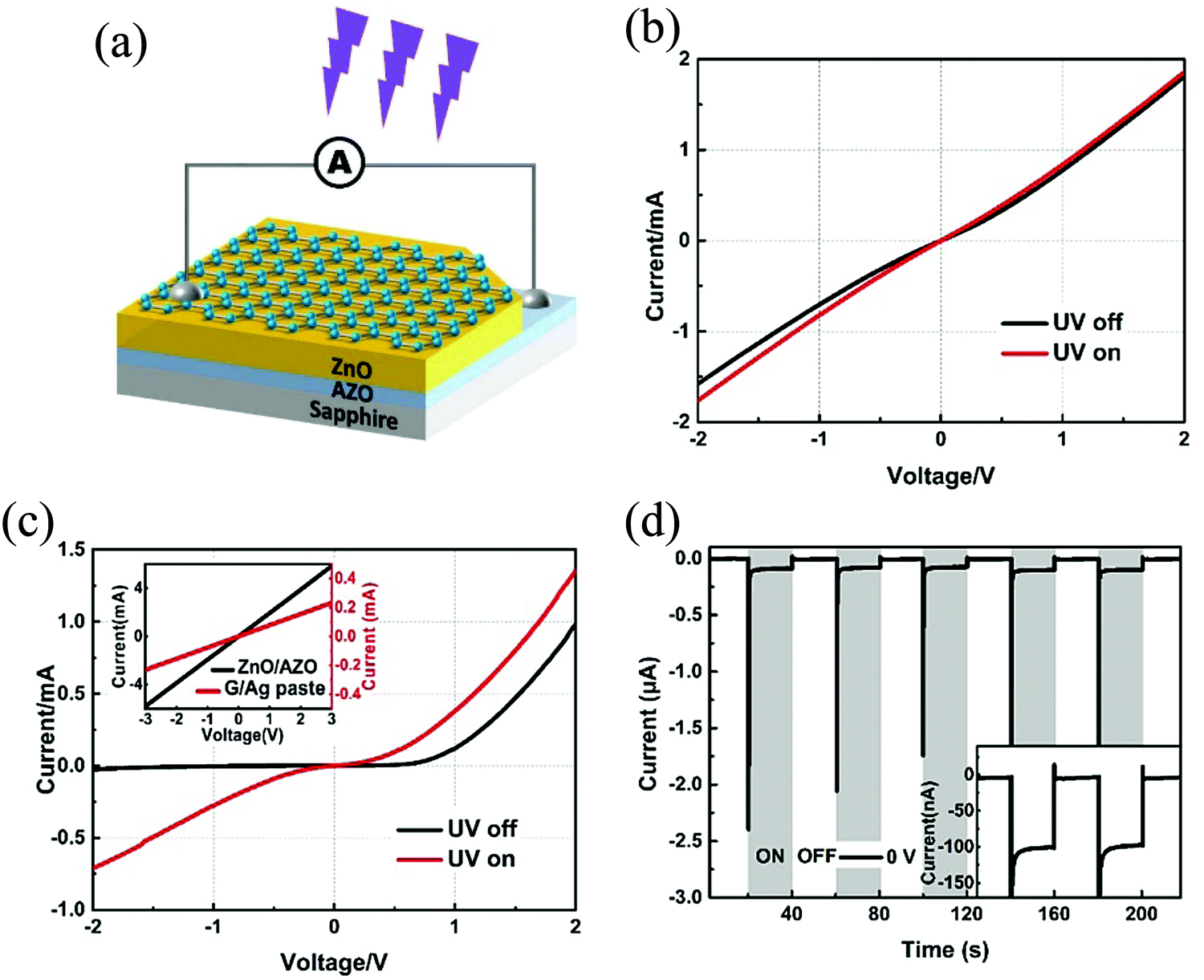
A Schottky junction-based self-powered UV PD was reported by Chen et al. with Gr and modified ZnO.91 Ideally, in accordance with the Mott–Schottky theory, undoped Gr (work function of 4.6 eV) and undoped ZnO (work function of 4.4 eV) form a Schottky barrier upon contact.92 However, many existing reports show that in a practical scenario, the contact is rather ohmic or quasi-ohmic.91,93,94 The occurrence of this non-ideal behavior arises from the surface defect states in the ZnO Eg, thereby resulting in the pinning of the Ef.91 To overcome this problem, the surface modification of ZnO is suggested, which in the work of Chen et al., was achieved via RT surface treatment of the ZnO film using H2O2. A similar idea for stabilizing the Schottky barrier was also proposed and depicted by Duan et al., in a surface-treated Gr/ZnO:Al NR-array-film structure.95 The self-powered PD architecture of Chen et al., with the configuration as Gr/ZnO/AZO (Al doped ZnO) is presented in Fig. 8(a). Both ZnO as well as the AZO films were grown on sapphire substrates via pulsed laser deposition. The deposition was carried out using a 248 nm krypton fluoride excimer laser with a pulse power of 300 mJ and a repetition rate of 4 Hz. The surface modification of the as-grown ZnO/AZO film was then carried out by immersing in 30% H2O2 at RT (H-ZnO/AZO) for 15 min. The overall thickness of the film was ∼300 nm, with ∼200 nm of ZnO and ∼100 nm of AZO with the H-ZnO/AZO film, on the other hand, depicting a rugged surface. Gr, grown on Cu foil by CVD, was then transferred on top of this surface-modified ZnO film via the wet-transfer route. The device was then finally completed with Ag as one of the metal contacts in Gr and indium as the other one on AZO.
 | ||
| Fig. 8 (a) PD device configuration. I–V characteristics of (b) Gr/ZnO/AZO and (c) Gr/H-ZnO/AZO device (inset is for ZnO/AZO and Gr/Ag contact devices) under dark and UV. (d) Self-powering response of the Gr/H-ZnO/AZO device.91 [Reprinted by permission from Elsevier: Appl. Surf. Sci., D. Chen et al., 529, 14708791 © 2020]. | ||
The I–V characteristics (both under dark and UV) depicted a quasi-ohmic/ohmic behavior for Gr/ZnO (Fig. 8(b)), ZnO/AZO, and Gr/Ag contact devices (inset of (Fig. 8(c))). On the other hand, the Gr/H-ZnO/AZO device showed a rectifying behavior (Fig. 8(c)), and thus, a self-powering response (Fig. 8(d)). The I–t graph in Fig. 8(d) presents a cyclic response with contributions from both the built-in electric field as well the pyroelectric potential (the sharp peaks), the so-called pyro-phototronic effect, an effect arising from light-induced rapid temperature increase of ZnO.91,96 An Ri of 50 µA W−1 with a response (tr) of recovery times (tf) each of 32 ms was obtained for the self-powered PD.91
Another promising material for forming an HS with ZnO for self-powering response is GaN, which has properties closer to ZnO. Both ZnO and GaN have a lot in common as both are wurtzite semiconductors with nearly the same direct Eg (∼3.37 eV and 3.41 eV), high cohesive energy (1.89 eV2 and 9.16 eV2), lower lattice mismatch (1.9%), large exciton binding energy (60 meV and 24 meV), and spontaneous polarization (0.047 cm−2 and 0.029 cm−2), respectively, as provided by Mishra et al.97 A ZnO/GaN HS UV detector was reported by Mishra et al., as shown in the schematic of Fig. 9(a).
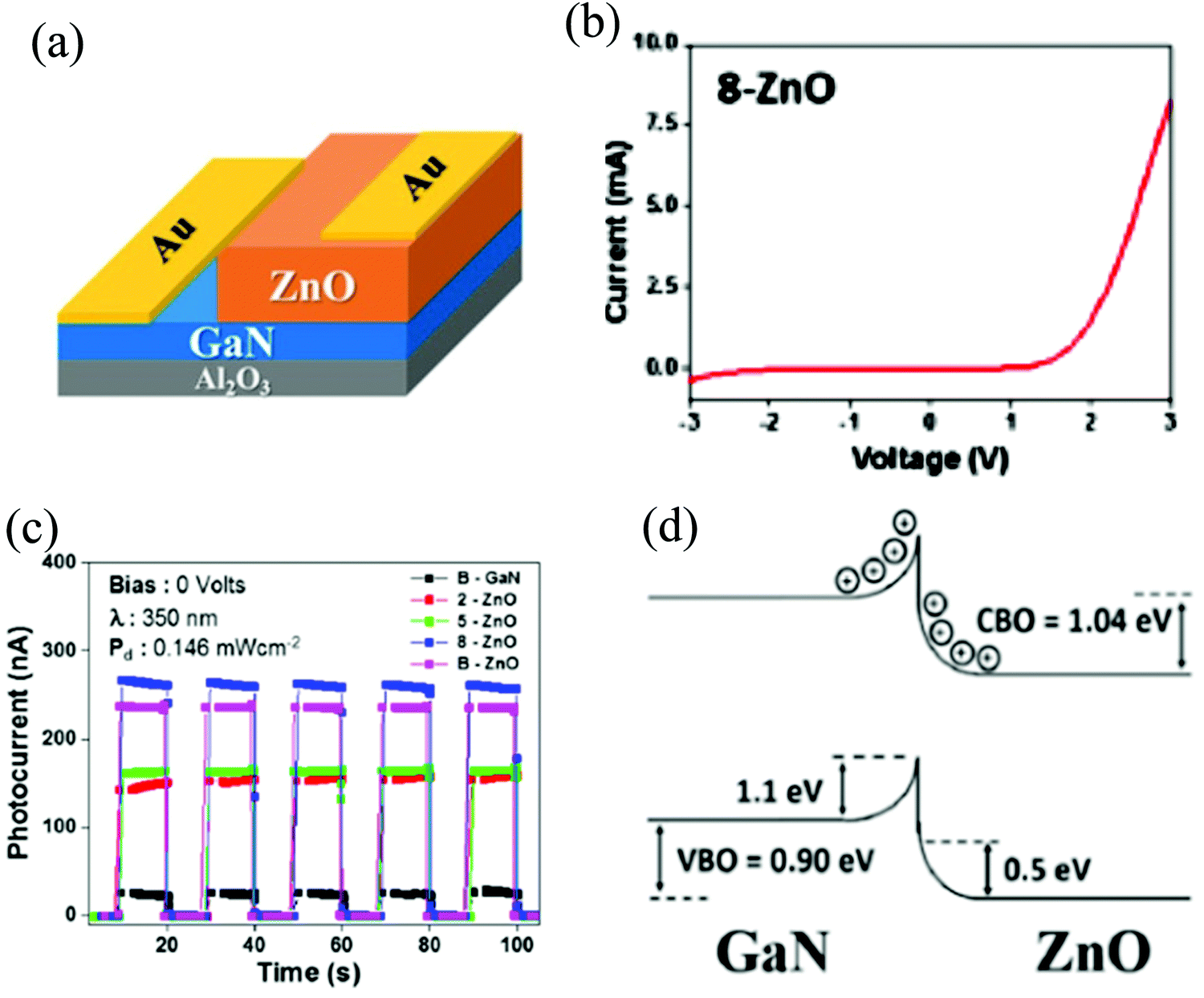 | ||
| Fig. 9 (a) ZnO/GaN self-powered PD schematic. (b) The I–V curve of the HS device for an optimized ZnO thickness. (c) Photoresponse at zero-bias for different devices at 350 nm illumination. (d) Schematic representation of ZnO/GaN interfacial band bending.97 [Reprinted from ref. 97, Appl. Surf. Sci., M. Mishra et al., 478, 1081–1089,97 © 2019, with permission from Elsevier]. | ||
The HS forms a Schottky junction with the interfacial properties and thus the photosensitivity is dependent on the thickness of the deposited ZnO film. The interfaces were fabricated by growing varied thicknesses of ZnO films on a highly crystalline 3.5 µm-thick GaN layer (as substrate) at 300 °C. The device schematic and the corresponding I–V characteristics are depicted respectively in Fig. 9(a) and (b), portraying the Schottky behavior for an optimum ZnO film thickness (named as 8-ZnO).97 Upon UV illumination, the measured self-powered Ri of the device was 95.8 mA W−1 with a visible-blind photosensitivity. The dynamic photoresponse of the self-powered PD is depicted for various thicknesses of the ZnO film (Fig. 9(c)) at a wavelength of 350 nm with the 8-ZnO device depicting the highest response. Moreover, due to nearly the same Eg of GaN and ZnO (as mentioned earlier), the highest device self-powering Ri was obtained in the range of 360–380 nm.97Fig. 9(d) schematically shows the interfacial band bending/offset in the HS.97
In addition to self-powering, a report by Benyahia et al. also presented a multispectral broadband self-powering response based on a ZnO/ZnS microstructure composite (MC), as depicted in Fig. 10(a).98
 | ||
| Fig. 10 (a) Device schematic and (b) I–V characteristics of the device under dark and various light illumination. (c) Zero-bias light switching behavior of the device. (d) Figure of merit (FoM) comparison of the device for all the incident wavelengths.98 [Reprinted from ref. 98, J. Alloys Compd., K. Benyahia et al., 859, 158242,98 © 2020 with permission from Elsevier]. | ||
The composite was first grown by the thermal evaporation of ZnS on a glass substrate and then subsequently annealing the film in air at 500 °C for 1 h to form the top layer ZnO. The final device in a metal-semiconductor–metal configuration (Schottky type) was then fabricated with gold (Au) contact deposition via e-beam evaporation (Fig. 10(a)).98 Upon optical characterization of the MC film, it was observed that the film depicted an enhanced optical absorption. Such enhanced absorption was due to light trapping and thereby optical confinement effects arising from the surface granulation, together with the presence of void spaces. The electrical characteristics, on the other hand, displayed a different picture with a voltage offset of 0.15 V under the illumination condition (Fig. 10(b)), thereby prompting the self-powering operation. Such an offset was a result of the built-in electric field in the ZnO/ZnS HS. The opto-electrical behavior upon light switching is depicted in Fig. 10(c), where under zero-bias, the tr/tf were 22.5/45.2 s, 22.3/40.1 s, and 25.2/15.6 s, respectively, for the detection of UV, visible, and near IR, respectively. Fig. 10(d) compares the device parameters for all the illumination wavelengths, and it is observed that the FoM is the highest for UV illumination as it corresponds to the Eg of ZnO.
In another study, ZnO/Au/Al2O3 PDs with increased UV detection for self-powering response was reported. The surface of Au nanoparticle (NP)-decorated ZnO NRs was covered with a thin layer of Al2O3, utilizing atomic layer deposition to form the ZnO/Au/Al2O3 core–shell NRs. The schematic of the as-fabricated PD is presented in Fig. 11(a). From the high-resolution transmission electron microscopy (HRTEM) images, adjacent lattice fringes of 0.28 and 0.235 nm were observed, which corresponded respectively to the (110) and (111) plane of ZnO and Au.99,100Fig. 11(b) depicts the I–V of both ZnO/Al2O3 and ZnO/Au/Al2O3 devices measured both under dark and 365 nm illumination. A rectifying behavior is depicted by the ZnO/Au/Al2O3 PD (under both dark and UV conditions) with enhanced current in the illumination (365 nm) state. The I–t curve at different incident power intensities is depicted in Fig. 11(c), where the response of the ZnO/Au/Al2O3 device is higher compared to that of only the ZnO/Al2O3 device. The ZnO/Au/Al2O3-based self-powered PD showed a Ri of 6.8 mA W−1 and a detectivity of 1.7 × 10⁹ Jones, which were respectively 8.6 and 8.5 times that of the ZnO/Al2O3-based PD (Fig. 11(d)) at a light intensity of 0.6 mW cm−2.
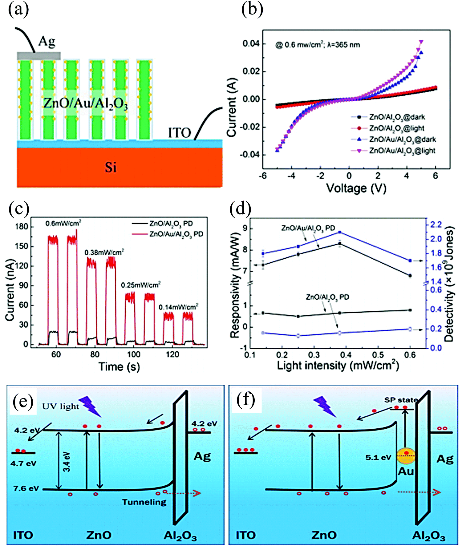 | ||
| Fig. 11 (a) Device schematic and (b) I–V characteristics at a fixed intensity and (c) I–t curves of the self-powered ZnO/Al2O3 and ZnO/Au/Al2O3 PDs under 365 nm light illumination with different light intensities. (d) Ri and detectivity of the self-powered ZnO/Al2O3 and ZnO/Au/Al2O3 PDs. Self-powering working mechanism of (e) ZnO/Al2O3 and (f) ZnO/Au/Al2O3 devices under the illumination condition.100 [Reprinted by permission from Springer Nature: J. Mater. Sci. Mater. Electron., F. Cao and X. Ji, 31, 2657–2665100 © 2020]. | ||
In the report, it was suggested that after the excitation of the e−s from the VB to the CB (due to UV), few energetic e−s have a large probability to transfer to the ITO Ef, while others may recombine with the h+s in the ZnO VB without actually passing through the Al2O3 layer. The photocurrent was obtained from the h+s tunnelling through the Al2O3 layer and finally reach Ag electrode without combination.101 However, with the Au NP-decorated PD, an enhanced light absorption was obtained, arising from the surface plasmon resonance along with hot e−s.102 Hence, more e−s are transferred to the ITO electrode via the ZnO CB. The Au NP decoration resulted in a charge transport to enhance the photodetection performance of the device.100Fig. 11(e) and (f) schematically depicts the energy band diagram and the proposed operating mechanism of the self-powered PDs discussed in this work.
Technological advances have also been proposed in this direction, with the introduction of flexible self-powered PD.103 In a work by Sinha et al., they fabricated a self-powered UV PD with carbon dot (CD)-enhanced ZnO/graphite HS on a flexible cellulose paper (Fig. 12(a)).103 The ZnO NRs were directly grown on graphite-coated cellulose paper via a hydrothermal technique. They first started with pencil sketching a cellulose paper for forming a layer of graphite, which was then sequentially dipped (in a ZnO precursor solution) and dried (100 °C for 15 min). The precursor solution was prepared by dissolving (along with stirring) 0.01 M of zinc acetate dihydrate in 50 mL isopropyl alcohol (65 °C for 1 h) along with 0.02 M diethanolamine. The dried cellulose paper was then subjected to hydrothermal treatment (90 °C for 6 h) in a solution made by mixing hexamethylenetetramine (0.05 M) and zinc nitrate hexahydrate (0.05 M). Finally, the NRs grown on cellulose paper were heated overnight at 50 °C for getting better crystalline rods. For the final device, the CDs, synthesized via the microwave-assisted hydrothermal method of tobacco, were anchored to the NRs by dipping the NRs for 2 h in the CD solution.103 The electrical behavior (I–V) of the device portrays diode-like characteristics (both under dark and light) along with the photovoltaic effect (Fig. 12(b)). A current offset of 19 nA under dark (which increased under UV) was observed, thus prompting the self-powering response (Fig. 12(c)).
 | ||
| Fig. 12 (a) Pictorial representation of the PD with the inset photograph depicting the flexible nature of the device. I–V characteristics of the device (both dark and under UV) in (b) linear and semilogarithmic scale (inset) along with (c) enlarged depiction near the 0 V regime. (d) Schematic representation of ZnO/graphite interfacial band bending and formation of Dr at zero-bias. (e) Mechanism of self-powered photocurrent generation in the Schottky diode PD.103 [Reprinted with permission from R. Sinha et al., ACS Appl. Mater. Interfaces, 12, 33428–33438103 © 2020 American Chemical Society]. | ||
Temporal characteristics (I–t) of the device under zero-bias condition depicted tr and tf of ∼2 and ∼3.2 s, respectively. The self-powering mechanism of the PDs is attributed to the Schottky junction formation between ZnO and graphite, with each having respective work functions of 4.4 and 5 eV.103 The band diagram of the HS under zero-bias condition is depicted in Fig. 12(d). This work, in addition to exploring the self-powering response of the HS (ZnO and graphite), also introduces the effect of an additional HS, i.e., CD with ZnO, to achieve enhanced photoresponse.103 According to the authors, the anchored CDs are also UV responsive, and thus upon UV incidence, generate additional e−–h+ pairs that further contribute to the total photocurrent. The proposed mechanism of photocurrent generation in the final device with CDs under zero-bias condition is depicted in Fig. 12(e). The photogenerated e−s in the CD jump to the CB of ZnO while the remaining h+s get trapped in the trapping sites of ZnO, thus resulting in an overall reduction of e−–h+ recombination. The overall result was an increased photocurrent. The other possibility of the CD h+ dynamics that the authors point to is the increase in O2 desorption (in ZnO) by the photogenerated h+ in the CD. In addition, the authors also attribute the self-powering response of the PD to the associated pyro-phototronic effect in the NRs.103 The claim on the device flexibility, and thus its robustness toward mechanical deformation, was supported by presenting the variation of the ON/OFF current ratio (ION/IOFF) under different bending cycles. It was observed that even after 50 cycles of bending, the photodiode preserved more than 90% of ION/IOFF as compared to the first cycle. This observation thus supported the claim of the authors on the design and demonstration of a ZnO HS-based self-powered flexible UV PD.103
p–n junction-type self-powered zinc oxide heterostructure photodetector
The second type of HS architecture that has the ability to exhibit self-powering response is the p–n junction type with ZnO acting as the n counterpart of the junction.88 Recently, Lin et al. demonstrated p-type Cu2O/ZnO NRs in a stack for self-powered photoresponse in the range of UV to visible (570 nm).104 Both the semiconducting materials provide a good energy level alignment necessary to generate the built-in electric field (the Eg of Cu2O is 1.9–2.2 eV). The stack consists of a Cu2O film of ∼430 nm thickness, a ZnO seed layer of 20 nm thickness, and vertically aligned ZnO NRs of ∼2.5 µm length. The I–V plots of the p-Cu2O/n-ZnO PD within a bias sweep of −1 to +1 V under dark and illumination (UV and visible) conditions depict a rectifying behavior. The self-powered Ri of the PD was 0.24 A W−1 and 0.06 A W−1 at 380 and 450 nm, respectively. Furthermore, at zero bias, the tr and tf under 370 nm illumination were reported to be 0.02 s and 0.03 s, respectively. From the energy band diagram at no bias voltage, it was observed that under UV illumination, e−–h+ pairs are generated in the depletion layer, which then quickly get separated by the built-in electric field. Due to the built-in electric field, the e−s and h+s are respectively transported toward n-ZnO and p-type Cu2O, thereby leading to photocurrent generation.104 Further, a nanoscale interface fabricated with n-type ZnO NW on p-type GaN film was studied for a self-powered UV detector.81 The nanoscale heterojunction is shown in Fig. 13(a).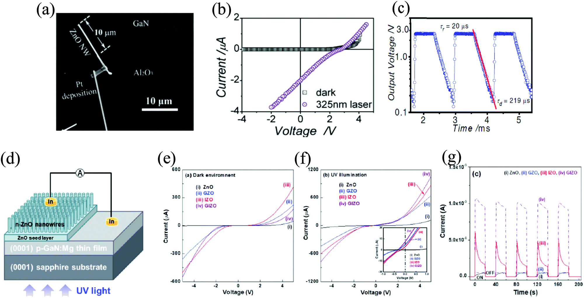 | ||
| Fig. 13 (a) Scanning electron microscope (SEM) image of n-type ZnO NW/p-type GaN film heterojunction. (b) I–V curves of the NW/film heterojunction under dark and UV illumination. (c) Photo voltage of the heterojunction plotted with time. (d) Device schematic and I–V characteristics (e) under dark and (f) with UV illumination (inset depicting open-circuit voltage and short-circuit current during the illumination). (g) Self-powering response of all the devices.81,108 [Reprinted by permission from John Wiley and Sons: Adv. Mater., Y. Q. Bie et al., 23, 649–65381 © 2011 and Reprinted from ref. 108, C.-Y. Tsay et al., Mater. Sci. Semicond. Process., 121, 105295,108 © 2020, with permission from Elsevier]. | ||
The self-powered, visible-blind UV PD exhibited a tr and tf of ∼20 and ∼219 µs, respectively, with faster response than ZnO alone by two orders of magnitude. Under dark, a rectification characteristic was observed with a threshold voltage of ∼3 V (Fig. 13(b)) and a current of <1 pA, whereas in the presence of light, the photocurrent was ∼2 µA. The temporal response of the output voltage on a logarithmical scale is presented in Fig. 13(c). From the response, a decay time (τd) of 219 µs was obtained. The obtained time was smaller than that already reported for photoconductive105 and Schottky junction UV detectors.106,107 In a NW PD, the surface modification strongly enabled prolonged photoresponse, and thus, improved the PD performance, while surface passivation is desirable.81
Further development on ZnO/GaN-based self-powered PDs was reported by Tsay et al. by co-doping ZnO with gallium (Ga) and indium (I). The hydrothermal method was used to fabricate Ga-In co-doped ZnO (GIZO)-based self-powered PD on sapphire/p-GaN at low temperature, as presented in the schematic of Fig. 13(d). All the devices (undoped, single doped, as well co-doped) showed rectifying I–V characteristics under both dark and light (Fig. 13(e) and (f)). However, under light (UV), a degradation in the rectifying nature was observed with an offset at 0 V (Fig. 13(f)). Thus, it was observed that the self-powered response of the p-GaN/n-GIZO heterojunction exhibited superior performance compared to other devices with an Ri of 5.29 mA W−1. The self-powering response is due to the induced built-in electric field by the p–n junction (Fig. 13(g)).108 Apart from exploring this HS (ZnO/GaN) for self-powering UV PD, researchers have also demonstrated techniques to further improve its self-powering response via the insertion of the CdS layer.109 The idea here is to introduce a p–i–n type heterojunction, where the role of CdS is to act as an “i-type” layer, and thus further reduce the interfacial charge recombination along with assistance in charge transport.109
Another self-powered PD based on the HS array of metal oxide, NiO/ZnO-NR, is studied for the UV detection performance under zero bias condition. Both n-type ZnO NR array and p-type NiO film were synthesized via chemical method. The device schematic is presented in Fig. 14(a), where the ZnO NR arrays were grown hydrothermally on NiO thin films via the nucleation sites from the ZnO seed coated on top of the NiO film. The metal contacts were made from Au and silver (Ag), with Au being deposited onto the NiO film and Ag paste on the ZnO NRs array side.
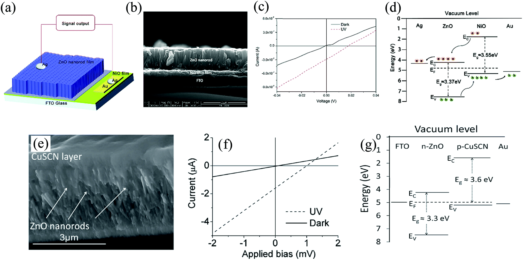 | ||
| Fig. 14 (a) Depiction of the p-NiO/n-ZnO NRs array PD device configuration along with its (b) cross-sectional morphology using SEM. (c) The I–V curve both under dark and UV. (d) Heterojunction band-diagram depicting the detection mechanism. (e) Microstructure of ZnO NRs with the CuSCN layer on the top. (f) I–V curve for both dark and UV illumination conditions. (g) Energy-band diagram of the ZnO/CuSCN HS device.110,111 [Reproduced with permission from ref. 110 from The Royal Society of Chemistry and Reprinted by permission from John Wiley and Sons: Adv. Mater., S. M. Hatch et al., 25, 867–871111 © 2013]. | ||
The cross-sectional morphology of the p-NiO/n-ZnO NR array is depicted by the SEM image in Fig. 14(b). The I–V characteristics of the device both under dark and illumination (355 nm UV, intensity ∼3.2 mW cm−2) is shown in Fig. 14(c). Under UV, an offset in the current is observed due to the photovoltaic effect; this thus contributes to the self-powering performance of the detector. The origin of such zero bias response is attributed to the generated built-in electric field from the interfacial interaction of ZnO and NiO arising from the energy band alignment (Fig. 14(d)). This band alignment helps in the separation of the e−–h+ pairs photogenerated in ZnO to the respective electrodes for photocurrent generation.110 The same HS was also further explored by Bhatnagar et al., for photovoltaic memory with application in a transparent neuromorphic device.58 Along with transparency, the device exhibited additional features of self-powering toward light detection and memristive operation as well.58
The n-type ZnO NRs array was further utilized for self-powered PD in conjunction with p-type copper thiocyanate (CuSCN) to form a p–n heterojunction. Under an UV irradiance of 6.0 mW cm−2, the self-powering photocurrent was 4.5 µA. The observed photoresponse was much higher than that of most reported ZnO HSs. ZnO NRs with a diameter in the range of ∼70–100 nm and height ∼2–3 µm was coated with a thin film of CuSCN, as can be seen from the device's cross-sectional microstructure in Fig. 14(e). The I–V plot in Fig. 14(f) shows a rectification behavior, with a ∼0 V turn-on voltage under UV, arising from the photovoltaic effect. The well-aligned band structure from fluorine-doped tin oxide (FTO) to Au (Fig. 14(g)) results in the observed self-powering response. This intrinsic alignment prevents the photoexcited e−s in ZnO from recombining with h+s at the junction, thereby allowing efficient interfacial charge-carrier separation.111
Cao et al., in their previous work demonstrated a Schottky type self-powered UV PD based on ZnO/Au/Al2O3, which was further extended to a p-n type one based on an HS of n-ZnO/p-CuI/Au (Fig. 15(a)).112 The rationale behind using this particular device architecture is to explore the HS property for the self-powering response along with the synergy of Au plasmonic response to enhance the overall obtained photoresponse. Fig. 15(b) shows the cross-sectional view of the HS, with the grain dimensions and thickness of respectively 50–60 nm (ZnO)/400–500 nm (CuI) and ∼150 nm (ZnO)/∼350 nm (CuI), respectively. The presence of Au was confirmed using different characterization techniques such as X-ray diffraction and energy-dispersive X-ray spectroscopy.112
 | ||
| Fig. 15 (a) Device schematic and (b) the HS cross-sectional view. (c) I–V characteristics of the devices both in dark and UV. (d) Self-powering I–t of the ZnO/CuI and ZnO/CuI/Au PDs. (e) HS (ZnO/CuI) energy band diagram and the principle of operation in the (f) ZnO/CuI/Au HS under UV.112 [Reprinted from ref. 112, F. Cao et al., J. Alloys Compd., 859, 158383,112 © 2020, with permission from Elsevier]. | ||
The I–V characteristics of the devices (ZnO/CuI and ZnO/CuI/Au, Fig. 15(c)) depict the rectifying behavior under both dark and UV (365 nm). The self-powering I–t shows a good stability and periodicity for both the HS devices with the HS, with Au depicting ∼3.44 times higher response compared to that without Au (Fig. 15(d)).112 The tr and tf are respectively 0.41 s (ZnO/CuI)/0.41 s (ZnO/CuI/Au) and 0.24 s (ZnO/CuI)/0.08 s (ZnO/CuI/Au). The energy band alignment in ZnO/CuI and the consecutive enhancement in the photoresponse after the incorporation of Au are respectively depicted in Fig. 15(e) and (f). A built-in electric field was generated when ZnO is brought in contact with CuI, thus helping in the self-powering response upon UV illumination. On the other hand, when Au is incorporated in the HS, the plasmonic effect comes into the picture with the excitation of hot e−s to the CuI CB. The excited hot e−s transport toward the ZnO CB and in turn leads to an increase in the photocurrent. The adopted technique in this work thus provides additional insights into the field of ZnO HS-based self-powered PDs by coupling with plasmonics.112
A further extension in the direction of these p–n junction type ZnO HS-based self-powered UV detectors was to realize a broadband self-powering capability, and was demonstrated in a core–shell NW system of ZnO–Co3O4 by Ghamgosar et al.113
Co3O4 was chosen because of its two direct bandgaps (1.5 and 2.2 eV) for light absorption in a single p–n junction photovoltaic device.114,115 In addition, the electronic band structure of Co3O4 matched well with the position of ZnO CB at the heterojunction interface.116–118 The ZnO NWs (Fig. 16(a)) were prepared by the hydrothermal technique and a reactive dc magnetron sputtering (applied constant power of 70 W) was used for depositing the Co3O4 layer on the NWs (Fig. 16(b)). The deposition gas was made from a mixture of highly pure argon (95%) and oxygen (5%) at a flow rate of 25 sccm. The I–V curve in Fig. 16(c) portrays a rectifying behavior (asymmetrical I–V shape) under dark due to the p–n junction formation at the interface of ZnO and Co3O4. Fig. 16(d) shows the self-powering photoresponse of the core–shell for varying the Co3O4 thickness (1, 8, 10, and 15 nm). Among all the devices, the device with 1 nm coating (the thinnest one) showed the highest response to light. On the other hand, increasing the thickness of the Co3O4 layer led to a decrease in the photoresponse. Photocurrent increase was due to the increased temperature and decrease in the surface depletion depth arising from light illumination. Moreover, in this work, in addition, a system of ZnO–Al2O3–Co3O4 was also studied where Al2O3 acted as the passivation layer. Under zero bias, the ZnO–Al2O3–Co3O4 system depicted a photoresponse that was six times higher compared to the pristine core–shell (ZnO–Co3O4).113
 | ||
| Fig. 16 SEM image of (a) bare ZnO NWs and (b) ZnO NWs-Co3O4 core–shell. (c) I–V characteristics of the core–shell under dark (dashed lines) and illumination (solid lines) with varying Co3O4 thickness (inset depicts zoomed-in curves). (d) Zero bias temporal response (I–t) response of the structure for varying Co3O4 thicknesses (inset shows the zoomed-in image within the current interval of 0 to −1.5 nA).113 [Reprinted with permission from P. Ghamgosar et al., ACS Appl. Mater. Interfaces, 11, 23454–23462113 © 2019 American Chemical Society]. | ||
A facile, low-cost, and greener fabrication technique was recently demonstrated by Zhang et al. for paper-based self-powered UV detector.119 The HS explored in this study was that of p-tellurium (Te) and n-ZnO, which formed a type-II heterojunction, and the device was fabricated by brushing the nanomaterials onto a paper. Te NWs (Fig. 17(a)) were synthesized via a hydrothermal technique using TeO2, KOH, glycol, PVP, and ascorbic acid while the ZnO nanoparticles (NPs) were commercially purchased (Fig. 17(b)). The microstructure of the wires, with a mean diameter of 30–60 nm and a length >10 µm, is depicted in Fig. 17(a), while cuboid ZnO NPs with sizes in the range of 200–300 nm are presented in Fig. 17(b). For Te NWs synthesis, TeO2 (0.165 g), KOH (0.167 g), and glycol (30 mL) were added and heated under stirring at 85 °C. PVP (0.1 g) was then added to the transparent solution under constant stirring with the further addition of ascorbic acid (1.5 mL) till the whole solution turned yellow. The final yellow solution was then subjected to hydrothermal process by transferring it into an autoclave at 150 °C for 6 h. After the process completion, the autoclave could cool down to the RT by itself, and the NWs were then obtained using centrifugation and cleaning. The as-obtained NWs were then dispersed in alcohol along with the ZnO NPs to form the HS.119
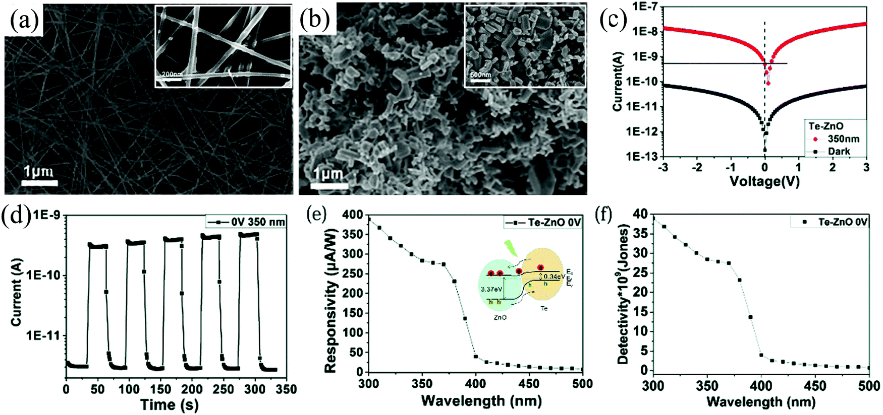 | ||
| Fig. 17 SEM images of (a) Te NWs and (b) ZnO NPs (both insets in (a) and (b) depict their respective high magnification images). (c) I–V characteristics of the Te–ZnO p–n junction both under dark and UV (350 nm). (d) Temporal (I–t) self-powering response of the HS. (e) Spectral Ri and (f) detectivity variation as a function of the wavelength at zero-bias. Inset of (e) depicts the energy band diagram of Te–ZnO HS under the illumination condition.119 [Reproduced with permission from ref. 119 from The Royal Society of Chemistry]. | ||
The I–V characteristics of the HS are presented in Fig. 17(c), which depicts a self-powering response, as portrayed by the current offset at zero voltage under UV. On exploring this property, the device I–t curve presents stable cyclic response, with an ON/OFF ratio of ∼100 (Fig. 17(d)) and tr/tf of 2.46/1.75 s. The self-powering spectral response shows that the PD exhibits a maximum Ri of 387 mA W−1 (Fig. 17(e)) and detectivity of 4 × 10¹⁰ Jones (Fig. 17(f)) at a wavelength of 300 nm. The self-powering mechanism of the device is depicted in the inset of Fig. 17(e), where a type-II heterojunction was formed between Te and ZnO, thus leading to the generation of a built-in electric field that assists the transport of the photogenerated charge carriers in the absence of any external bias.119
Till now, we discussed the heterojunctions between inorganic semiconductors; nevertheless, similar ideas can be extended for HSs formed by inorganic and organic semiconductors, as demonstrated by Misra's group.87–89 One such example is the junction formed between n-type ZnO and p-type poly(3,4-ethylenedioxythiophene)-poly(styrene sulfonate) (PEDOT:PSS) semiconductors.
In one of their works,88 they doped ZnO NRs with chlorine (Cl:ZnO) to enhance the free charge carrier density and thus effectively improved the self-powering response (∼333% improvement). The doping of Cl atoms via the hydrothermal route (Fig. 18(a)) results in increased charge carrier density and thus improved pyro-phototronic effect for self-powering response.88 Cl:ZnO was synthesized hydrothermally on ITO-coated glass, thereafter spin-coating 10 µL of PEDOT:PSS on top of that with the final metal contact of Ag on PEDOT:PSS (Fig. 18(b)). Thereafter, illuminating the device with 365 nm UV radiation resulted in a pyro-phototronic assisted self-powering response (Fig. 18(c)) with an Ri of 2.33 mA W−1 at zero bias. Furthermore, the response current increased with the increase in the UV illumination intensity (Fig. 18(d)) with a major contribution from pyrocurrent (∼1.6 times higher than photocurrent at 3 mW cm−2). The PD also displayed an outstanding fast self-powering with tr and tf of 28 and 23 ms, respectively (Fig. 18(e)). Finally, from the spectral response, it was observed that the device was visible-blind and was responsive only to UV, as shown in Fig. 18(f).88
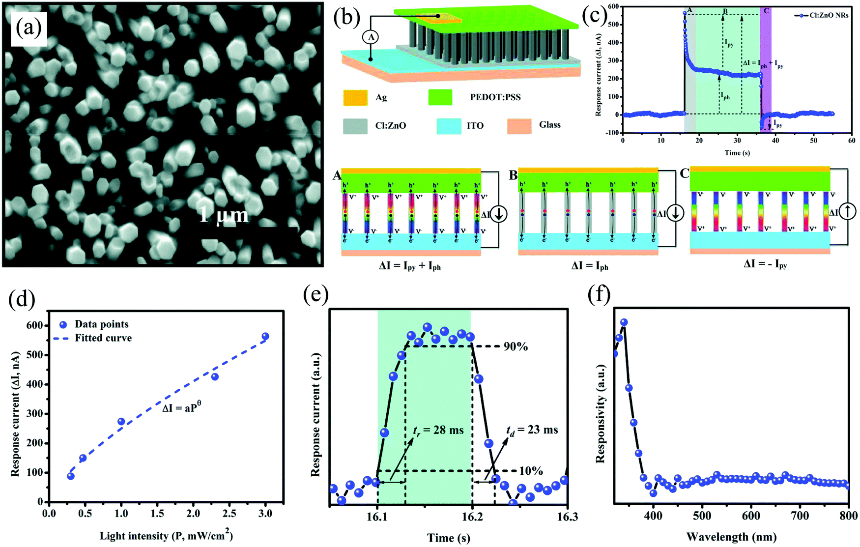 | ||
| Fig. 18 (a) SEM of Cl:ZnO NRs. Self-powered (b) device schematic along with (c) self-powered I–t response of the PD after UV illumination (365 nm, 3 mW cm−2). Stage-wise (A, B, and C) photoresponse mechanism as observed in the temporal response (c). (d) Response current variation with varying illumination intensities. (e) The tabulation of tr and tf under self-powering condition. (f) Spectral response characteristics of the device.88 [Reproduced with permission from ref. 88 from The Royal Society of Chemistry]. | ||
 | ||
| Fig. 19 (a) The I–V characteristics of the nanocomposite device under dark and UV (left inset represents the contrast ratio and the right represents the rectification ratio). (b) Self-powering response of the device under varying light intensities. (c) Energy band diagram under (i) dark and (ii) under illumination.120 [Reprinted from ref. 120, L. Ghorbani and S. Nasirian, Appl. Surf. Sci., 527, 146786,120 © 2020, with permission from Elsevier]. | ||
Moreover, a flexible self-powered UV PD was reported by Ghorbani et al., with n-ZnO and p-type polyaniline (PANI) nanocomposite.120 The hydrothermal technique was utilized to grow ZnO NRs in the composite. In their technique, initially, sodium hydroxide (3.84 g) and cetyltrimethylammonium bromide (0.146 g) were dissolved in 50 mL distilled (DI) water and mixed for 3 h at RT. To the resultant mixture, zinc nitrate hexahydrate (4.64 g) and stirred similarly at RT to obtain a colloidal solution. The hydrothermal process was then carried out by transferring the colloid into an autoclave (Teflon lined) and subjected to 110 °C for 12 h.120 The sample obtained at the end of the process was then cleaned, dried (120 °C), and calcinated (600 °C) to finally obtain the ZnO NRs. A series of chemical routes was then adopted for the synthesis of the nanocomposite. The as-synthesized ZnO NRs (1 g) was then treated with aniline (0.1 M, double-distilled) at RT to which ammonium peroxide sulfate (0.1 M) was added and stirred at 0 °C under ice. The resultant solution was then rotated (3 h) and aged (12 h) at RT, then cleansed with HCl solution (1 M). The cleaned sample was then dried at 70 °C (dark green color) and finally un-doped with ammonia (0.1 M) to form the ZnO/polyaniline nanocomposite base at RT.120 The final steps then involved RT fusing of the nanocomposite base with 10-camphor sulfonic acid (CSA) and further mixing with chloroform under fast rotation. The final self-powered UV detector was then fabricated by spin coating 5–7 drops of the nanocomposite on a flexible polyethylene terephthalate with Cu as the contact electrodes.120
The microstructure of the nanocomposite depicts a core–shell like structure with the ZnO NRs (core) being covered with the PANI shell. The NRs varied in the range of ∼70–110 nm with the outside PANI thickness of ∼30–60 nm. The I–V characteristics of the nanocomposite displays an asymmetric rectifying behavior with a higher current under UV (Fig. 19(a)). Interestingly, under the UV illumination conditions, a short-circuit current and an open-circuit voltage of ∼0.25 mA and 0.2 V were observed, respectively (Fig. 19(a)). The self-powering UV detection of this nanocomposite is thus a result of these offsets. Further, a contrast ratio of ∼2 times at zero bias supports the existence of the self-powering response in the nanocomposite (left inset of Fig. 19(a)). The inset on the right of Fig. 19(a) shows the rectification ratio variation 5–7 (till 1 V) and 21.7 and 28.7 at 2 V for dark and UV, respectively. The origin of this open-circuit voltage is ascribed to the formation of the p–n junction in between ZnO and PANI together with ohmic-contact formation between the nanocomposite and the Cu electrodes.120 Cyclic self-powering I–t response of the flexible device is shown in Fig. 19(b) for varying incident powers. A maximum Ri of 5.4 A W−1 at an incident power of 1.42 mW cm−2 was obtained for the device with respective tr and tf of 3.60 s and 7.65 s. The schematic illustration of the device energy band diagram is presented in Fig. 19(c). In Fig. 19(c), panel (i) depicts the energy band diagram under dark with the band bending in the equilibrium condition and the occurrence of the polaron lattice due to CSA doping. The energy band bending under UV illumination, on the other hand, is depicted by panel (ii). Under UV, e−–h+ pairs are generated along with the accumulation of excited photoelectrons in the conduction band of ZnO. The in-built electric field at the interface results in e− hopping/transport to the polaron lattice/LUMO of PANI with additional electron diffusion. The overall result is that the holes move in the opposite direction with voluntary carrier transport. Further, an additional carrier concentration is created on the Cu-PANI interface due to the difference between the electrode Ef and the polaron lattice (in PANI) energy level, thereby resulting in a strong built-in electric field.120
Photoelectrochemical cell type self-powered zinc oxide heterostructure photodetector
The final scheme toward obtaining self-powering response is to explore the solid–liquid or solid/quasi-solid heterointerfacial interactions in the so-called PECC type. Zeng et al., demonstrated a self-powered PECC type UV PD with ZnO NWs and Ag NPs-grafted ZnO NWs as the photoanode with H2O as the electrolyte.121 The self-powering response is attributed to the heterointerfacial interaction between the NWs and H2O, while the surface modification with Ag resulted in an enhanced response by contributing to enhanced and directional charge transfer.ZnO NWs of diameter in the range of ∼80–120 nm and average length of ∼2 µm (Fig. 20(a)) were grown by the hydrothermal method, whose details can be found in their paper.121 The photoanode was fabricated by depositing a ZnO seed layer (30 nm) on an FTO-coated glass substrate. The coated glass was then subjected to hydrothermal treatment and later cleaned with DI water and ethanol, followed by drying (60 °C) before use. The anchoring of the Ag NPs, on the other hand, was carried out by photoreducing Ag nitrate. In this technique, the as-grown ZnO NWs on the FTO-coated glass substrate were dipped in a solution of Ag nitrate and then illuminated with UV (365 nm, 100 µW cm−2) for 1–2 min. The as-obtained Ag–ZnO NWs (Fig. 20(d)) were then successively cleaned with DI water and ethanol, and finally air dried (80 °C). Elemental mapping of Ag–ZnO NWs (right side of Fig. 20(d)) confirms the presence of Ag, Zn, and O on the Ag-modified ZnO NWs. For the final self-powered device, these were used as the photoanode with Pt-coated FTO as the counter electrode (CE) and DI H2O as the electrolyte. The I–V characteristics of ZnO NWs/H2O PD depict a diode-like behavior and operate in the photovoltaic mode with higher output current at zero voltage under UV (Fig. 20(b)). Correspondingly, the self-powering I–t characteristics of the ZnO NWs/H2O PD depicts stable response with an Ri of 0.11 AW−1 and tr and tf of 0.15 and 0.50 s, respectively (Fig. 20(c)). The Ag NPs-anchored ZnO NWs, on the other hand, demonstrated superior performance, as depicted in Fig. 20(e) and (f). The device response was ∼3.36 times higher than that of the bare ZnO device with almost the same response time. When ZnO is brought in contact with the electrolyte, transfer of e−s takes place from the CB of ZnO into the electrolyte until the attainment of equilibrium. This directional e− transfer arises from the difference in the Ef of ZnO (higher than the electrolyte) and the electrolyte redox potential. The result of this charge transfer dynamics is the creation of a space charge region, resulting in a built-in electric field across the solid–liquid interface. Upon UV (365 nm) illumination, as expected, e−–h+ pairs are generated on the ZnO side, which are then subsequently separated and transported by the built-in electric field, thereby resulting in a self-powering PECC. The photoresponse increase, on the other hand, for the Ag grafted NWs is attributed to the additional photon absorption aided through the surface plasmon resonance. From the generated e−–h+ pairs, the e−s get transported from the NWs to the external circuitry and finally returning to the Pt layer of the CE. The Pt layers in addition to charge conduction also assist in the redox reaction by serving as a catalyst. The h+s, on the other hand, get captured by the OH− anion, thereby resulting in the formation of the OH radicals, which are then further reduced back to OH− anions at the CE by capturing the e−s from the external circuitry.84
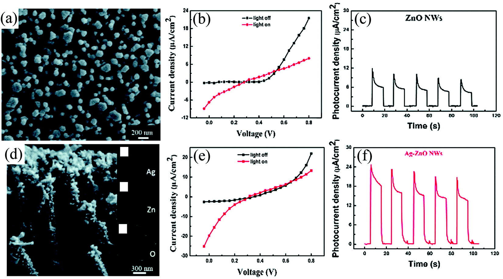 | ||
| Fig. 20 Microstructure of (a) ZnO NWs and (d) Ag–ZnO NWs along with the elemental mapping. The I–V characteristics of (b) ZnO NWs/H2O PD and (e) Ag–ZnO NWs/H2O PD under dark and UV (365 nm). The self-powered temporal (I–t) response of (c) ZnO NWs and (f) and Ag–ZnO NWs devices.121 [Reproduced with permission from ref. 121 from The Royal Society of Chemistry]. | ||
With this basic fundamental idea, various other works have also been done in this field by either playing around with the CE (replacing Pt),122 replacing the liquid electrolyte with a quasi-solid one84 and also modifying the photoanode by incorporating an additional HS with ZnO.85 Li et al., in their work,122 demonstrated a self-powered PECC type ZnO PD with Pt-free CE. The device consisted of ZnO NRs as the photoanode, [Co(bpy)3]2+/3+ as the electrolyte, and PEDOT/ITO as the CE. It showed improved performance with enhanced device response, as shown in Fig. 21(a) and (b). The PD with PEDOT/ITO as the CE depicted an open circuit voltage of 0.5 V and a short-circuit current of 6.2 µA with UV response times of <0.2 s. The self-powering mechanism of the device is depicted in Fig. 21(c). The reason behind the obtained enhanced response is the superior catalytic activity of PEDOT as compared to that of Pt.122 The next adopted approach toward designing a ZnO-based self-powered PECC type PD was presented by Peng et al., utilizing a quasi solid-state electrolyte.84 In their work, they used an iodine-free electrolyte containing 1-methyl-3-propylimidazolium iodide, potassium iodide (KI), and poly(ethylene oxide) (PEO). The photoanode was that of ZnO and the CE was that of Pt-FTO. In such a configuration, the device exhibited a high Ri of 2.33 AW−1 with tr and tf of 0.09 and 0.31 s, respectively. The device I–V under dark and with light illumination is depicted in Fig. 21(d), with the inset showing the magnified I–V without any illumination. The presence of the Schottky barrier is depicted in the I–V curves under both the conditions. The obtained photocurrent at zero-bias is 1.4 × 10⁻⁴ A, which is much larger than the dark current (2.62 × 10⁻⁷ A). Further, a stable (even after 4 months), repeatable, and rapid self-powering temporal response for varying amounts of KI is portrayed by the device, as shown in Fig. 21(e). The as-associated self-powering mechanism is depicted in Fig. 21(f).84
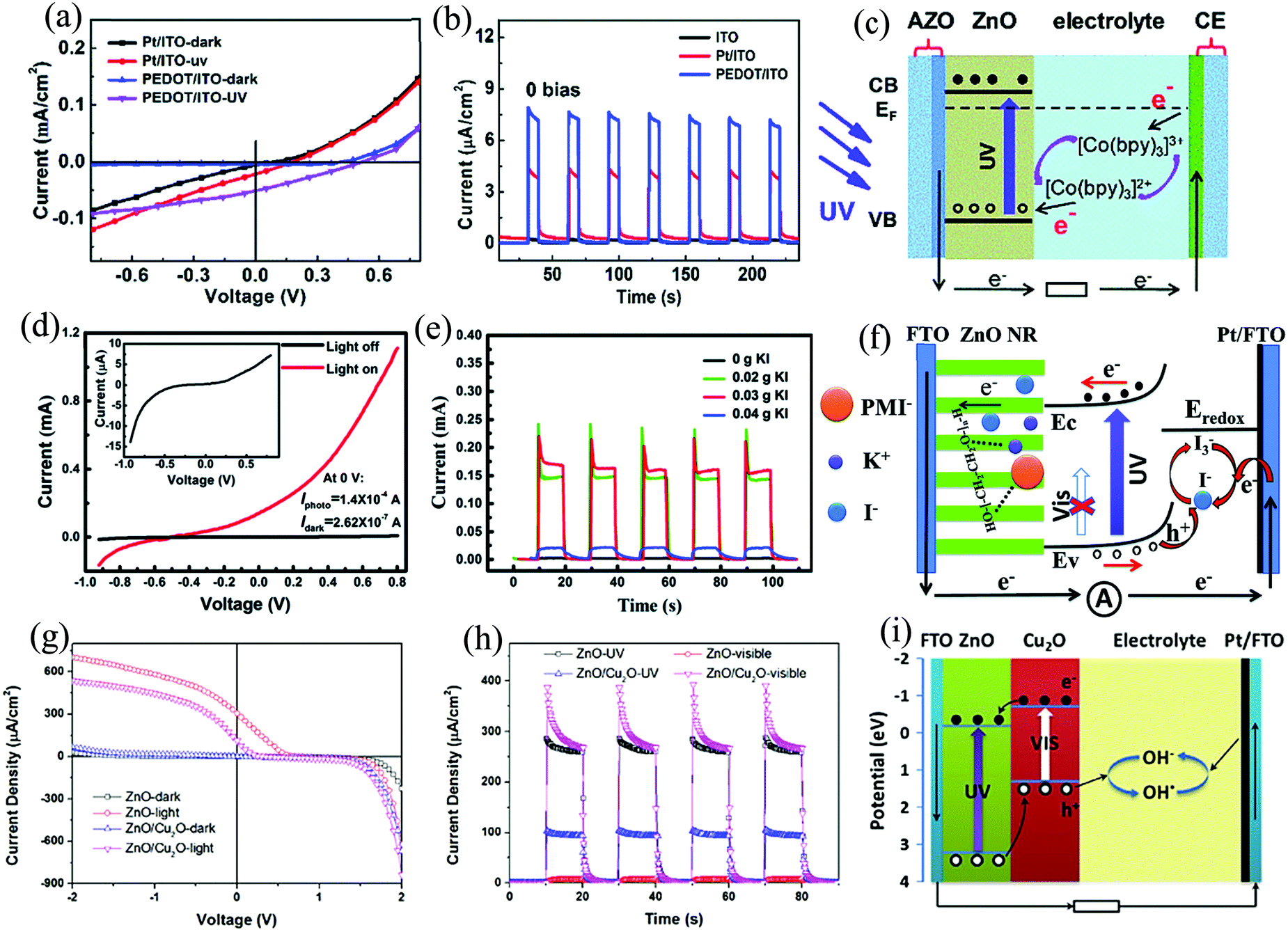 | ||
| Fig. 21 (a) I–V characteristics of ZnO NRs/[Co(bpy)3]2+/3+ PD under dark and UV (365 nm) with Pt/ITO and PEDOT/ITO CE. (b) Zero-bias I–t characteristics of ZnO NRs/[Co(bpy)3]2+/3+ under UV with ITO, Pt/ITO, and PEDOT/ITO CE. (c) Energy band diagram of the PD under UV.122 (d) I–V characteristics of ZnO NRs/quasi solid-state electrolyte PD under dark and UV (365 nm). (e) Zero-bias I–t characteristics of the ZnO NRs/quasi solid-state electrolyte PD. (f) Schematic for self-powering UV detection mechanism in the PD.84 (g) I–V characteristics of ZnO NWs/electrolyte and ZnO/Cu2O branched HS/electrolyte PD under dark and UV (355 nm). (h) Zero-bias I–t characteristics of these PDs under UV and visible (λ > 425 nm). (i) Schematic for self-powering UV and visible photodetection mechanism in the PD.85 [Reproduced with permissions from ref. 84 and 122 from The Royal Society of Chemistry and Reprinted from, J. Alloys Compd., Z. Bai and Y. Zhang, 675, 325–330,85 © 2016, with permission from Elsevier]. | ||
A third approach toward improving performance of these ZnO-based self-powered PECC-type PDs has been to add an additional heterojunction with ZnO. One of the benefits that this additional heterojunction can provide is to extend the range of spectral response. For e.g., Bai et al., in their work, used the HS of ZnO and Cu2O (Eg ∼ 2.0 eV) as the active photoanode, which provided sensitivity toward both the UV and visible radiation. Apart from extending the range of wavelength sensitivity, ZnO and Cu2O forms a type-II heterojunction, which further helps in the efficient separation of the photogenerated e−–h+ pairs. The complete device was fabricated using this HS as the photoanode, sodium sulphate (Na2SO4) as the electrolyte, and Pt/FTO as the CE. Rectifying the I–V characteristics of the device (with and without Cu2O) under dark and under UV (355 nm) is depicted in Fig. 21(g). Moreover, a highly stable and repeatable self-powering I–t response under UV and visible (λ > 425 nm) with respective tr and tf of 0.14 s and 0.36 s is presented by the device, as shown in Fig. 21(h). The energy band diagram of the PD for the detection of UV and visible light is depicted in Fig. 21(i).85
The intrinsic properties of ZnO such as piezoelectricity,123,124 pyroelectricity,125 and pyro-phototronic88,126 effects can also contribute synergistically to the performance of self-powered photodetection. Prof. Z.L. Wang and his group have an unmatched contribution toward exploring these different properties of ZnO NSs and demonstrating the applications in various fields of science and technology.127 In one of the work by Lin et al., they incorporated the concept of piezopolarization charges to enhance the self-powering response of a ZnO PECC PD.128 Upon application of 0.15% compressive strain, they could enhance the self-powered response by 48%. In their work, the photoanode was fabricated by the technique of radio-frequency magnetron sputtering by depositing ZnO film on a flexible ITO-poly(ethyleneterephthalate) (PET) substrate. The as-deposited film was then glued to a polystyrene (PS) cantilever with polydimethylsiloxane (Fig. 22(a)). The microstructure of the deposited film (cross-sectional) with the grain size varying in the range of 30–100 nm is depicted in Fig. 22(b), with the inset showing the top-view. The electrolyte used for the final device was Na2SO4.
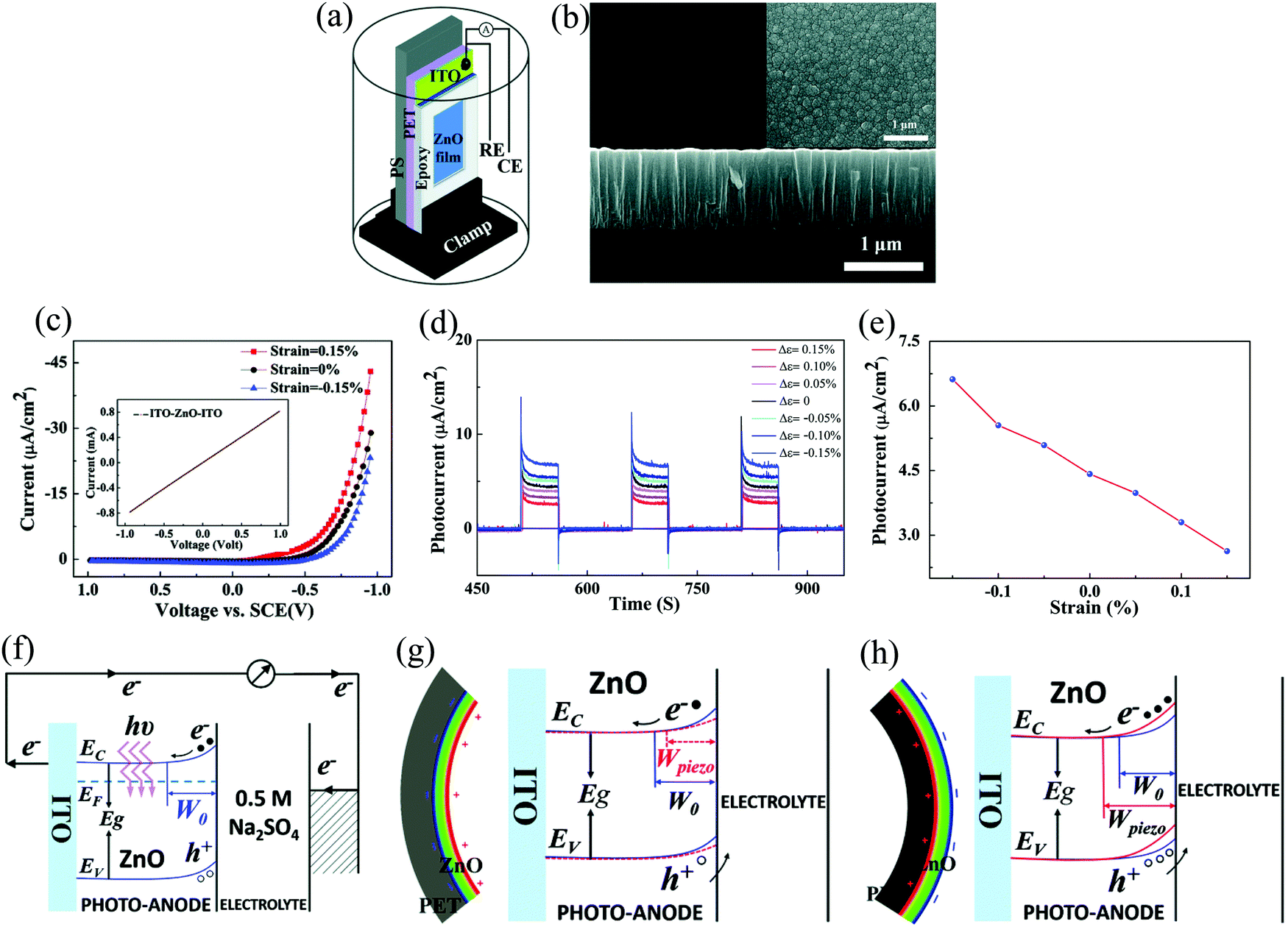 | ||
| Fig. 22 (a) Device schematic and (b) film cross-sectional SEM with the inset showing the top-view. (c) Dark I–V and (d) self-powering I–t (under illumination) characteristics of the PECC PD under the conditions of different applied strains. (e) Variation of the output photocurrent as a function of the applied strains. Energy band diagram of the device under (f) no strain, (g) tensile strain, and (h) compressive strain.128 [Reproduced with permission from ref. 128 from The Royal Society of Chemistry]. | ||
The I–V characteristics (Fig. 22(c)) depict the rectifying behavior arising from the bend bending (Schottky barrier) occurring at the interface of ZnO and Na2SO4. The origin of the rectifying nature is also further verified by measuring the I–V in the ITO–ZnO–ITO configuration (inset of Fig. 22(c)), which depicts an ohmic behavior. The I–Vs were further recorded in the presence of tensile and compressive strains of 0.15%, indicating a decrease/increase in the Schottky barrier height under tensile/compressive strains. The inherent built-in electric field was then explored for self-powering photoresponse under different strain conditions (Fig. 22(d)). From the experiments, it was observed that the photoresponse increased upon compressive strains while it decreased under the tensile one (Fig. 22(d) and (e)) with response times of the order of ∼ms. The underlying self-powering photoresponse mechanism under the conditions of strain and no strain are pictorially presented in Fig. 22(f)–(h). Fig. 22(f) depicts the interfacial band bending and the creation of space charge region, and thus the built-in electric field. Now, applying a tensile strain leads to the formation of permanent piezoelectric charges at the ZnO/Na2SO4 interface due to +c-orientation growth of the ZnO in the sputtered film. These positive piezopolarization charges lower the ZnO CB (Fig. 22(g)) by attracting the free e−s. The ultimate effect of this is reduction of the space-charge region, thus comparatively weakening the strength of the built-in electric field. Similarly, upon applying compressive strain, negative piezopolarization charges face the electrolyte side, thus depleting more e−s on the ZnO side and thus effectively increasing the space-charge region and the height of the Schottky barrier. This increase results in a comparatively enhanced built-in electric field (Fig. 22(h)) and thus more photocurrent by increasing the separation of the photogenerated charge carriers.128 This work by Lin et al.,128 provides another approach to tune the strength of the built-in electric field of the HS by utilizing the intrinsic material property of ZnO.
A tabular compilation of the various kinds of ZnO HS-based self-powered PDs is presented in Table 2.
| ZnO HS | Self-powering mechanism | Wavelength (nm) | Response/recovery time (s) | Responsivity(A W−1) | Specific detectivity/detectivity (Jones) |
|---|---|---|---|---|---|
| Gr/ZnO/Gr90 | Schottky-type | 365 | — | 540 × 10−6 | — |
| Gr/H-ZnO/AZO91 | Schottky-type | 365 | 32 × 10−3 | 50 × 10−6 | — |
| ZnO/GaN97 | Schottky-type | 350 | (731.6/53.1) × 10−3 | 95.8 × 10⁻³ | 2.9 × 10¹² |
| ZnO/ZnS98 | Schottky-type | 320–365 | 22.5/45 | 3.34 × 10⁻³ | 8.9 × 10¹² |
| 465–475 | — | — | — | ||
| 515–525 | 22.3/40 | 1.05 × 10⁻³ | 2.8 × 10¹² | ||
| 780–950 | 25.2/15 | 0.47 × 10⁻³ | 1.4 × 10¹² | ||
| ZnO/Au/Al2O3100 | Schottky-type | 365 | <0.16/<0.16 | 6.8 × 10⁻³ | 1.7 × 10⁹ |
| CD-Enhanced ZnO/graphite103 | Schottky-type | 330 | 2/3.2 | 9.5 × 10⁻³ | 4.27 × 10⁸ |
| n-ZnO/p-Cu2O104 | p–n junction type | 370–570 | 0.02/0.03 @370 nm | 0.24 @380 nm | — |
| 0.01/0.02 @450 nm | 0.06 @450 nm | — | |||
| n-ZnO/p-GaN81 | p–n junction type | 325 | (20/219) × 10−6 | 132 × 10−3 | — |
| n-GIZO/p-GaN108 | p–n junction type | 360–400 | 1.5/0.8 | 5.29 × 10⁻³ | 7.98 × 10⁹ |
| n-ZnO/CdS/p-GaN109 | p–i–n junction type | 300 | <0.35 | 176 × 10−3 | 2.5 × 10¹² |
| n-ZnO/p-NiO110 | p–n junction type | 355 | 0.23/0.21 (@∼0.1 mV) | 0.44 × 10⁻³ | — |
| n-ZnO/p-CuSCN111 | p–n junction type | 355/380 | 0.5/6.7 × 10−6 | 7.5 × 10⁻³ | — |
| n-ZnO/p-CuI112 | p–n junction type | 365 | 0.41/0.24 | 17.7 × 10⁻³ | 5 × 10⁹ |
| n-ZnO/p-CuI/Au112 | p–n junction type | 365 | 0.41/0.08 | 61.5 × 10⁻³ | 1.7 × 10¹⁰ |
| n-ZnO/p-Co3O4113 | p–n junction type | Visible | — | 1312.5 × 10−9 | — |
| n-ZnO/p-Te119 | p–n junction type | 300 | 2.46/1.75 | 387 × 10−3 | 4 × 10¹⁰ |
| n-Cl:ZnO/p-PEDOT:PSS88 | p–n junction type | 365 | (28/23) × 10−3 | 2.33 × 10⁻³ | 1.54 × 10¹⁰ |
| n-H:VZnO/p-PEDOT:PSS87 | p–n junction type | 365 | (23/26) × 10−3 | 2.65 × 10⁻³ | 5.25 × 10¹⁰ |
| n-ZnO/p-PANI120 | p–n junction type | 365 | 3.60/7.65 | 5.4 | — |
| ZnO/H2O/Pt-FTO121 | PECC type | 365 | 0.15/0.50 | 0.11 | — |
| Ag–ZnO/H2O/Pt-FTO121 | PECC type | 365 | 0.14/0.52 | 0.37 | — |
| ZnO/[Co(bpy)3]2+/3+/PEDOT-ITO122 | PECC type | 365 | <0.2/<0.2 | — | — |
| ZnO/quasi solid-state electrolyte/Pt-FTO84 | PECC type | 365 | 0.09/0.31 | 2.33 | — |
| ZnO–Cu2O/Na2SO4/Pt-FTO85 | PECC type | 355 | 0.14/0.36 s | 19.3 × 10⁻³ | — |
| λ > 425 | 0.14/0.36 s | 8.2 × 10⁻³ (@400 nm) | — |
Self-powered/charging zinc oxide heterostructure supercapacitor
One such example is the electric eel, also known as Electrophorus electricus, which is a known self-powered system with power generation from ionic gradients.134,135 It is capable of generating an electric discharge of 100 W using the ionic flux.136 In order to defend itself, the eel uses transient current spikes as the electric shock.134,137 In biological systems, the presence of highly selective and actuatable ion channels act as the source of electrical power by generating large voltages and currents (Fig. 23(a) and (b)).137–139 Electrochemical batteries and capacitors are close engineering examples of developing charge storage systems similar to most natural organisms. Recently, a large interest has arisen in developing electrochemical capacitors due to its high power-density compared to the batteries. Two leading mechanisms of charge storage in electrochemical capacitors are (1) electric double charge layer formation at the interface of the electrode and electrolyte, and some electrode materials along with faradaic charge contribution that are attributed to (2) pseudocapacitance. Among various existing materials, carbon-based56,140,141 and metal-oxide142,143 based SCs are being widely studied.143 Readers are encouraged to read the latest review by Miao et al.,140 for a comprehensive understanding on carbon-based SCs. Additional reviews by Wang et al.,144 and An et al.,145 are also suggested for an in-depth understanding on the field of SCs and the recent progresses made. ZnO, in addition to being an excellent optically sensitive material, can also be effectively used in an electroactive system such as SC146–148 due to the occurrence of redox reactions149,150 and increased surface-to-volume ratio,151 especially in the NRs. This high surface-to-volume ratio also help in hosting several electroactive systems, such as spinel nickel cobaltite (NiCo2O4).151 Further, as seen above in Prof. Misra's88 and Lin et al.'s128 work, the charge generation and separation in ZnO is not only controlled by light but is also a function of mechanical and thermal stimuli. A recent perspective by Pu and Wang152 on self-charging power systems, i.e., systems that simultaneously harvest and store energy, along with power management capabilities, have been elaborated in detail in their recent article.152 The intrinsic piezoelectricity of ZnO NRs/NWs thus helps in fabricating self-charging SC with ZnO NRs/NWs acting as the potential generator.153 Finally, coupling its optical sensitivity helps in developing opto-electrochemical systems with self-powered operation.154 A few examples of electrochemical capacitors are outlined in the following discussion that are developed for the self-charging operation. For the sake of simplicity and generality, these SCs will be classified based on their modes of operations, i.e., contact or non-contact. The contact mode refers to SCs that operate due to piezopolarization charges arising from physical stresses, while the non-contact ones refer to the ones that self-charge via an optical stimulus.
 | ||
| Fig. 23 (a) Image of Electrophorus electricus. Inset on the top depicts the electrocytes' arrangement within its electric organs while that at the bottom shows the ion fluxes in their firing state. (b) Voltage generation mechanism in the electrocytes.139 [Reprinted by permission from Springer Nature: Nature, T. B. H. Schroeder et al., 552, 214–218139 © 2017]. | ||
Contact mode
Ramadoss et al. fabricated a self-charging SC power cell (SCSPC) with poly(vinylidene difluoride) (PVDF)–ZnO as the separator (Fig. 24).153 | ||
| Fig. 24 (a) Schematic of SCSPC. (b) Voltage vs. time graph to depict the self-charging of the SCSPC by a human palm impact. (c) Step-wise working mechanism of the SCSPC.153 [Reprinted with permission from A. Ramadoss et al., ACS Nano, 9, 4337–4345,153 © 2015 American Chemical Society]. | ||
The SC electrodes consisted of manganese dioxide (MnO2) as the electroactive material mixed with carbon black and PVDF. The slurry of this mixture was then coated on aluminium foil and finally, the SCSPC was assembled by sandwiching PVA/H3PO4 with a separator. In this case, PVDF–ZnO plays a dual role, first as a separator and second as a potential generator (Fig. 24(a)). Mechanically deforming the device (on the top) creates a piezoelectric field (potential) in the PVDF–ZnO separator film. Under this condition of compressive strain, the as-fabricated SC could self-charge to ∼110 mV in 300 s (Fig. 24(b)). The generated piezoelectric field results in H+ ion migration through the separator (PVDF–ZnO) in the electrolyte to the negative electrode and consequently in charging reactions at the two electrodes. Upon releasing the compressive strain, a reverse reaction is observed, thus directing the ions to restore their original position (Fig. 24(c)). The system is interesting for developing a self-powered/charging system; however, the problem is that the piezoelectric separator hinders efficient ion transport and, moreover, this is also a contact method for self-charging.
Another attempt toward creating a self-charging power unit (SCPU) was made by Rasheed et al., in their work.155
The SCPU was fabricated using a composite matrix of ZnO NFs, rGO and PVDF as the piezo-separator film with MnO2–rGO as the active electrode material for the solid-state SC. The synthesis of rGO was carried out by modified Hummers’ method,155,156 MnO2 NWs by the hydrothermal method, and ZnO NFs via a two-step chemical route.155 For the MnO2 NWs synthesis, a solution mixture of KMnO4, DI water, (NH4)2S2O8, and HNO3 mixed/prepared under optimized conditions was transferred into an autoclave (Teflon-lined), and kept at 80 °C for 15 h. The MnO2 NWs was then finally obtained by cleaning, centrifugation, and drying at 80 °C for 10 h. For the SC electrode, (MnO2)–rGO HS was prepared by ultrasonication, followed by drying the HS solution in an oven at 60 °C. Later, the HS composite paste was mixed with PVDF and carbon black in a solution of N-methyl-2-pyrrolidone. Finally, the paste was drop-cast on Au-coated PET and dried at 70 °C for 4 h before use. Crystalline ZnO NFs (<10 nm) were synthesized using [Zn(CH3COO)2·2H2O] as the seed layer and later precipitating with NaOH.155 The polymer composite for the piezo-separator film was prepared by adding an appropriate amount of ZnO, rGO, and PVDF in dimethylformamide and mixing them under proper temperature conditions. After synthesis, the SCPU was fabricated by sandwiching poly(vinyl alcohol) (PVA)–H3PO4 solid electrolyte covered PVDF–ZnO–rGO film in between the MnO2–rGO HS symmetric electrode. The device schematic is presented in Fig. 25(a) with Au-coated PET as the current collectors. The self-charging behavior of a SCPU single unit is presented in Fig. 25(b). Upon applying a compressive force (using hand-tapping), the as-fabricated SCPU was able to store 1.5 × 10⁻³ mC of charge on its electrodes within 100 s, corresponding to the self-charging of ∼195–200 mV. Further, upon the removal of the compressive force, the SC unit stored the charges as the voltage was constant in the interval of 100–140 s (Fig. 25(b)). Fig. 25(c) schematically depicts the working mechanism of the SCPU governed by the redox reactions occurring due to the change in the electrode (MnO2–rGO) potential arising from the relaxation and compression of the piezo-separator (PVDF–ZnO–rGO) film. Upon applying a compressive force on the electrodes, the internal symmetry of the piezo-separator gets disturbed, thereby resulting in a piezoelectric potential generation across the separator thickness. This generated potential leads to potential distribution along the positive and negative sides, which in turn help in driving the electrolytic ions and thus storage the charge. The piezopotential leads to the development of H+ ion concentration gradient along the electrodes, contributing toward the electrochemical redox reactions and thus self-charging. On the removal of the applied force, the separator film comes at an equilibrium with a tiny number of ions that return to the electrolyte for compensation. With no further redox reaction occurring, only the electron transfer takes place.155 The main hurdle in this system is its contact mode of operation.
 | ||
| Fig. 25 (a) Schematic of SCPU. (b) Self-charging process of the SCPU under compressive force. (c) Sequential steps to depict the mechanical deformation-driven working mechanism of the SCPU.155 [Reprinted with permission from A. Rasheed et al., ACS Appl. Mater. Interfaces, 12, 20891–20900,155 © 2020 American Chemical Society]. | ||
Non-contact mode
An alternate route to this technology is utilizing the optical sensitivity of ZnO rather than the piezoelectricity, toward electrochemical performance. This route provides an alternative to contact mode self-charging by providing a non-contact route.157 The light interaction of ZnO to generate excitons can be used to enhance the contribution of self-generated electric double charge layer capacity in the electrochemical capacitor and thus, self-powered electrochemical capacitor.151Very recently, in 2020, Cortes et al. reported a photo-supercapacitor based on silver sulfide (Ag2S) QDs-decorated ZnO NRs.158 The NRs in this work were grown by the electrochemical method on FTO-covered glass. For the seed layer, an alcoholic solution of Zn(CH3COO)2 was spin coated and then dried (105 °C) and annealed (350 °C) under air. Thereafter, under appropriate conditions, electrodeposition for the growth of ZnO NRs was performed using the seed layer substrate as the working electrode. After the successful growth of the ZnO NRs, the Ag2S QDs were decorated using the technique of successive ionic layer adsorption and reaction, i.e., SILAR. In this technique, the NRs array was immersed successively in solutions containing Ag+ cations and S2− anions and later cleaned with alcohol for removing the excess weakly bound surface ions. After nine such SILAR, the decoration was completed with annealing (400 °C, 1 h) under N2 atmosphere.158 The surface of this NS was then passivated by ZnS using the same method of SILAR with Zn2+ cations and S2− anions. Finally, for h+ transportation, a layer of PEDOT was electrodeposited on the ZnS-passivated Ag2S QDs-decorated ZnO NRs. The process flow schematic of the nanocomposite synthesis is depicted in Fig. 26(a) with the corresponding microstructures in Fig. 26(b).
 | ||
| Fig. 26 (a) Diagrammatic representation of the nanocomposite synthesis. (b) Microstructure of (i) ZnO NRs, (ii) Ag2S QDs-decorated ZnO NRs, (iii) ZnS-passivated composite, and (iv) PEDOT-covered nanocomposite. (c) Photocharging and galvanostatic discharging behavior of the SC. (d) Energy band diagram to depict the mechanism of photocharging in the SC.158 [Reproduced with permission from ref. 158 from The Royal Society of Chemistry]. | ||
Fig. 26(c) shows the photocharging (under AM1.5G simulated sunlight of intensity 100 mW cm−2) and galvanostatic discharge behavior (under dark) of the SC for different current densities varying in the range of 4–400 µA cm−2. Upon illumination of light, the device gets photocharged to 330 mV in 40 s, after which it retains the same for 600 s. After charging, the device was discharged galvanostatically with different current densities. For a current density of 4 µA cm−2, the discharge time was 55 s (Fig. 26(c)) and the same was 2 s and 1 s for 40 µA cm−2 (blue line) and 400 µA cm−2 (red line), respectively (inset of Fig. 26(c)). The working mechanism of this photosupercapacitor is shown in Fig. 26(d). Under light illumination, the photo-excited electrons in the QDs (Eg ∼ 1.1 eV) transfer to the ZnO NRs, which get accumulated in the PEDOT CE to effectively accumulate the negative charges. At the same instant, the h+s get transported to PEDOT, thus accumulating positive charges. These accumulated charges result in the movement of charges with BF4− toward the anode and [HemIm]+ to the cathode to form a double layer. In addition, there is also the oxidation and reduction of the perchlorate anion (ClO4−, from the PEDOT layer) (Fig. 26(d)). This effective nanocomposite thus results in a self-powered SC with the stimulus of light.
Further interesting works have also been reported in this domain by Prof. Misra's group, for e.g., by coating NiCo2O4 on ZnO NRs (Fig. 27(a)–(d)) via a hydrothermal route using nickel nitrate hexahydrate, cobalt nitrate hexahydrate, and urea in a solution medium of water with ethanol. The coating of NiCo2O4 on the ZnO NRs provided a higher surface area and, in addition, improved the movement of the e−s and ions. The other advantage is that the coupled system is also sensitive to UV, which provides photoinduced capacitive response. Upon comparison of the electrochemical performances of each device architecture (pristine ZnO NRs//ZnO NRs, NiCo2O4//NiCo2O4, and NiCo2O4/ZnO NRs//NiCo2O4/ZnO NRs SCs, Fig. 27(e)) it was observed that the NiCo2O4/ZnO NRs//NiCo2O4/ZnO NRs SC depicted the highest response. The area under the CV curve after UV illumination increases ∼2 times, thus providing higher capacitive response (Fig. 27(f)). This increase in the CV is attributed to an increase in the generated charge carriers due to UV.151
 | ||
| Fig. 27 SEM image of (a) ZnO NRs with the cross-sectional view depicted in the inset and (b) NiCo2O4-coated ZnO NRs. Inset in (b) depicts the energy dispersive X-ray analysis spectrum of NiCo2O4/ZnO NRs. (c) and (d) are the TEM and HRTEM images of NiCo2O4/ZnO NR. (e) CV response comparison of pristine ZnO NRs//ZnO NRs, NiCo2O4//NiCo2O4, and NiCo2O4/ZnO NRs//NiCo2O4/ZnO NRs SCs. (f) CV curves and (g) diagrammatic working mechanism illustration of NiCo2O4/ZnO NRs//NiCo2O4/ZnO NRs SC in the absence and presence of UV irradiation.151 [Reprinted by permission from John Wiley and Sons: Energy Technol. (Electronic), B. D. Boruah and A. Misra, 5, 1356–1363151 © 2017]. | ||
The working mechanism of this self-powered SC is depicted in Fig. 27(g), where, in addition to the external electric field, the generated internal field (in presence of UV) results in increased capacitive response.151 Furthermore, the boost to the capacitive response is also provided by the increased electrode conductivity and the participation of the photogenerated charge carriers in the faradaic redox reaction upon UV illumination.151
To extend the range of wavelength sensitivity, Prof. Misra's group extended their work further by coating ZnCo2O4 on hydrogenated ZnO NRs (ZCZO) (Fig. 28(a)).
 | ||
| Fig. 28 (a) ZCZO NRs PD diagrammatic presentation. (b) I–V characteristics of the PD both in the absence and presence of light illumination (UV and green) (inset presents the zoomed-in I–V in the range from −0.4 to 0.4 V). (c) Device operation schematic showing the SC connected with the PD in series and (d) photographic image of the same. (e) SC-powered temporal characteristics of the fabricated PD (ZnCo2O4/H:ZnO NRs) in the presence of light (UV and green light).61 [Reproduced with permission from ref. 61 from The Royal Society of Chemistry]. | ||
Hydrogenation was performed to improve the NRs conductivity.61 The I–V characteristics (both under dark and illumination) was linear for the ZCZO device, suggesting an ohmic behavior with the Ag contacts (Fig. 28(b)). The hybrid material was sensitive to both UV and visible radiation with increased current upon illumination.61 However, in contrast to previous observations, there was no zero-voltage offset for the device under the illumination condition (inset of Fig. 28(b)). The as-fabricated photodetector thus required an externally applied bias, which in this case was provided by an SC with one electrode as that of the hybrid material (Fig. 28(c) and (d)). With the SC as the powering source (providing voltage), the I–t characteristics were recorded, which depicted a stable cyclic response for both the wavelengths under a series connection with the SC (Fig. 28(e)). This study thus revealed a very important outcome with a single material performing both the optical and electrochemical sensitivity, and finally acting as a single unit with the PD being driven by its corresponding SC.61
The further motivation of this finding pushed Prof. Misra's group to develop a compact system of optically-driven self-powered SC. Thereby, in the forthcoming study, an opto-electrochemical system was fabricated and studied using ZCZO as the active material.154
The HS was grown hydrothermally on ITO-coated glass, which played the dual role of a transparent electrode as well as assisted in the generation of built-in electric field for the self-powering response. The microstructure of both ZnO and ZCZO reveals vertically-aligned NRs with the diameter and height of about 80–150 nm and 1.5 µm, and 150–500 nm and 5 µm, respectively (Fig. 29(a) and (b)). Upon UV illumination, a self-charging (under application of zero-bias) voltage of 350 mV was generated in the SC due to UV (Fig. 29(c)). The as-obtained self-powering voltage in this non-contact mode is ∼3.2 times higher compared to that obtained by Ramadoss et al.153 in the contact mode. From the electrochemical characteristics, an asymmetric CV profile was observed with the area under the CV being increased by ∼52% after UV illumination as compared to that under no illumination (Fig. 29(d)). Such an asymmetric profile could be accredited to the reactions occurring on the surface of positive electrode and the electrical double layer reactions on the negative electrode.154 Further, in response to UV light, the measured areal capacitance and the energy density were 150 µF cm−2 and 11.8 × 10⁻³ µW h cm−2 (∼3 times higher than in the absence of UV), respectively. The associated self-charging mechanism and thus the voltage generation under UV is elucidated vividly in Fig. 29(e). The respective band positions of ITO, ZnO, and ZnCo2O4 result in an effective separation of the generated e−s and h+s, thereby creating a built-in electric field. These free e−s and h+s then participate in the driving process of the cations and anions, thereby helping in charge storage. In addition, the photogenerated charges also effectively increase the conductivity of the electrode material, thereby increasing the electron transportation efficiency.154Table 3 summarizes the parameters relevant to the ZnO-based SC, which is attributed to the self-powering/charging capability. So far, the area of developing self-powered/charging SC has not been extensively exploited; however, a deep understanding of the ZnO-based interface engineering would allow to establish a novel paradigm in the field of renewable energy storage systems.
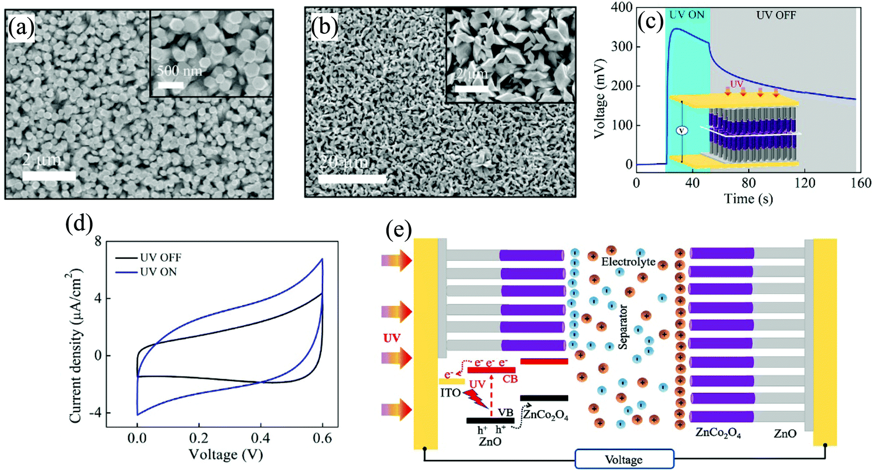 | ||
| Fig. 29 (a) Respective microstructure of (a) ZnO and (b) ZCZO NRs at low magnification and insets are at high magnification. (c) Self-charging response of the ZCZO SC under UV light and consequent discharging upon switching off the UV (inset depicting the device schematic). (d) CV comparison in both the absence and presence of UV (scan rate of 20 mV s−1). (e) Solid-state SC working mechanism under UV illumination.154 [Reprinted with permission from B. D. Boruah and A. Misra, ACS Appl. Energy Mater., 2, 278–286,154 © 2018 American Chemical Society]. | ||
| Supercapacitor | Role of ZnO | Mode of operation | Self-generated voltage (mV) | Capacitance |
|---|---|---|---|---|
| (PVDF)–ZnO153 | Separator | Contact | 110 @300 s | 455 mF g−1 @0.04 mA cm−2 |
| (PVDF–ZnO–rGO)155 | Separator | Contact | ∼195–200 @100 s | 7.6 F g−1 @25 mV s−1 |
| Ag2S QDs@ZnO NRs158 | Electrode | Non-contact | 330 @40 s | 0.667 mF cm−2 |
| NiCo2O4/ZnO NRs151 | Electrode | Non-contact | — | ∼24.4 mF g−1 @0.59 mA g−1 |
| ZCZO NRs61 | Electrode | Non-contact | — | 37 mF cm−2 @2.5 mA cm−2 |
| 13.8 F g−1 @1 A g−1 | ||||
| ZCZO NRs154 | Electrode | Non-contact | 350 mV @∼10 s | ∼236.6 µF cm−2@1.24 µA cm−2 |
Conclusion
In summary, HSs form an integral part of the semiconductor industry and have led to discoveries and studies contributing to the field of fundamental, applied, and technological sciences. The material of focus in this review, i.e., ZnO, is a versatile semiconductor that can be used to harvest both optical as well as electrochemical energy. In addition, its intrinsic n-type behavior and piezoelectricity favor energy conversion and harvesting in the absence of any external stimuli. The overall result is miniaturized self-charged and self-powered devices. The capability of ZnO to interface with other metallic and semiconducting materials provides wide range of possibilities for interface engineering focused on specific applications and device functionalities. A large Eg in ZnO facilitates the electronic connection with widely variable semiconductor interfaces for the broadband, selectively high responsivity to specific wavelengths, and ultrahigh response from the atomically small HSs. The clectrochemical response from the Zn-based interfaces through the optically-active device provided voltage generation to facilitate the ion movements across the electrodes. In the current scenario, the understanding of ZnO-based heterointerfaces can play a crucial role in printed large-scale wearable devices, qubits for quantum computing, development of novel on-chip platform for multifunctional devices, etc. ZnO properties further lead to the establishment of a novel paradigm in the field of self-powered energy storage. The compilation of studies on both PD and SC further provides a deep insight into the resultant charge carrier dynamics with exciton generation for the self-powering capability of various devices.Conflicts of interest
There are no conflicts to declare.References
- Z. L. Wang, Zinc oxide nanostructures: growth, properties and applications, J. Phys.: Condens. Matter, 2004, 16, R829–R858 CrossRef CAS
.
-
V. A. Coleman and C. Jagadish, Basic Properties and Applications of ZnO, Elesvier, 2006, pp. 1–20 Search PubMed
- P. A. Rodnyi and I. V. Khodyuk, Optical and Luminescence Properties of Zinc Oxide, Opt. Spectrosc., 2011, 111, 776–785 CrossRef CAS
- A. Janotti and C. G. Van de Walle, Fundamentals of zinc oxide as a semiconductor, Rep. Prog. Phys., 2009, 72, 126501 CrossRef
-
H. Morkoç and Ü. Özgür, Zinc Oxide: Fundamentals, Materials and Device Technology, Wiley-VCH Verlag GmbH & Co. KGaA, Weinheim, 2009, pp. 1–76 Search PubMed
- A. Kolodziejczak-Radzimska and T. Jesionowski, Zinc oxide—from synthesis to application: a review, Materials, 2014, 7, 2833–2881 CrossRef CAS PubMed
- S. J. Pearton, D. P. Norton, K. Ip, Y. W. Heo and T. Steiner, Recent progress in processing and properties of ZnO, Superlattices Microstruct., 2003, 34, 3–32 CrossRef CAS
- D. C. Look, B. Claflin, Y. I. Alivov and S. J. Park, Phys. Status Solidi A, 2004, 201, 2203–2212 CrossRef CAS
- A. Janotti and C. G. Van De Walle, Native point defects in ZnO, Phys. Rev. B: Condens. Matter Mater. Phys., 2007, 76, 165202 CrossRef
- A. A. Lotin, O. A. Novodvorsky, V. Y. Panchenko, L. S. Parshina, E. V. Khaydukov, D. A. Zuev, V. V. Rocheva, O. D. Khramova and K. D. Chtcherbachev, Ternary alloys CdyZn1−y O and MgxZn1−xO as materials for optoelectronics, Phys. Solid State, 2011, 53, 467–471 CrossRef CAS
- S. U. Awan, S. K. Hasanain, G. Hassnain Jaffari, D. H. Anjum and U. S. Qurashi, J, Defects induced luminescence and tuning of bandgap energy narrowing in ZnO nanoparticles doped with Li ions, J. Appl. Phys., 2014, 116, 083510 CrossRef
- Z. Ma, F. Ren, X. Ming, Y. Long and A. Volinsky, Cu-Doped ZnO electronic structure and optical properties studied by first-principles calculations and experiments, Materials, 2019, 12, 196 CrossRef CAS PubMed
- A. Shah, M. Ahmad, Rahmanuddin, S. Khan, U. Aziz, Z. Ali, A. Khan and A. Mahmood, The role of Al doping on ZnO nanowire evolution and optical band gap tuning, Appl. Phys. A: Mater. Sci. Process., 2019, 125, 1–8 CrossRef CAS
- T. L. Tan, C. W. Lai and S. B. Abd Hamid, Tunable band gap energy of Mn-doped ZnO nanoparticles using the co-precipitation technique, J. Nanomater., 2014, 2014, 371720 Search PubMed
- D. P. Joseph and C. Venkateswaran, Bandgap engineering in ZnO by doping with 3d transition metal ions, J. At. Mol. Opt. Phys., 2011, 2011, 270540 Search PubMed
-
C. Bundesmann, R. Schmidt-Grund and M. Schubert, Optical Properties of ZnO and Related Compounds, Springer, Berlin, Heidelberg, 2008, pp. 79–124 Search PubMed
-
A. Waag, Electrical Conductivity and Doping, Zinc Oxide. Springer Series in Materials Science, Springer, Berlin, Heidelberg, 2010, vol. 120, pp. 95–119 Search PubMed
- E. Schlenker, A. Bakin, T. Weimann, P. Hinze, D. H. Weber, A. Gölzhäuser, H. H. Wehmann and A. Waag, On the difficulties in characterizing ZnO nanowires, Nanotechnology, 2008, 19, 365707 CrossRef CAS PubMed
- A. D. Corso, M. Posternak, R. Resta and A. Baldereschi, Ab initio study of piezoelectricity and spontaneous polarization in ZnO, Phys. Rev. B: Condens. Matter Mater. Phys., 1994, 50, 10715–10721 CrossRef PubMed
- R. Wahab, F. Khan, Y. B. Yang, I. H. Hwang, H.-S. Shin, J. Ahmad, S. Dwivedi, S. T. Khan, M. A. Siddiqui, Q. Saquib, J. Musarrat, A. A. Al-Khedhairy, Y. K. Mishra and B. A. Ali, Zinc oxide quantum dots: multifunctional candidates for arresting C2C12 cancer cells and their role towards caspase 3 and 7 genes, RSC Adv., 2016, 6, 26111–26120 RSC
- S. Nandi, B. D. Boruah and A. Misra, Zinc oxide quantum dots decorated carbon nanotubes for improved opto-electro-mechanical response, Sens. Actuators, A, 2017, 267, 351–359 CrossRef CAS
- J. B. Cui, Zinc oxide nanowire, Mater. Charact., 2012, 64, 43–52 CrossRef CAS
- S. Mehra, E. M. Chan and A. Salleo, Modular synthetic design enables precise control of shape and doping in colloidal zinc oxide nanorods, J. Mater. Chem. C, 2015, 3, 7172–7179 RSC
- D. Jian, J.-J. Lai, Y.-F. Lin, J. Zhai, I. L. Li, F. Tian, S. Wang, P. Hua, M.-M. Ku, W.-B. Jian, S. Ruan and Z. Tank, Electron hopping transport in 2D zinc oxide nanoflakes, 2D Mater., 2017, 4, 025028 CrossRef
-
W. R. Frensley, Chapter 1-heterostructure and quantum well physics, in VLSI Electronics Microstructure Science, ed. N. G. Einspruch and W. R. Frensley, Elsevier, 1994, vol. 24, pp. 1–24 Search PubMed
-
B. L. Sharma and R. K. Purohit, Semiconductor Heterojunctions, Pergamon Press, Oxford, 1974 Search PubMed
- Y. Mogulkoc, M. Modarresi, A. Mogulkoc and B. Alkan, Electronic and optical properties of boron phosphide/blue phosphorus heterostructures, Phys. Chem. Chem. Phys., 2018, 20, 12053–12060 RSC
- N. Wang, D. Cao, J. Wang, P. Liang, X. Chen and H. Shu, Interface effect on electronic and optical properties of antimonene/GaAs van der Waals heterostructures, J. Mater. Chem. C, 2017, 5, 9687–9693 RSC
- X. Chen, Q. Yang, R. Meng, J. Jiang, Q. Liang, C. Tan and X. Sun, The electronic and optical properties of novel germanene and antimonene heterostructures, J. Mater. Chem. C, 2016, 4, 5434–5441 RSC
- J. Schrier, D. O. Demchenko, L.-W. Wang and A. P. Alivisatos, Optical properties of ZnO/ZnS and ZnO/ZnTe heterostructures for photovoltaic applications, Nano Lett., 2007, 7, 2377–2382 CrossRef CAS PubMed
- S. P. Singh, Z. E. Ooi, S. N. L. Geok, G. K. L. Goh and A. Dodabalapur, Electrical characteristics of zinc oxide-organic semiconductor lateral heterostructure based hybrid field-effect bipolar transistors, Appl. Phys. Lett., 2011, 98, 31 Search PubMed
- J. Tersoff, Theory of semiconductor heterojunctions: The role of quantum dipoles, Phys. Rev. B: Condens. Matter Mater. Phys., 1984, 30, 4874–4877 CrossRef CAS
- K. Xu, Y. Gu, C. Song, X. Zhong and J. Zhu, Atomic insight into spin, charge and lattice modulations at SrFeO3− x/SrTiO3 interfaces, Nanoscale, 2021, 13, 6066–6075 RSC
- C. L. Prajapat, S. Singh, A. Paul, D. Bhattacharya, M. R. Singh, S. Mattauch, G. Ravikumar and S. Basu, Superconductivity-induced magnetization depletion in a ferromagnet through an insulator in a ferromagnet–insulator–superconductor hybrid oxide heterostructure, Nanoscale, 2016, 8, 10188–10197 RSC
- J. A. Sulpizio, S. Ilani, P. Irvin and J. Levy, Nanoscale phenomena in oxide heterostructures, Annu. Rev. Mater. Res., 2014, 44, 117–149 CrossRef CAS
- P. Zubko, S. Gariglio, M. Gabay, P. Ghosez and J.-M. Triscone, Interface physics in complex oxide heterostructures, Annu. Rev. Condens. Matter Phys., 2011, 2, 141–165 CrossRef CAS
- J. H. Ngai, F. J. Walker and C. H. Ahn, Correlated oxide physics and electronics, Annu. Rev. Mater. Res., 2014, 44, 1–17 CrossRef CAS
- A. Ohtomo and H. Y. Hwang, A high-mobility electron gas at the LaAlO3/SrTiO3 heterointerface, Nature, 2004, 427, 423–427 CrossRef CAS PubMed
- S. Thiel, G. Hammerl, A. Schmehl, C. W. Schneider and J. Mannhart, Tunable quasi-two-dimensional electron gases in oxide heterostructures, Science, 2006, 313, 1942–1945 CrossRef CAS PubMed
- N. Reyren, S. Thiel, A. Caviglia, L. FittingKourkoutis, G. Hammerl, C. Richter, C. W. Schneider, T. Kopp, A.-S. Rüetschi, D. Jaccard, M. Gabay, D. A. Muller, J.-M. Triscone and J. Mannhart, Superconducting interfaces between insulating oxides, Science, 2007, 317, 1196–1199 CrossRef CAS PubMed
- A. Gozar, G. Logvenov, L. F. Kourkoutis, A. T. Bollinger, L. A. Giannuzzi, D. A. Muller and I. Bozovic, High-temperature interface superconductivity between metallic and insulating copper oxides, Nature, 2008, 455, 782–785 CrossRef CAS PubMed
- E. Bousquet, M. Dawber, N. Stucki, C. Lichtensteiger, P. Hermet, S. Gariglio, J. Triscone and P. Ghosez, Improper ferroelectricity in perovskite oxide artificial superlattices, Nature, 2008, 452, 732–736 CrossRef CAS PubMed
- T. Koida, M. Lippmaa, T. Fukumura, K. Itaka, Y. Matsumoto, M. Kawasaki and H. Koinuma, Effect of A-site cation ordering on the magnetoelectric properties in [(LaMnO3)m/(SrMnO3)m]n artificial superlattices, Phys. Rev. B: Condens. Matter Mater. Phys., 2002, 66, 144418 CrossRef
- A. M. Haghiri-Gosnet and J. P. Renard, CMR manganites: physics, thin films and devices, J. Phys. D: Appl. Phys., 2003, 36, R127–R150 CrossRef CAS
- S. Gbadamasi, M. Mohiuddin, V. Krishnamurthi, R. Verma, M. W. Khan, S. Pathak, K. Kalantar-Zadeh and N. Mahmood, Interface chemistry of two-dimensional heterostructures – fundamentals to applications, Chem. Soc. Rev., 2021, 50, 4684–4729 RSC
- H. Wang, L. Zhang, Z. Chen, J. Hu, S. Li, Z. Wang, J. Liu and X. Wang, Semiconductor heterojunction photocatalysts: design, construction, and photocatalytic performances, Chem. Soc. Rev., 2014, 43, 5234–5244 RSC
- R. Zhang, W. Jian, Z. Di Yang and F. Q. Bai, Insights into the photocatalytic mechanism of the C4N/MoS2 heterostructure: A first-principle study, Chin. Chem. Lett., 2020, 31, 2319–2324 CrossRef CAS
- H. Wang, X. Yuan, H. Wang, X. Chen, Z. Wu, L. Jiang, W. Xiong, Y. Zhang and G. Zeng, One-step calcination method for synthesis of mesoporous gC3N4/NiTiO3 heterostructure photocatalyst with improved visible light photoactivity, RSC Adv., 2015, 5, 95643–95648 RSC
- Y. Song, K. Xia, Y. Gong, H. Chen, L. Li, J. Yi, X. She, Z. Chen, J. Wu, H. Li and H. Xu, Controllable synthesized heterostructure photocatalyst Mo2C@C/2D g-C3N4: enhanced catalytic performance for hydrogen production, Dalton Trans., 2018, 47, 14706–14712 RSC
- R. Tripathi, P. Bhattacharyya, S. Nandi, A. Shukla and A. Misra, Molecular switching operation in gate constricted interface of MoS2 and hBN heterostructure, Appl. Mater. Today, 2021, 23, 100999 CrossRef
- Z. I. Alferov, The history and future of semiconductor heterostructures from the point of view of a Russian scientist, Phys. Scr., 1996, T68, 32–45 CrossRef CAS
- C. Weisbuch, The future of physics
of heterostructures: a glance into the crystal (quantum) ball, Phys. Scr., 1996, T68, 102–112 CrossRef CAS
- L. L. Chang and L. Esaki, Semiconductor quantum heterostructures, Phys. Today, 1992, 45, 36–43 CrossRef CAS
- H. Kroemer, Heterostructure devices: A device physicist looks at interfaces, Surf. Sci., 1983, 132, 543–576 CrossRef CAS
- S. Nandi and A. Misra, Spray coating of two-dimensional suspended film of vanadium oxide-coated carbon nanotubes for fabrication of a large volume infrared bolometer, ACS Appl. Mater. Interfaces, 2020, 12, 1315–1321 CrossRef CAS PubMed
- B. D. Boruah, S. Nandi and A. Misra, Layered assembly of reduced graphene oxide and vanadium oxide heterostructure supercapacitor electrodes with larger surface area for efficient energy-storage performance, ACS Appl. Energy Mater., 2018, 1, 1567–1574 CrossRef CAS
- Z. I. Alferov, H. Kroemer and J. S. Kilby, Nobel Prize in Physics 2000. Available online: https://www.nobelprize.org/prizes/physics/2000/summary/.
- P. Bhatnagar, T. T. Nguyen, S. Kim, J. H. Seo, M. Patel and J. Kim, Transparent photovoltaic memory for neuromorphic device, Nanoscale, 2021, 13, 5243–5250 RSC
- A. Kaphle, E. Echeverria, D. N. Mcllroy and P. Hari, Enhancement in the performance of nanostructured CuO–ZnO solar cells by band alignment, RSC Adv., 2020, 10, 7839–7854 RSC
- M. T. Uddin, M. E. Hoque and M. Chandra Bhoumick, Facile one-pot synthesis of heterostructure SnO2/ZnO photocatalyst for enhanced photocatalytic degradation of organic dye, RSC Adv., 2020, 10, 23554–23565 RSC
- B. Deka Boruah, A. Maji and A. Misra, Synergistic effect in the heterostructure of ZnCo2O4 and hydrogenated zinc oxide nanorods for high capacitive response, Nanoscale, 2017, 9, 9411–9420 RSC
- S. Wang, C. Ren, H. Tian, J. Yu and M. Sun, MoS2/ZnO van der Waals heterostructure as a high-efficiency water splitting photocatalyst: a first-principles study, Phys. Chem. Chem. Phys., 2018, 20, 13394–13399 RSC
- S. Wang, H. Tian, C. Ren, J. Yu and M. Sun, Electronic and optical properties of heterostructures based on transition metal dichalcogenides and graphene-like zinc oxide, Sci. Rep., 2018, 8, 1–6 Search PubMed
- M. Xu, X. Li, C. Jin, Z. He, X. Zhang and Q. Zhang, Novel and dual-mode strain-detecting performance based on a layered NiO/ZnO p–n junction for flexible electronics, J. Mater. Chem. C, 2020, 8, 1466–1474 RSC
- J. Song, H. Zheng, M. Liu, G. Zhang, D. Ling and D. Wei, A first-principles study on the electronic and optical properties of a type-II C2N/g-ZnO van der Waals heterostructure, Phys. Chem. Chem. Phys., 2021, 23, 3963–3973 RSC
- H. Zeng, Y. Cao, J. Yang, Z. Tang, X. Wang and L. Sun, Synthesis, optical and electrochemical properties of ZnO nanowires/graphene oxide heterostructures, Nanoscale Res. Lett., 2013, 8, 133–139 CrossRef PubMed
- Z. Li, X. Meng and Z. Zhang, Recent development on MoS2-based photocatalysis: A review, J. Photochem. Photobiol., C, 2018, 35, 39–55 CrossRef CAS
- H. L. Zhuang and R. G. Hennig, Computational search for single-layer transition-metal dichalcogenide photocatalysts, J. Phys. Chem. C, 2013, 117, 20440–20445 CrossRef CAS
- M. T. L. Lai, K. M. Lee, T. C. K. Yang, G. T. Pan, C. W. Lai, C.-Y. Chen, M. R. Johan and J. C. Juan, The improved photocatalytic activity of highly expanded MoS2 under visible light emitting diodes, Nanoscale Adv., 2021, 3, 1106–1120 RSC
- S. Sun, X. Li, W. Wang, L. Zhang and X. Sun, Photocatalytic robust solar energy reduction of dinitrogen to ammonia on ultrathin MoS2, Appl. Catal., B, 2017, 200, 323–329 CrossRef CAS
- W. Tian, Y. Wang, L. Chen and L. Li, Self-Powered Nanoscale Photodetectors, Small, 2017, 13, 1701848 CrossRef PubMed
- H. Qiao, Z. Huang, X. Ren, S. Liu, Y. Zhang, X. Qi and H. Zhang, Self-powered photodetectors based on 2D materials, Adv. Opt. Mater., 2020, 8, 1900765 CrossRef CAS
- Z. L. Wang, Towards self-powered nanosystems: from nanogenerators to nanopiezotronics, Adv. Funct. Mater., 2008, 18, 3553–3567 CrossRef CAS
- X. Hu, X. Li, G. Li, T. Ji, F. Ai, J. Wu, E. Ha and J. Hu, Recent Progress of Methods to Enhance Photovoltaic Effect for Self-Powered Heterojunction Photodetectors and Their Applications in Inorganic Low-Dimensional Structures, Adv. Funct. Mater., 2021, 2011284 CrossRef CAS
- X. Li, X. Liu, Y. Li, D. Gao and L. Cao, Using Novel Semiconductor Features to Construct Advanced ZnO Nanowires-based Ultraviolet Photodetectors: A Brief Review, IEEE Access, 2021, 9, 11954–11973 Search PubMed
- Z. L. Wang, J. Chen and L. Lin, Progress in triboelectric nanogenerators as a new energy technology and self-powered sensors, Energy Environ. Sci., 2015, 8, 2250–2282 RSC
- D. Periyanagounder, P. Gnanasekar, P. Varadhan, J.-H. He and J. Kulandaivel, High performance, self-powered photodetectors based on a graphene/silicon Schottky junction diode, J. Mater. Chem. C, 2018, 6, 9545–9551 RSC
- L.-B. Luo, H. Hu, X.-H. Wang, R. Lu, Y.-F. Zou, Y.-Q. Yu and F.-X. Liang, A graphene/GaAs near-infrared photodetector enabled by interfacial passivation with fast response and high sensitivity, J. Mater. Chem. C, 2015, 3, 4723–4728 RSC
- L.-B. Luo, J.-J. Chen, M.-Z. Wang, H. Hu, C.-Y. Wu, Q. Li, L. Wang, J.-A. Huang and F.-X. Liang, Near-infrared light photovoltaic detector based on GaAs nanocone array/monolayer graphene Schottky junction, Adv. Funct. Mater., 2014, 24, 2794–2800 CrossRef CAS
- U. Y. Won, B. H. Lee, Y. R. Kim, W. T. Kang, I. Lee, J. E. Kim, Y. H. Lee and W. J. Yu, Efficient photovoltaic effect in graphene/h-BN/ silicon heterostructure self-powered photodetector, Nano Res., 2021, 14, 1967–1972 CrossRef CAS
- Y. Q. Bie, Z. M. Liao, H. Z. Zhang, G. R. Li, Y. Ye, Y. B. Zhou, J. Xu, Z. X. Qin, L. Dai and D. P. Yu, Self-powered, ultrafast, visible-blind UV detection and optical logical operation based on ZnO/GaN nanoscale p-n junctions, Adv. Mater., 2011, 23, 649–653 CrossRef CAS PubMed
- Y. Zhu, K. Liu, Q. Ai, Q. Hou, X. Chen, Z. Zhang, X. Xie, B. Li and D. Shen, A high performance self-powered ultraviolet photodetector based on a p-GaN/n-ZnMgO heterojunction, J. Mater. Chem. C, 2020, 8, 2719–2724 RSC
- Q. Li, L. Wei, Y. Xie, K. Zhang, L. Liu, D. Zhu, J. Jiao, Y. Chen, S. Yan, G. Liu and L. Mei, ZnO nanoneedle/H2O solid-liquid heterojunctionbased self-powered ultraviolet detector, Nanoscale Res. Lett., 2013, 8, 1–7 CrossRef PubMed
- X. Peng, Y. Zeng, X. Pan, W. Wang, Y. Zhou, F. Wang, Q. Lu and Z. Ye, High-performance of self-powered UV photodetector with long-term stability based on ZnO nanorods and an iodine-free quasi solid-state electrolyte, RSC Adv., 2017, 7, 29440–29445 RSC
- Z. Bai and Y. Zhang, Self-powered UV–visible photodetectors based on ZnO/Cu2O nanowire/electrolyte heterojunctions, J. Alloys Compd., 2016, 675, 325–330 CrossRef CAS
- M. Grätzel, Photoelectrochemical cells, Nature, 2001, 414, 338–344 CrossRef PubMed
- B. Deka Boruah and A. Misra, Energy-efficient hydrogenated zinc oxide nanoflakes for high-performance self-powered ultraviolet photodetector, ACS Appl. Mater. Interfaces, 2016, 8, 18182–18188 CrossRef CAS PubMed
- B. Deka Boruah, S. Naidu Majji, S. Nandi and A. Misra, Nanoscale, 2018, 10, 3451–3459 RSC
- B. D. Boruah, S. N. Majji and A. Misra, Surface photo-charge effect in doped-ZnO nanorods for high-performance self-powered ultraviolet photodetectors, Nanoscale, 2017, 9, 4536–4543 RSC
- B. D. Boruah, A. Mukherjee and A. Misra, Sandwiched assembly of ZnO nanowires between graphene layers for a self-powered and fast responsive ultraviolet photodetector, Nanotechnology, 2016, 27, 095205 CrossRef PubMed
- D. Chen, Y. Xin, B. Lu, X. Pan, J. Huang, H. He and Z. Ye, Self-powered ultraviolet photovoltaic photodetector based on graphene/ZnO heterostructure, Appl. Surf. Sci., 2020, 529, 147087 CrossRef CAS
- T.-F. Zhang, G.-A. Wu, J.-Z. Wang, Y.-Q. Yu, D.-Y. Zhang, D.-D. Wang, J.-B. Jiang, J.-M. Wang and L.-B. Luo, A sensitive ultraviolet light photodiode based on graphene-on-zinc oxide Schottky junction, Nanophotonics, 2016, 6, 1073–1081 Search PubMed
- H. Zhang, A. V. Babichev, G. Jacopin, P. Lavenus, F. H. Julien, A. Yu. Egorov, J. Zhang, T. Pauporté and M. Tchernycheva, Characterization and modeling of a ZnO nanowire ultraviolet photodetector with graphene transparent contact, J. Appl. Phys., 2013, 114, 234505 CrossRef
- M. Fathzadeh, H. Fahrvandi and E. Nadimi, Electronic properties of graphene-ZnO interface: a density functional theory investigation, Nanotechnology, 2020, 31, 025710 CrossRef CAS PubMed
- L. Duan, F. He, Y. Tian, B. Sun, J. Fan, X. Yu, L. Ni, Y. Zhang, Y. Chen and W. Zhang, Fabrication of self-powered fast-response ultraviolet photodetectors based on graphene/ZnO:Al nanorod-array-film structure with stable Schottky barrier, ACS Appl. Mater. Interfaces, 2017, 9, 8161–8168 CrossRef CAS PubMed
- Z. Wang, R. Yu, X. Wang, W. Wu and Z. L. Wang, Ultrafast response p-Si/n-ZnO heterojunction ultraviolet detector based on pyro-phototronic effect, Adv. Mater., 2016, 28, 6880–6886 CrossRef CAS PubMed
- M. Mishra, A. Gundimeda, T. Garg, A. Dash, S. Das, Vandana and G. Gupta, ZnO/GaN heterojunction based self-powered photodetectors: Influence of interfacial states on UV sensing, Appl. Surf. Sci., 2019, 478, 1081–1089 CrossRef CAS
- K. Benyahia, F. Djeffal, H. Ferhati, A. Bendjerad, A. Benhaya and A. Saidi, Self-powered photodetector with improved and broadband multispectral photoresponsivity based on ZnO-ZnS composite, J. Alloys Compd., 2021, 859, 158242 CrossRef CAS
- H. J. Jung, R. Koutavarapu, S. Lee, J. H. Kim, H. C. Choi and M. Y. Choi, Enhanced photocatalytic activity of Au-doped Au@ ZnO core-shell flower-like nanocomposites, J. Alloys Compd., 2018, 735, 2058–2066 CrossRef CAS
- F. Cao and X. Ji, Enhanced self-powered UV sensing performance of ZnO/Au/Al2O3 photodetector with the decoration of Au nanoparticles, J. Mater. Sci.: Mater. Electron., 2020, 31, 2657–2665 CrossRef CAS
- X. Liu, F. Li, M. Xu and J. Qi, Self-powered, high response and fast response speed metal–insulator–semiconductor structured photodetector based on 2D MoS2, RSC Adv., 2018, 8, 28041–28047 RSC
- F. Xu, H.-F. Lv, S.-Y. Wu and H.-P. Ho, Light-activated gas sensing activity of ZnO nanotetrapods enhanced by plasmonic resonant energy from Au nanoparticles, Sens. Actuators, B, 2018, 259, 709–716 CrossRef CAS
- R. Sinha, N. Roy and T. K. Mandal, Growth of Carbon Dot-Decorated ZnO Nanorods on a Graphite-Coated Paper Substrate to Fabricate a Flexible and Self-Powered Schottky Diode for UV Detection, ACS Appl. Mater. Interfaces, 2020, 12, 33428–33438 CrossRef CAS PubMed
- H.-P. Lin, P.-Y. Lin and D.-C. Perng, Fast-response and self-powered Cu2O/ZnO nanorods heterojunction UV-Visible (570 nm) photodetectors, J. Electrochem. Soc., 2020, 167, 067507 CrossRef CAS
- J. S. Jie, W. J. Zhang, Y. Jiang, X. M. Meng, Y. Q. Li and S. T. Lee, Photoconductive characteristics of single-crystal CdS nanoribbons, Nano Lett., 2006, 6, 1887–1892 CrossRef CAS PubMed
- J. Zhou, Y. Gu, Y. Hu, W. Mai, P.-H. Yeh, G. Bao, A. K. Sood, D. L. Polla and Z. L. Wang, Gigantic enhancement in response and reset time of ZnO UV nanosensor by utilizing Schottky contact and surface functionalization, Appl. Phys. Lett., 2009, 94, 191103 CrossRef PubMed
- Y. Hu, J. Zhou, P.-H. Yeh, Z. Li, T.-Y. Wei and Z. L. Wang, Supersensitive, fast-response nanowire sensors by using Schottky contacts, Adv. Mater., 2010, 22, 3327–3332 CrossRef CAS PubMed
- C.-Y. Tsay, I.-P. Hsiao, F.-Y. Chang and C.-L. Hsu, Improving the photoelectrical characteristics of self-powered p-GaN film/n-ZnO nanowires heterojunction ultraviolet photodetectors through gallium and indium co-doping, Mater. Sci. Semicond. Process., 2021, 121, 105295 CrossRef CAS
- H. Zhou, P. Gui, L. Yang, C. Ye, M. Xue, J. Mei, Z. Song and H. Wang, High performance, self-powered ultraviolet photodetector based on a ZnO nanoarrays/GaN structure with a CdS insert layer, New J. Chem., 2017, 41, 4901–4907 RSC
- Y. Shen, X. Yan, Z. Bai, X. Zheng, Y. Sun, Y. Liu, P. Lin, X. Chen and Y. Zhang, A self-powered ultraviolet photodetector based on solution-processed p-NiO/n-ZnO nanorod array heterojunction, RSC Adv., 2015, 5, 5976–5981 RSC
- S. M. Hatch, J. Briscoe and S. Dunn, A self-powered ZnO-nanorod/CuSCN UV photodetector exhibiting rapid response, Adv. Mater., 2013, 25, 867–871 CrossRef CAS PubMed
- F. Cao, L. Jin, Y. Wu and X. Ji, High-performance, self-powered UV photodetector based on Au nanoparticles decorated ZnO/CuI heterostructure, J. Alloys Compd., 2021, 859, 158383 CrossRef CAS
- P. Ghamgosar, F. Rigoni, M. G. Kohan, S. You, E. A. Morales, R. Mazzaro, V. Morandi, N. Almqvist, I. Concina and A. Vomiero, Self-powered photodetectors based on core–shell ZnO–Co3O4 nanowire heterojunctions, ACS Appl. Mater. Interfaces, 2019, 11, 23454–23462 CrossRef CAS PubMed
- B. Kupfer, K. Majhi, D. A. Keller, Y. Bouhadana, S. Rühle, H. N. Barad, A. Y. Anderson and A. Zaban, Thin film Co3O4/TiO2 heterojunction solar cells, Adv. Energy Mater., 2015, 5, 1401007 CrossRef
- W. Shockley and H. J. Queisser, Detailed balance limit of efficiency of p-n junction solar cells, J. Appl. Phys., 1961, 32, 510–519 CrossRef CAS
- M. Patel, M. Kumar, H.-S. Kim, W.-H. Park, E. H. Choi and J. Kim, Reactive sputtering growth of Co3O4 thin films for all metal oxide device: a semitransparent and self-powered ultraviolet photodetector, Mater. Sci. Semicond. Process., 2018, 74, 74–79 CrossRef CAS
- N. Liu and Z. Li, Materials science in semiconductor processing bimetal-organic frameworks derived carbon doped ZnO/Co3O4 heterojunction as visible-light stabilized photocatalysts, Mater. Sci. Semicond. Process., 2018, 79, 24–31 CrossRef CAS
- C. Dong, X. Xiao, G. Chen, H. Guan and Y. Wang, Synthesis and photocatalytic degradation of methylene blue over pn junction Co3O4/ZnO core/shell nanorods, Mater. Chem. Phys., 2015, 155, 1–8 CrossRef CAS
- Y. Zhang, W. Xu, X. Xu, W. Yang, S. Li, J. Chen and X. Fang, Low-cost writing method for self-powered paper-based UV photodetectors utilizing Te/TiO2 and Te/ZnO heterojunctions, Nanoscale Horiz., 2019, 4, 452–456 RSC
- L. Ghorbani and S. Nasirian, Zinc oxide nanorods assisted by polyaniline network as a flexible self-powered Ultraviolet photodetector: A comprehensive study, Appl. Surf. Sci., 2020, 527, 146786 CrossRef CAS
- Y. Zeng, X. Pan, W. Dai, Y. Chen and Z. Ye, The enhancement of a self-powered UV photodetector based on vertically aligned Ag-modified ZnO nanowires, RSC Adv., 2015, 5, 66738–66741 RSC
- J. Li, X. Wu, M. M. Shirolkar, M. Li, C. Xu and H. Wang, A high performance ZnO based photoelectrochemical cell type UV photodetector with [Co(bpy)3]3+/2+ electrolyte and PEDOT/ITO counter electrode, RSC Adv., 2017, 7, 18987–18992 RSC
- Z. L. Wang and J. H. Song, Piezoelectric nanogenerators based on zinc oxide nanowire arrays, Science, 2006, 312, 242–246 CrossRef CAS PubMed
- S. Xu, Y. Qin, C. Xu, Y. Wei, R. Yang and Z. L. Wang, Self-powered nanowire devices, Nat. Nanotechnol., 2010, 5, 366–373 CrossRef CAS PubMed
- Y. Yang, W. Guo, K. C. Pradel, G. Zhu, Y. Zhou, Y. Zhang, Y. Hu, L. Lin and Z. L. Wang, Pyroelectric nanogenerators for harvesting thermoelectric energy, Nano Lett., 2012, 12, 2833–2838 CrossRef CAS PubMed
- J. Dong, Z. Wang, X. Wang and Z. L. Wang, Temperature dependence of the pyro-phototronic effect in self-powered p-Si/n-ZnO nanowires heterojuncted ultraviolet sensors, Nano Today, 2019, 29, 100798 CrossRef CAS
- Z. L. Wang, Nanostructures of zinc oxide, Mater. Today, 2004, 7, 26–33 CrossRef CAS
- P. Lin, X. Yan, Y. Liu, P. Li, S. Lu and Y. Zhang, A tunable ZnO/electrolyte heterojunction for a self-powered photodetector, Phys. Chem. Chem. Phys., 2014, 16, 26697–26700 RSC
- Y. Wang, S. E. Naleway and B. Wang, Biological and bioinspired materials: structure leading to functional and mechanical performance, Bioact. Mater., 2020, 5, 745–757 CrossRef PubMed
- K. Y. Ma, P. Chirarattananon, S. B. Fuller and R. J. Wood, Controlled flight of a biologically inspired, insect-scale robot, Science, 2013, 340, 603–607 CrossRef CAS PubMed
- Y. M. Song, Y. Xie, V. Malyarchuk, J. Xiao, I. Jung, K. J. Choi, Z. Liu, H. Park, C. Lu, R. H. Kim, R. Li, K. B. Crozier, Y. Huang and J. A. Rogers, Digital cameras with designs inspired by the arthropod eye, Nature, 2013, 497, 95–99 CrossRef CAS PubMed
- Y. Zheng, H. Bai, Z. Huang, X. Tian, F.-Q. Nie, Y. Zhao, J. Zhai and L. Jiang, Directional water collection on wetted spider silk, Nature, 2010, 463, 640–643 CrossRef CAS PubMed
- Z. Li, C. M. Tan, W. Tio, J. Ang and D. D. Sun, Manta ray gill inspired radially distributed nanofibrous membrane for efficient and continuous oil-water separation, Environ. Sci.: Nano, 2018, 5, 1466–1472 RSC
- K. C. Catania, Leaping eels electrify threats, supporting
Humboldt's account of a battle with horses, Proc. Natl. Acad. Sci. U. S. A., 2016, 113, 6979–6984 CrossRef CAS PubMed
- J. Xu and D. A. Lavan, Designing artificial cells to harness the biological ion concentration gradient, Nat. Nanotechnol., 2008, 3, 666–670 CrossRef CAS PubMed
- M. V. Brown, The electric discharge of the electric EEL, Electron. Eng., 1950, 69, 145–147 Search PubMed
-
M. V. L. Bennett, in Comparative Neuroscience and Neurobiology, Readings from the Encyclopedia of Neuroscience, Electric Organs, Fishes, Birkhäuser, Boston, MA, 1988, pp. 34–36 Search PubMed
- A. L. Gotter, M. A. Kaetzel and J. R. Dedman, Electrophorus electricus as a model system for the study of membrane excitability, Comp. Biochem. Physiol., Part A: Mol. Integr. Physiol., 1998, 119, 225–241 CrossRef CAS
- T. B. H. Schroeder, A. Guha, A. Lamoureux, G. Vanrenterghem, D. Sept, M. Shtein, J. Yang and M. Mayer, An electric-eel-inspired soft power source from stacked hydrogels, Nature, 2017, 552, 214–218 CrossRef CAS PubMed
- L. Miao, Z. Song, D. Zhu, L. Li, L. Gan and M. Liu, Recent advances in carbon-based supercapacitors, Mater. Adv., 2020, 1, 945–966 RSC
- S. Kumar, S. Telpande, V. Manikandan, P. Kumar and A. Misra, Novel electrode geometry for high performance CF/Fe2O3 based planar solid state micro-electrochemical capacitors, Nanoscale, 2020, 12, 19438–19449 RSC
- C. D. Lokhande, D. P. Dubal and O. Joo, Metal oxide thin film based supercapacitors, Curr. Appl. Phys., 2011, 11, 255–270 CrossRef
- T. Kou, B. Yao, T. Liu and Y. Li, Recent advances in chemical methods for activating carbon and metal oxide based electrodes for supercapacitors, J. Mater. Chem. A, 2017, 5, 17151–17173 RSC
- F. Wang, X. Wu, X. Yuan, Z. Liu, Y. Zhang, L. Fu, Y. Zhu, Q. Zhou, Y. Wu and W. Huang, Latest advances in supercapacitors: from new electrode materials to novel device designs, Chem. Soc. Rev., 2017, 46, 6816–6854 RSC
- C. An, Y. Zhang, H. Guo and Y. Wang, Metal oxide-based supercapacitors: progress and prospectives, Nanoscale Adv., 2019, 1, 4644–4658 RSC
- Y. Wang, X. Xiao, H. Xue and H. Pang, Zinc oxide based composite materials for advanced supercapacitors, ChemistrySelect, 2018, 3, 550–565 CrossRef CAS
- Z. Li, Z. Zhou, G. Yun, K. Shi, X. Lv and B. Yang, High-performance solid-state supercapacitors based on graphene-ZnO hybrid nanocomposites, Nanoscale Res. Lett., 2013, 8, 473 CrossRef PubMed
- A. U. Ammar, I. D. Yildirim, F. Bakan and E. Erdem, ZnO and MXenes as electrode materials for supercapacitor devices, Beilstein J. Nanotechnol., 2021, 12, 49–57 CrossRef CAS PubMed
- K. Hassan, R. Farzana and V. Sahajwalla, In-situ fabrication of ZnO thin film electrode using spent Zn–C battery and its electrochemical performance for supercapacitance, SN Appl. Sci., 2019, 1, 302 CrossRef CAS
- K. Pradeeswari, A. Venkatesan, P. Pandi, K. Karthik, K. V. H. Krishna and R. M. Kumar, Study on the electrochemical performance of ZnO nanoparticles synthesized via non-aqueous sol-gel route for supercapacitor applications, Mater. Res. Express, 2019, 6, 105525 CrossRef CAS
- B. D. Boruah and A. Misra, Photocharge-Enhanced Capacitive Response of a Supercapacitor, Energy Technol., 2017, 5, 1356–1363 CrossRef CAS
- X. Pu and Z. L. Wang, Self-charging power system for distributed energy: beyond the energy storage unit, Chem. Sci., 2021, 12, 34–49 RSC
- A. Ramadoss, B. Saravanakumar, S. W. Lee, Y. S. Kim, S. J. Kim and Z. L. Wang, Piezoelectric-driven self-charging supercapacitor power cell, ACS Nano, 2015, 9, 4337–4345 CrossRef CAS PubMed
- B. D. Boruah and A. Misra, Voltage Generation in Optically Sensitive Supercapacitor for Enhanced Performance, ACS Appl. Energy Mater., 2019, 2, 278–286 CrossRef CAS
- A. Rasheed, W. He, Y. Qian, H. Park and D. J. Kang, Flexible supercapacitor-type rectifier-free self-charging power unit based on a multifunctional polyvinylidene fluoride–ZnO–RGO piezoelectric matrix, ACS Appl. Mater. Interfaces, 2020, 12, 20891–20900 CrossRef CAS PubMed
- W. S. Hummers and R. E. Offeman, Preparation of graphitic oxide, J. Am. Chem. Soc., 1958, 80, 1339 CrossRef CAS
- S. Manopriya and K. Hareesh, The prospects and challenges of solar electrochemical capacitors, J. Energy Storage, 2021, 35, 102294 CrossRef
- D. Solis-Cortes, E. Navarrete-Astorga, R. Schrebler, J. J. Peinado-Perez, F. Martin, J. R. Ramos-Barradoa and E. A. Dalchieleb, A solid-state integrated photo-supercapacitor based on ZnO nanorod arrays decorated with Ag2S quantum dots as the photoanode and a PEDOT charge storage counter-electrode, RSC Adv., 2020, 10, 5712–5721 RSC
| This journal is © The Royal Society of Chemistry 2021 |