
 Open Access Article
 This Open Access Article is licensed under a Creative Commons Attribution-Non Commercial 3.0 Unported Licence
Towards defect-free thin films of the earth-abundant absorber zinc phosphide by nanopatterning†
Simon
Escobar Steinvall
 a,
Elias Z.
Stutz
a,
Rajrupa
Paul
a,
Mahdi
Zamani
a,
Nelson Y.
Dzade
b,
Valerio
Piazza
a,
Martin
Friedl
a,
Virginie
de Mestral
a,
Jean-Baptiste
Leran
a,
Reza R.
Zamani
c and
Anna
Fontcuberta i Morral
*ad
a,
Elias Z.
Stutz
a,
Rajrupa
Paul
a,
Mahdi
Zamani
a,
Nelson Y.
Dzade
b,
Valerio
Piazza
a,
Martin
Friedl
a,
Virginie
de Mestral
a,
Jean-Baptiste
Leran
a,
Reza R.
Zamani
c and
Anna
Fontcuberta i Morral
*ad
aLaboratory of Semiconductor Materials, Institute of Materials, École Polytechnique Fédérale de Lausanne, 1015 Lausanne, Switzerland
bSchool of Chemistry, Cardiff University, Main Building, Park Place, CF10 3AT Cardiff, UK
cCentre Inderdisciplinaire de Microscopie Électronique, École Polytechnique Fédérale de Lausanne, 1015 Lausanne, Switzerland
dInstitute of Physics, École Polytechnique Fédérale de Lausanne, 1015 Lausanne, Switzerland. E-mail: anna.fontcuberta-morral@epfl.ch
First published on 23rd November 2020
Abstract
Large-scale deployment of thin-film photovoltaics will be facilitated through earth-abundant components. Herein, selective area epitaxy and lateral overgrowth epitaxy are explored for the growth of zinc phosphide (Zn3P2), a promising earth-abundant absorber. The ideal growth conditions are elucidated, and the nucleation of single-crystal nanopyramids that subsequently evolve towards coalesced thin-films is demonstrated. The zinc phosphide pyramids exhibit room temperature bandgap luminescence at 1.53 eV, indicating a high-quality material. The electrical properties of zinc phosphide and the junction with the substrate are assessed by conductive atomic force microscopy on n-type, p-type and intrinsic substrates. The measurements are consistent with the p-type characteristic of zinc phosphide. Overall, this constitutes a new, and transferrable, approach for the controlled and tunable growth of high-quality zinc phosphide, a step forward in the quest for earth-abundant photovoltaics.
With current environmental trends there is an increasing need for sustainable energy harvesting, which would be greatly facilitated by the use of earth-abundant components.1–5 Zinc phosphide (Zn3P2) is an earth-abundant semiconductor that could contribute to renewable photovoltaic technology, thanks to its ideal direct bandgap (1.5 eV), long minority carrier diffusion length (7–10 μm), and high optical absorption.6–11 So far, the promising properties have been limited by the lack of growth substrates with a matching lattice parameter and coefficient of thermal expansion (CTE). As a result, it has been challenging to obtain single crystal layers that fulfil the potential of this material in terms of controlled doping or heterojunction formation, limiting successful charge separation and extraction.12–17
Among the growth techniques explored for zinc phosphide, molecular beam epitaxy (MBE) seems extremely promising as it allows for both precise control of the stoichiometry and reduced growth temperature.13,14,16–18 This should limit the formation of self-interstitial defects and cracks, the latter appearing upon substrate cooling. MBE also provides a path for precise incorporation of extrinsic dopants, such as magnesium or silver.19–22
Several substrates have been employed for the epitaxial growth of zinc phosphide thin films.12,14,17,23 For example, we previously showed that single-crystal zinc phosphide flakes can nucleate and grow defect-free on graphene as the interactions are restricted to van der Waals.17 However, the polycrystalline nature of commercial graphene substrates hinders their deployment to large-area single-crystal thin films.17 Indium phosphide has also shown promise as a growth substrate despite a lattice mismatch of 27% if one were to look at the standard unit cell.24 Nonetheless, due to the pseudo-cubic reconstruction of zinc phosphide, where the phosphorus sublattices overlap, it has only ∼2.3% mismatch with indium phosphide.18,23,25,26 While growing on indium phosphide deviates from the earth-abundant advantages of zinc phosphide it still provides an excellent platform to obtain high crystallinity and optical thin film quality and for the understanding of growth mechanisms.
The stringency of lattice and CTE match with the substrate in epitaxy can be reduced by limiting epitaxy to reduced areas, resulting in nanostructure formation.27–29 Following this principle, many families of materials have been obtained on a large variety of substrates, including zinc phosphide.18 A particular approach corresponds to selective area epitaxy (SAE).30–37 In SAE, growth is restricted to certain (often nanoscale) regions of the substrate, which can be defined through e.g. electron beam lithography, nanoimprint lithography or stepper photolithography, with the latter one being compatible with high-throughput manufacturing. This is achieved by masking it with e.g. a nanopatterned oxide. At the right temperature, growth precursors preferentially chemisorb or diffuse to the zones free of oxides. In this way, it is possible to limit the nucleation and growth to the inside of desired regions, where it proceeds through a vapour–solid (VS) growth mechanism.30–37 This approach has been employed in a variety of materials systems, such as the formation of III–V nanowire networks for next-generation electronics and topological quantum computing schemes.31–37 Through overgrowth, structures grow laterally from the holes over the oxide, coalescing into a thin film. The so-called lateral epitaxial overgrowth (LEO) has similarly been explored for the integration of III–Vs on silicon among other systems.38–43 For LEO to be successful, growth conditions should lead to faster lateral than vertical overgrowth. To the best of the authors' knowledge, this approach is yet to be applied to earth-abundant photovoltaic materials.
In this report, we present a combination of SAE and LEO to obtain high-quality zinc phosphide on indium phosphide. We elucidate the growth mechanism, the functional properties as well as its suitability as a photovoltaic material. This work opens a new avenue to produce high-quality zinc phosphide films, despite the lack of lattice-matched substrates.
To fabricate the mask, InP (100) substrates are covered with a 30 nm thick nano-patterned SiO2 layer. The pattern consisted of nanoscale holes with (nominal) diameters ranging from 30 to 150 nm and pitches from 200 to 2000 nm. Upon introduction to the MBE system, the thin native oxide inside the nanoscale holes is desorbed in the ultra-high vacuum system by high-temperature annealing under a P2 flux. Prior to growth, the surface is exposed to zinc pre-deposition as in ref. 18. The exact experimental details are provided in the Experimental section of the ESI.†
Following the Zn–P phase diagram, synthesis of Zn3P2 requires accurate regulation of the Zn and P2 fluxes.44 On a patterned substrate, the effective fluxes may vary locally as a consequence of the different desorption rates and diffusivity on the SiO2 mask and openings. We thus vary the Zn and P2 fluxes to find the parameter space leading to Zn3P2. For this we keep the Zn constant at a beam equivalent pressure of 6.04 × 10⁻⁷ torr and vary the P2 flux, resulting in a V/II (P2/Zn) series. We also vary the growth time and substrate temperature. Fig. 1 shows the scanning electron micrographs (SEMs) of the samples, illustrating the different morphologies obtained under the varied conditions. We observe that the V/II ratio regulates the selectivity and type of growth, similar to III–V materials.33 At high P2 flux, the zinc diffusion length is reduced to a degree where it cannot be incorporated into the low-energy sites of a well-defined pyramid. Instead, multiple nucleations occur in a less ordered manner to produce the irregular shapes observed in Fig. 1a for a V/II ratio of 0.72, which was previously shown to be a signature of phosphorus-rich growth conditions.17 At low P2 fluxes we observe a significant decrease in the volume of the structures again with poor faceting. The optimum selectivity and crystal shape are observed at V/II ratios of 0.5 to 0.63 at 290 °C. Interestingly, temperature also affects the optimum V/II ratio. Fig. 1b depicts the shape evolution as a function of temperature at a V/II ratio of 0.5. Lower temperature growth (280 °C) looks similar to slightly zinc-rich growth conditions, while the higher temperature growth (300 °C) is more similar to phosphorus-rich growth. We attribute this to the strong temperature dependence of the sticking and desorption of zinc in a vacuum in this temperature range.45,46 At 300 °C the faceting can be recovered by lowering the V/II ratio (ESI Fig. S2†), which shows that it is possible to regain the optimal conditions by readjusting the V/II ratio.
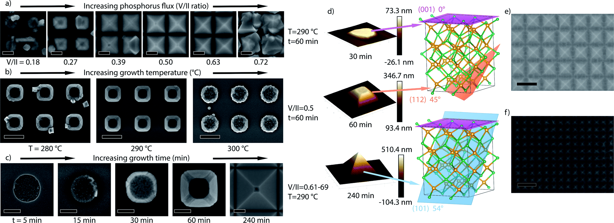 | ||
| Fig. 1 (a) SEM images of a flux series, varying the phosphorus to zinc (V/II) ratio at a constant zinc flux of 6.04 × 10⁻⁷ torr from 0.18 to 0.72 for 60 min growth time at 290 °C manipulator temperature (30 nm nominal hole size, 200 nm pitch, 100 nm scale bars). (b) SEM images of a temperature series, varying the manipulator temperature between 280 and 300 °C at a V/II ratio of 0.5 for a growth time of 60 minutes (150 nm nominal hole size, 800 nm pitch, 500 nm scale bars). (c) SEM images of a time series of a pyramid spanning from 5 minutes to 240 minutes acquired at a V/II ratio of 0.61 (0.69 for the 240 minutes sample) and manipulator temperature of 290 °C (note: last one taken at lower magnification to fit the full pyramid, 150 nm nominal hole size, 800 nm pitch, 100 nm scale bars). (d) AFM images of pyramids at different growth times and lattice structure models showing the different planes. (e) SEM image of initial stages of coalescence as seen with pyramids with a 400 nm pitch and 75 nm nominal hole size (scale bar 500 nm). (f) SEM image of a fully overgrown pyramid array with 200 nm pitch and 30 nm nominal hole size, still exhibiting a textured surface (scale bar 500 nm). | ||
Fig. 1c illustrates the shape evolution of the structures as a function of time. Growth is initiated through multiple small nuclei, which subsequently merge to fill the hole. Once the hole is filled, the material continues the faceting while also laterally overgrowing the oxide. Initially, a flat (001) top facet is observed without any clear side facets. After 30 minutes of growth, the (001) facet shrinks, with the development of (112) and (101) facets, with the latter increasingly dominating with time. This is to be expected, as through density functional theory (DFT) calculations we determined the surface energies for the facets to be E(101) = 0.60 J m−2 < E(112) = 0.84 J m−2 < E(001) = 1.03 J m−2.47 After a certain time, which depends on the hole size and pitch, a pyramid enclosed only by the most stable (101) surfaces is formed.47,48 The pyramidal shape is desirable due to it aiding in trapping light within the absorber layer.49–51Fig. 1d includes typical atomic force microscopy (AFM) images that are used to determine the facet orientation as a function of time, along with transmission electron microscopy (TEM) as presented below. As the pyramids continue to grow, they coalesce into a thin film in a LEO fashion. Larger hole sizes and smaller pitches were observed to overgrow quicker, with some representative examples of different stages of overgrowth shown in Fig. 1e and f.
To understand the epitaxial relation in greater detail, a set of focused ion beam (FIB) lamellae of pyramids from different hole sizes, zone axes, and growth times are analysed by TEM. Fig. 2a–c show the cross-sectional TEM image of pyramids observed along a [110] zone axis of indium phosphide ([100] zone axis for zinc phosphide). At the smallest nominal hole size (30 nm) for the same pitch (400 nm) we observe a more complete pyramid compared to that of the larger nominal hole sizes (60 nm and 90 nm), which in turn exhibit a higher degree of lateral overgrowth. All pyramids start with a [001] growth direction, resulting in the epitaxial relationship [001]InP/[001]Zn3P2 in the interface normal, and [110]InP/[100]Zn3P2 in the direction perpendicular to the surface (corresponding to [110]InP/[110]Zn3P2 in the pseudo-cubic configuration of zinc phosphide). Fig. 2d shows a representative selective area electron diffraction (SAED) pattern. The diffraction spots of zinc phosphide do not overlap with those of the substrate, indicating that the zinc phosphide has not taken the lattice parameter of the substrate, and has fully relaxed. The relaxation is further shown through geometric phase analysis (GPA) as presented below.
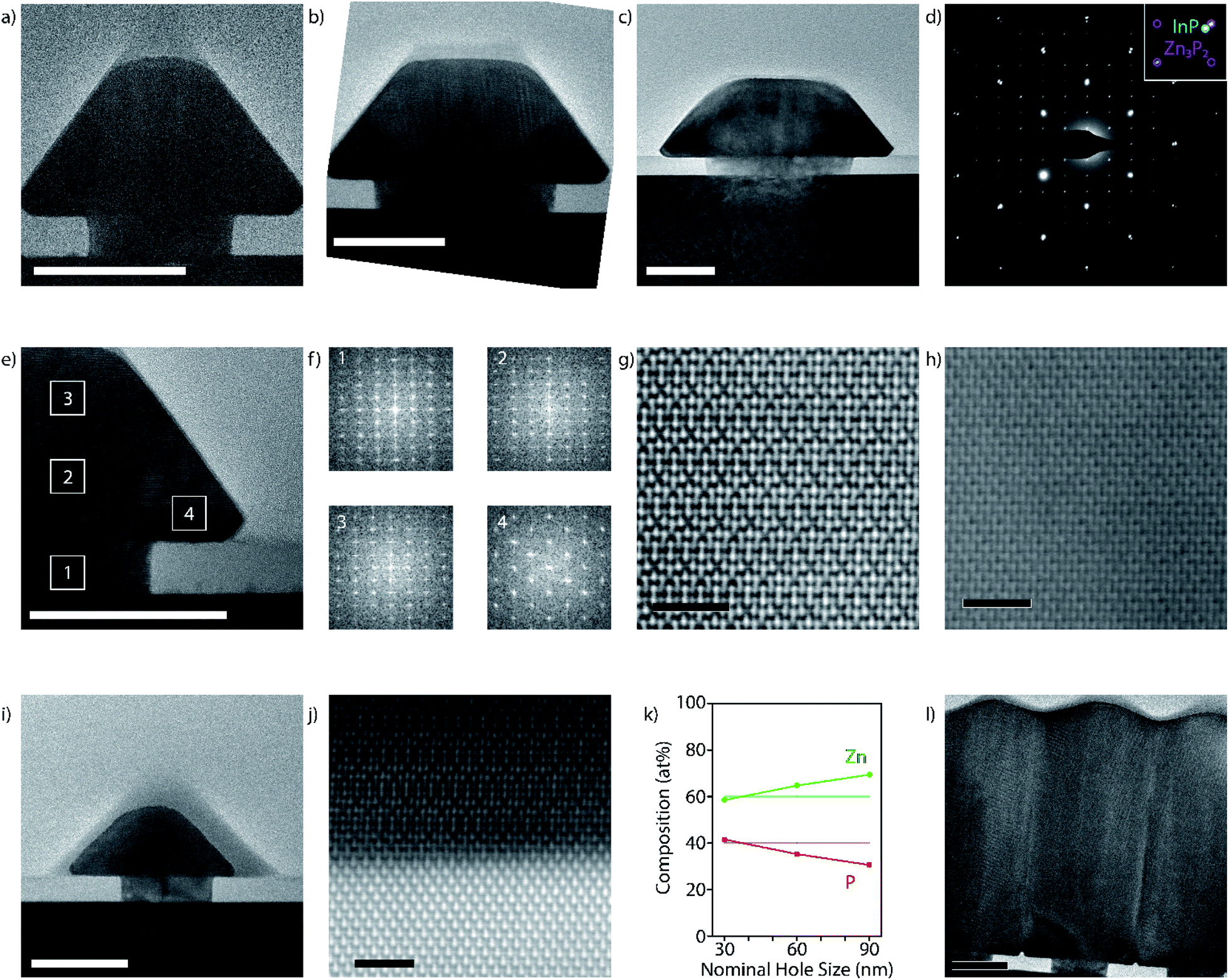 | ||
| Fig. 2 (a–c) Low-magnification HR-TEM images along the zinc phosphide [100] zone axis of pyramids grown in 30, 60, and 90 nm nominal holes for 1 hour at a V/II ratio of 0.5 and temperature of 290 °C (100 nm scale bars). (d) A representative SAED pattern showing diffraction from indium phosphide along the [110] zone axis superimposed on the relaxed zinc phosphide pattern along the [100] and [111] zone axes. (e) HR-TEM image of a part of a pyramid highlighting areas where the FFT is acquired (100 nm scale bar). (f) FFT patterns from different parts of the pyramid, where 1–3 show a [100] zone axis and 4 shows a [111] zone axis. (g and h) Aberration-corrected HAADF-STEM images of the core (g) along a [100] zone axis showing the systematic absences of zinc and the shell (h) along a [111] zone axis where the absences are not observed (2 nm scale bars). (i) Low-magnification HR-TEM image of a 30 nm nominal hole pyramid cut at 45° with respect to (a–c), resulting in a [110] zone axis with respect to zinc phosphide, highlighting the core–shell structure of the pyramids (100 nm scale bar). (j) Aberration-corrected HAADF STEM image of the zinc phosphide and indium phosphide interface, showing pseudomorphic growth (2 nm scale bar). (k) Plot of the composition dependence on the nominal hole size as measured by STEM-EDX with the horizontal lines indicating the ideal stoichiometry. (l) Low-magnification HR-TEM image of the cross-section of a coalesced film grown from 30 nm nominal holes and 200 nm pitch with identical conditions to (a–c) but with a 6 hour growth time (100 nm scale bar). | ||
Fig. 2e and f illustrate the crystalline orientation of a typical pyramid in different locations by the fast-Fourier transform (FFT) of the high-resolution (HR) TEM images. While the orientation is kept in the vertical direction, we observe that the lateral growth direction rotates 120° around the (101) facet. This also results in a change in the HR-TEM pattern. The different orientation is further confirmed by aberration-corrected high-angle annular dark-field scanning (HAADF-S)TEM imaging shown in Fig. 2g and h. The core–shell structure is also observed when looking at the pyramids through a [100] zone axis with respect to the indium phosphide, shown in Fig. 2i. A model of this change in orientation is presented further down.
Fig. 2j illustrates the nature of the interface with the substrate through aberration-corrected HAADF-STEM, where we see the Zn–P–Zn trimers aligning with the In–P dumbbells. The images show the presence of vertical atomic steps at the interface, but no misfit-dislocations are detected. This indicates a pseudomorphic epitaxial relationship between the zinc phosphide and the substrate. Energy-dispersive X-ray spectroscopy (EDX) indicates potential inter-diffusion of the indium and zinc at the interface (ESI Fig. S3†). While slight inter-diffusion between the layers is not necessarily detrimental for its properties, it could potentially be reduced by optimizing the etching for the desired hole size or by reducing the zinc pre-deposition. We also performed GPA on an aberration-corrected HAADF-STEM image of a full pyramid, shown in ESI Fig. S4.†52,53 This analysis confirms the absence of regular misfit-dislocations along the interface, while the zinc phosphide close to the interface exhibits compressive strain. Zinc phosphide slowly relaxes as it grows, resulting in a fully relaxed structure once outside of the confinement of the hole. The change in strain observed through GPA is ∼2.0%, in agreement with the literature.24–26
Next, we performed compositional mapping of the pyramids by EDX. The results as a function of the nominal hole size are illustrated in Fig. 2k. The material evolves from phosphorus-rich to zinc-rich by going from smaller to larger holes. This feature could eventually be used to locally tune the doping nature and density of the material. More detailed investigations are needed to fully characterise this phenomenon, which is outside the scope of this study.
The HR-TEM micrograph in Fig. 2l shows the coalescence of the pyramids from a 6 hour grown sample. Clear boundaries are observed indicating that the pyramids do not coalesce into a mono-crystalline film. However, the boundaries should not necessarily be detrimental to potential photovoltaic applications. Because the charge separation will occur in a vertical direction, and not in-plane, charges may not interact with the grain boundaries during operation. Furthermore, grain boundaries have been shown to not be a major obstacle for zinc phosphide applications.10,54
An atomic model of the lattice rotation around (101) is shown in Fig. 3a. This occurs by a change in the ordering of the vacant sites, inherent to the zinc phosphide crystal structure. The vacant sites are a result of the absence of zinc in 25% of the cubic sublattice of the zinc phosphide's pseudo-fluorite structure. As observed in the aberration-corrected images: we see the ordered absences of zinc atoms in the core of the pyramid, which becomes filled up towards the edge. This is consistently observed in all pyramids; however, it does not always occur at the same time for all pyramids and may even vary between facets on the same pyramid. A potential origin of this shell formation is that the new stacking sequence is energetically favoured when the growth surface shifts from (001) to (101). The fact that there is not a clear and consistent trend, and that it does not occur straight away, indicating that the driving force for this process is small; however, first-principles simulations would be needed to clarify the energetics quantitatively. This trend is even clearer when observing the pyramids along the [100] zone axis with regard to the indium phosphide (100) substrate ([110] zone axis for zinc phosphide), where we see distinct contrast between the core and the shell, which no longer seems to be on the zone axis. The atomic model for this interface, shown in Fig. 3b, indicates that the rotation previously explained will result in both parts still being on the zone axis. The disorder observed in the corners could originate from the merging of (101) facets and prevents HR-imaging. However, STEM-EDX maps (shown in ESI Fig. S3†) show that these regions are still zinc phosphide.
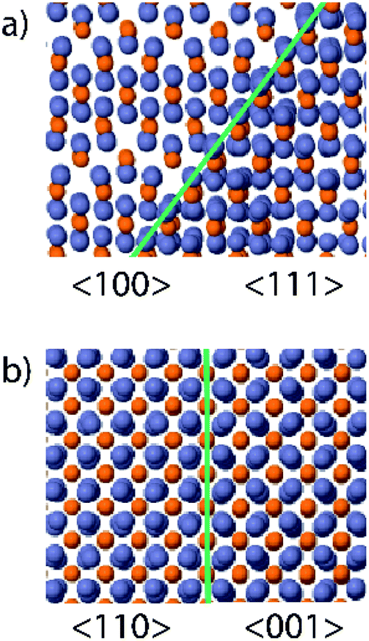 | ||
| Fig. 3 (a) Atomic model of the core–shell configuration when observed along the [100]/[111] zone axes and (b) along the [110]/[001] zone axes. Blue represents zinc and orange phosphorus. | ||
Finally, the functional properties are assessed by photoluminescence spectroscopy (PL) and conductive (C-)AFM, both performed at room temperature. The PL spectrum acquired from pyramids grown from 90 nm holes with a 600 nm pitch is shown in Fig. 4a. We observed three main emission features: (1) indium phosphide substrate emission (1.34 eV), (2) zinc phosphide bandgap emission (1.53 eV), and (3) sub-bandgap zinc phosphide emission in the region in between.6,55,56 The presence of the direct bandgap emission indicates that the material grown through SAE exhibits very high quality. This response was limited to a subset of the larger hole sizes and the lowest pitches. A more detailed study of the optical properties will be reported separately.
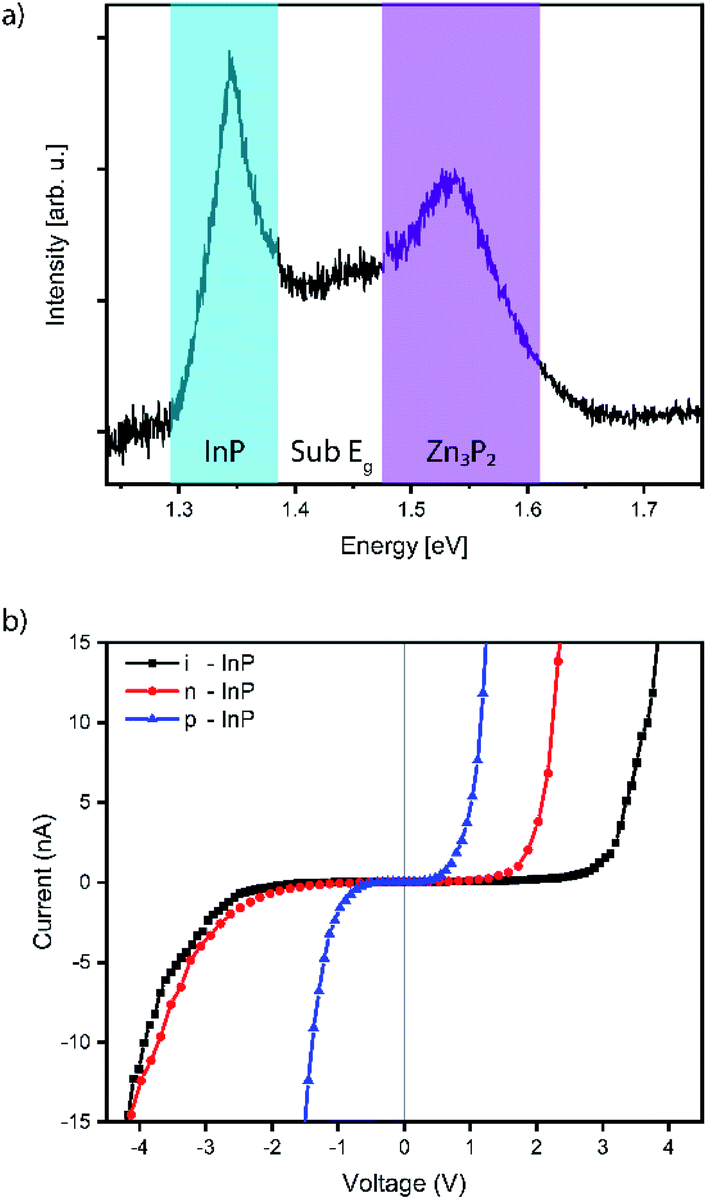 | ||
| Fig. 4 (a) PL spectrum acquired from an array with a 600 nm pitch and 150 nm nominal hole size, showing the indium phosphide, zinc phosphide, and defect emission. (b) C-AFM I–V curves of zinc phosphide grown on intrinsic, n-type, and p-type indium phosphide. | ||
C-AFM is carried out on samples grown on intrinsic, p-, and n-doped indium phosphide substrates. Representative I–V curves are shown in Fig. 4b. The measurements are carried out on pyramids with 30 nm nominal holes and a 200 nm pitch to focus only on the influence of the substrate doping as an example. All the I–V curves exhibit a current rectification behaviour under forward bias. The diode threshold voltage is highly dependent on the substrate doping (around 0.5 V, 1.5 V and 2.5 V respectively for p-, n- and intrinsic substrates). The sample grown on p-type indium phosphide shows a significant current under reverse bias. This feature may indicate a poor charge depletion at the substrate interface due to the p-type conductivity for the zinc phosphide pyramids, which is consistent with previous reports of the material.15 Considering the reverse branch of the n-type substrate I–V curve, we observe a more diode-like characteristic as would be expected for a p–n heterostructure. The I–V curve obtained on intrinsic substrates shows a wide range with a negligible current flow, which could be due to the low conductivity of the substrate. In principle, this could also be consistent with the p-type conduction of zinc phosphide.15 The influence of the hole size and pitch is also of interest due to their influence on the composition and interface area, and will be investigated in a separate study.
Conclusions
In summary, we demonstrate how to grow high-quality zinc phosphide nanostructures by SAE and its potential to obtain high-quality thin films through lateral overgrowth. We elucidate the conditions for selective growth and the mechanism by which the material nucleates inside the nanoscale holes and grows into single crystals. As the crystals develop, their surface evolves from a mixture of (001), (112) and (101) facets, into nanopyramids enclosed solely by the most stable (101) facets. The pyramids grow laterally, forming a thin film. Boundaries are observed in the coalescence. The stoichiometry of zinc phosphide depends on the hole size for a given set of conditions, from phosphorus-rich to zinc-rich with the increasing hole size. PL measurements reveal a clear transition at 1.53 eV, attributed to bandgap recombination of zinc phosphide. This further illustrates the high-quality nature of the material. C-AFM showed a diode-like behaviour when the zinc phosphide was grown on an n-type substrate, indicating the p-type nature of the material. Due to the small interface area of each pyramid with the substrate, we believe that this method is transferable to earth-abundant substrates, such as silicon, which would greatly improve the large-scale prospects of zinc phosphide-based photovoltaics, and the approach itself is a viable route for high-quality epitaxial growth of other earth-abundant materials.Conflicts of interest
There are no conflicts to declare.Acknowledgements
We acknowledge Didem Dede, Nicholas Morgan and Wonjong Kim for helpful discussions regarding SAE and the substrate patterning procedures. We thank CMi, and in particular Zdenek Benes for support with mask fabrication. Victor Boureau and Lucie Navrátilová at EPFL-CIME are acknowledged for technical support with GPA and FIB, respectively. S. E. S., E. Z. S., R. P., M. Z., J.-B. L., and A. F. i M. were supported by SNSF Consolidator grant BSCGI0-157705 and the Max-Planck-EPFL-Center for Molecular Nanoscience and Technology. N. Y. D. acknowledges the UK Engineering and Physical Sciences Research Council (EPSRC) for funding (Grant No. EP/S001395/1). V. P. was supported by Piaget. M. F. and A. F. i M. were supported by the NCCR QSIT. R. R. Z. was supported by EPFL-CIME. The DFT calculations were performed using the computational facilities of the Advanced Research Computing @ Cardiff (ARCCA) Division, Cardiff University.References
- C. Wadia, A. P. Alivisatos and D. M. Kammen, Environ. Sci. Technol., 2009, 43, 2072–2077 CrossRef CAS.
- D. Shin, B. Saparov and D. B. Mitzi, Adv. Energy Mater., 2017, 7, 1602366 CrossRef.
- L. H. Wong, A. Zakutayev, J. D. Major, X. Hao, A. Walsh, T. K. Todorov and E. Saucedo, JPhys Energy, 2019, 1, 032001 CrossRef CAS.
- W. Ki and H. W. Hillhouse, Adv. Energy Mater., 2011, 1, 732–735 CrossRef CAS.
- N. S. Lewis, Science, 2016, 351, aad1920 CrossRef.
- G. M. Kimball, A. M. Mueller, N. S. Lewis and H. A. Atwater, Appl. Phys. Lett., 2009, 95, 112103 CrossRef.
- M. Y. Swinkels, A. Campo, D. Vakulov, W. Kim, L. Gagliano, S. Escobar Steinvall, H. Detz, M. De Luca, A. Lugstein, E. Bakkers, A. Fontcuberta i Morral and I. Zardo, Phys. Rev. Appl., 2020, 14, 024045 CrossRef CAS.
- E. A. Fagen, J. Appl. Phys., 1979, 50, 6505–6515 CrossRef CAS.
- W. Shockley and H. J. Queisser, J. Appl. Phys., 1961, 32, 510–519 CrossRef CAS.
- M. Bhushan and A. Catalano, Appl. Phys. Lett., 1981, 38, 39–41 CrossRef CAS.
- M. Sun, H. Liu, J. Qu and J. Li, Adv. Energy Mater., 2016, 6, 1600087 CrossRef.
- T. Suda and K. Kakishita, J. Appl. Phys., 1992, 71, 3039–3041 CrossRef CAS.
- T. Suda, K. Kakishita, H. Sato and K. Sasaki, Appl. Phys. Lett., 1996, 69, 2426–2428 CrossRef CAS.
- J. P. Bosco, G. M. Kimball, N. S. Lewis and H. A. Atwater, J. Cryst. Growth, 2013, 363, 205–210 CrossRef CAS.
- A. Catalano and R. Hall, J. Phys. Chem. Solids, 1980, 41, 635–640 CrossRef CAS.
- J. Long, J. Electrochem. Soc., 1983, 130, 725–728 CrossRef CAS.
- R. Paul, N. Humblot, S. Escobar Steinvall, E. Z. Stutz, S. S. Joglekar, J.-B. Leran, M. Zamani, C. Cayron, R. Logé, A. G. del Aguila, Q. Xiong and A. Fontcuberta i Morral, Cryst. Growth Des., 2020, 20, 3816–3825 CrossRef CAS.
- S. Escobar Steinvall, N. Tappy, M. Ghasemi, R. R. Zamani, T. LaGrange, E. Z. Stutz, J.-B. Leran, M. Zamani, R. Paul and A. Fontcuberta i Morral, Nanoscale Horiz., 2020, 5, 274–282 RSC.
- R. Katsube, K. Kazumi, T. Tadokoro and Y. Nose, ACS Appl. Mater. Interfaces, 2018, 10, 36102–36107 CrossRef CAS.
- M. Bhushan, J. Appl. Phys., 1982, 53, 514–519 CrossRef CAS.
- G. M. Kimball, N. S. Lewis and H. A. Atwater, in Photovoltaic Specialists Conference (PVSC), 2010, pp. 1039–1043 Search PubMed.
- T. Suda, M. Kobayashi, A. Kuroyanagi and S. Kurita, Jpn. J. Appl. Phys., 1982, 21, 63 CrossRef CAS.
- S. Sudhakar and K. Baskar, J. Cryst. Growth, 2008, 310, 2707–2711 CrossRef CAS.
- M. V. Stackelberg and R. Paulus, Z. Phys. Chem., 1935, 28, 427–460 Search PubMed.
- H. S. Kim, Y. Myung, Y. J. Cho, D. M. Jang, C. S. Jung, J. Park and J.-P. Ahn, Nano Lett., 2010, 10, 1682–1691 CrossRef CAS.
- C. Pistorius, G. Clark, J. Ceotzer, G. Kruger and O. Kunze, High Temp. High Press., 1977, 9, 471–482 CAS.
- F. Glas, Phys. Rev. B: Condens. Matter Mater. Phys., 2006, 74, 121302 CrossRef.
- M. S. Gudiksen, L. J. Lauhon, J. Wang, D. C. Smith and C. M. Lieber, Nature, 2002, 415, 617–620 CrossRef CAS.
- M. T. Björk, B. J. Ohlsson, T. Sass, A. I. Persson, C. Thelander, M. H. Magnusson, K. Deppert, L. R. Wallenberg and L. Samuelson, Appl. Phys. Lett., 2002, 80, 1058–1060 CrossRef.
- M. Albani, L. Ghisalberti, R. Bergamaschini, M. Friedl, M. Salvalaglio, A. Voigt, F. Montalenti, G. Tütüncüoglu, A. Fontcuberta i Morral and L. Miglio, Phys. Rev. Mater., 2018, 2, 093404 CrossRef CAS.
- M. Friedl, K. Cerveny, P. Weigele, G. Tütüncüoglu, S. Martí-Sánchez, C. Huang, T. Patlatiuk, H. Potts, Z. Sun, M. O. Hill, L. Güniat, W. Kim, M. Zamani, V. G. Dubrovskii, J. Arbiol, L. J. Lauhon, D. M. Zumbühl and A. Fontcuberta i Morral, Nano Lett., 2018, 18, 2666–2671 CrossRef CAS.
- A. M. Raya, M. Friedl, S. Martí-Sánchez, V. G. Dubrovskii, L. Francaviglia, B. Alén, N. Morgan, G. Tütüncüoglu, Q. M. Ramasse, D. Fuster, J. M. Llorens, J. Arbiol and A. Fontcuberta i Morral, Nanoscale, 2020, 12, 815–824 RSC.
- P. Aseev, A. Fursina, F. Boekhout, F. Krizek, J. E. Sestoft, F. Borsoi, S. Heedt, G. Wang, L. Binci, S. Martí-Sánchez, T. Swoboda, R. Koops, E. Uccelli, J. Arbiol, P. Krogstrup, L. P. Kouwenhoven and P. Caroff, Nano Lett., 2019, 19, 218–227 CrossRef CAS.
- L. Desplanque, A. Bucamp, D. Troadec, G. Patriarche and X. Wallart, J. Cryst. Growth, 2019, 512, 6–10 CrossRef CAS.
- L. Güniat, P. Caroff and A. Fontcuberta i Morral, Chem. Rev., 2019, 119, 8958–8971 CrossRef.
- R. R. Li, P. D. Dapkus, M. E. Thompson, W. G. Jeong, C. Harrison, P. M. Chaikin, R. A. Register and D. H. Adamson, Appl. Phys. Lett., 2000, 76, 1689–1691 CrossRef CAS.
- C.-Y. Chi, C.-C. Chang, S. Hu, T.-W. Yeh, S. B. Cronin and P. D. Dapkus, Nano Lett., 2013, 13, 2506–2515 CrossRef CAS.
- A. R. Bushroa, C. Jacob, H. Saijo and S. Nishino, J. Cryst. Growth, 2004, 271, 200–206 CrossRef CAS.
- T. Nishinaga, T. Nakano and S. Zhang, Jpn. J. Appl. Phys., 1988, 27, L964–L967 CrossRef CAS.
- K. Hiramatsu, K. Nishiyama, M. Onishi, H. Mizutani, M. Narukawa, A. Motogaito, H. Miyake, Y. Iyechika and T. Maeda, J. Cryst. Growth, 2000, 221, 316–326 CrossRef CAS.
- Y. Ohshita and A. Ishitani, J. Appl. Phys., 1989, 66, 4535–4537 CrossRef CAS.
- N. P. Kobayashi, J. T. Kobayashi, X. Zhang, P. D. Dapkus and D. H. Rich, Appl. Phys. Lett., 1999, 74, 2836–2838 CrossRef CAS.
- D. Ren, W. Zhou and P. D. Dapkus, Appl. Phys. Lett., 2005, 86, 111901 CrossRef.
- M. Ghasemi, E. Stutz, S. Escobar Steinvall, M. Zamani and A. Fontcuberta i Morral, Acta Mater., 2019, 6, 100301 CrossRef.
- J. D. McKinley and J. E. Vance, J. Chem. Phys., 1954, 22, 1120–1124 CrossRef CAS.
- H. Melville and S. Gray, J. Chem. Soc., Faraday Trans., 1936, 32, 1026–1030 RSC.
- N. Y. Dzade, Phys. Chem. Chem. Phys., 2020, 22, 1444–1456 RSC.
- M. Albani, R. Bergamaschini, M. Salvalaglio, A. Voigt, L. Miglio and F. Montalenti, Phys. Status Solidi B, 2019, 256, 1800518 CrossRef.
- D. Liang, Y. Huo, Y. Kang, K. X. Wang, A. Gu, M. Tan, Z. Yu, S. Li, J. Jia, X. Bao, S. Wang, Y. Yao, H.-S. P. Wong, S. Fan, Y. Cui and J. S. Harris, Adv. Energy Mater., 2012, 2, 1254–1260 CrossRef CAS.
- E. C. Garnett, B. Ehrler, A. Polman and E. Alarcon-Llado, ACS Photonics DOI:10.1021/acsphotonics.0c01045.
- C. Battaglia, C.-M. Hsu, K. Söderström, J. Escarré, F.-J. Haug, M. Charrière, M. Boccard, M. Despeisse, D. T. L. Alexander, M. Cantoni, Y. Cui and C. Ballif, ACS Nano, 2012, 6, 2790–2797 CrossRef CAS.
- Y. Zhu, C. Ophus, J. Ciston and H. Wang, Acta Mater., 2013, 61, 5646–5663 CrossRef CAS.
- M. J. Hÿtch, E. Snoeck and R. Kilaas, Ultramicroscopy, 1998, 74, 131–146 CrossRef.
- M. Bhushan, Appl. Phys. Lett., 1982, 40, 51–53 CrossRef CAS.
- F. Briones, F. Wang and R. Bube, Appl. Phys. Lett., 1981, 39, 805–807 CrossRef CAS.
- N. Mirowska and J. Misiewicz, Semicond. Sci. Technol., 1992, 7, 1332–1336 CrossRef CAS.
Footnote |
| † Electronic supplementary information (ESI) available. See DOI: 10.1039/d0na00841a |
| This journal is © The Royal Society of Chemistry 2021 |