
 Open Access Article
 This Open Access Article is licensed under a Creative Commons Attribution-Non Commercial 3.0 Unported Licence
Large plasmonic color metasurfaces fabricated by super resolution deep UV lithography†
Matthias
Keil
a,
Alexandre Emmanuel
Wetzel
a,
Kaiyu
Wu
bc,
Elena
Khomtchenko
a,
Jitka
Urbankova
a,
Anja
Boisen
b,
Tomas
Rindzevicius
b,
Ada-Ioana
Bunea
 a and
Rafael J.
Taboryski
*a
a and
Rafael J.
Taboryski
*a
aDTU Nanolab, National Centre for Nano Fabrication and Characterization, Technical University of Denmark, Ørsted Plads, Building 347, DK-2800 Kgs. Lyngby, Denmark. E-mail: rata@dtu.dk; Tel: +45 45258101
bDTU Health Tech, Department of Health Technology, Technical University of Denmark, DK-2800 Kgs. Lyngby, Denmark
cNational Key Laboratory of Science and Technology on Micro/Nano Fabrication, Department of Micro/Nano Electronics, School of Electronic Information and Electrical Engineering, Shanghai Jiao Tong University, Shanghai, 200240, P. R. China
First published on 18th February 2021
Abstract
In this paper, we demonstrate plasmonic color metasurfaces as large as ∼60 cm2 fabricated by deep UV projection lithography employing an innovative combination of resolution enhancement techniques. Briefly, in addition to the established off-axis dipole illumination, double- and cross-exposure resolution enhancement of lithography, we introduce a novel element, the inclusion of transparent assist features to the mask layout. With this approach, we demonstrate the fabrication of relief arrays having critical dimensions such as 159 nm nanopillars or 210 nm nanoholes with 300 nm pitches, which is near the theoretical resolution limit expressed by the Rayleigh criterion for the 248 nm lithography tool used in this work. The type of surface structure, i.e. nanopillar or nanohole, and their diameters can be tailored simply by changing the width of the assist features included in the mask layout. By coating the obtained nanopatterns with thin layers of either Au or Al, we observe color spectra originating from the phenomenon known as localized surface plasmon resonance (LSPR). We demonstrate the generation of color palettes representing a broad spectral range of colors, and we employ finite element modelling to corroborate the measured LSPR fingerprint spectra. Most importantly, the ∼60 cm2 nanostructure arrays can be written in only a few minutes, which is a tremendous improvement compared to the more established techniques employed for fabricating similar structures.
Introduction
When light interacts with dielectric materials containing embedded metallic nanoparticles, the particles behave like nano-resonators, resulting in the excitation of coherent and collective conduction-electron-density oscillations in the metal. These oscillations are called surface plasmons1–3 and can greatly enhance various light–matter interactions due to their ability to confine the electrical field at dimensions much smaller than the wavelength of the incident light. Surface plasmon effects are widely used in biosensing, as recently reviewed elsewhere.4 Other applications include photocatalysis,5 heat generation,6 photoacoustic imaging,7 and the generation of structural colors,8 which is of particular interest for this paper.Surface plasmons have been exploited since ancient times to produce the vivid colors observed in stained glass fabricated using metallic powders. However, many centuries passed before the underlying phenomena involved in creating the beautiful colors was identified as localized surface plasmon resonance (LSPR) in metallic nanoparticles.9 The color effects can be explained by the dissipative nature of the electron density oscillations, where the oscillation modes are excited by specific wavelengths of light, and give rise to extinction of the corresponding colors in the reflectance and transmittance spectra.2 The field of plasmonic structural colors is rapidly growing, and a more detailed description of color mapping and other recent advances was reviewed by Song et al.8 Typically, plasmonic color effects associated with metal nanoparticles are volume effects, where the colors are defined by the size and shape of the metallic nanoparticles, and the dielectric properties of the surrounding media.1 When it comes to surfaces, plasmonic colors are predominantly demonstrated with regular arrays of nanofabricated metallic structures,10–17 and there is significant interest in literature for the large scale fabrication of plasmonic color filters.18–21
Plasmonic color effects are only observed for metallic nanosized structures smaller than the excitation wavelength for LSPR, which is why such features are referred to as “sub-wavelength” structures.22,23 Hence, plasmonic color generation on solid surfaces requires the critical dimensions (CD) of the metallic nanostructures to be smaller than roughly half the excitation wavelength, i.e. effectively below ∼200 nm.17,24,25 This requirement severely limits the applicability of most lithographic techniques for fabrication of plasmonic metasurfaces. Instead, most studies are carried out using electron beam lithography to define the structures.11,12,26–31 Although electron beam lithography is indeed suitable in terms of the required resolution, as it can easily produce structures with CD below 200 nm, the throughput of the technique is extremely low. Therefore, a different approach is required for producing large area plasmonic color surfaces. Although replication roadmaps by use of nanoimprint lithography11,12 and roll-to-roll processes exist,14,32,33 large area master origination methods for the fabrication of plasmonic metasurfaces have not yet been demonstrated. When looking into the nanofabrication toolbox,34 a number of bottom-up methodologies35 such as block-copolymer nanolithography,36–41 and colloidal lithography42,43 may offer promising roadmaps for origination of large area plasmonic surfaces. In addition, depending on the light source used, interferometric lithography may also be a suitable candidate for the fabrication of large area nanoscale patterns, but this technique usually requires complicated custom made setups.44
A more direct route is to employ projection photolithography tools similar to the ones used by the semiconductor industry for the fabrication of computer chips.45–47 These tools range from standard I-line photolithography using 365 nm mercury arc lamps with resolution down to 350 nm to extreme UV (EUV) using a 13.5 nm Sn laser-produced plasma light sources featuring sub 20 nm resolution.48 EUV tools are however not available for academic research for the time being, and I-line lithography is not capable of producing structures with CD below 200 nm. To improve resolution, i.e. to decrease the feature sizes and pitches of printed patterns with acceptable tolerances, numerous resolution enhancement techniques (RET) have been introduced over the last decades in projection lithography. The range of applied RET comprise optical proximity corrections, such as the use of sheriff and assist features, lithography-based/etch-based double patterning, cross exposure, source mask optimization, and the application of alternating phase-shift masks and off-axis illumination.47,49–51 In the case of periodic patterns with pitches at the resolution limit, off-axis illumination (OAI) is the preferred RET for maximizing resolution. Hence, with OAI using e.g. a dipole source, pattern definition can be obtained with a line-grating mask theoretically having a pitch down to half the one obtained with center-axis illumination for the same tool.
In this paper, we demonstrate the fabrication of large area plasmonic surfaces by employing a innovative RET combination on a direct projection lithography deep UV (DUV) stepper tool from the ‘90s. Briefly, we supplement some of the already mentioned RETs of dipole OAI and cross exposure, with a novel approach of altering the linewidths by adding transparent assist feature (AF) lines to the mask layout. This process enables fabrication of hole and pillar patterns with different CD without changing the exposure dose and focus, and the smallest feature size generated is ∼100 nm. The combined RET is a pure exposure process, thus no post exposure processes (e.g. post exposure bake or etching) are applied between the different exposure steps, which renders complicated alignment procedures unnecessary. Table 1 shows a brief comparison between this approach and other nanopatterning methods that show promise as large area master origination methods because of their ability to produce nanostructured patterns larger than 1 cm2.
| This work | Telecka et al.41 | Cataldo et al.42 | Xia et al.44 | |
|---|---|---|---|---|
| Nanopattern fabrication technique | Projection photolithography + RET combination | Block copolymer lithography (with reactive ion etching) | Colloidal lithography (with O2 plasma etching) | Interferometric lithography |
| Resolution | 90 nm wall thickness, 159 nm pillars, 210 nm holes | Pitch ∼ 72 nm | ∼100 nm (authors claim 50 nm) | 48–91 nm (¼ of laser wavelength), 33 nm with water immersion |
| Patterns | Pillars or holes | Holes or dots (pillars) | Split ring resonators | Various periodic patterns |
| Pattern size | 80 × 72 mm2 (∼60 cm2) written in a few minutes, 22 × 22 mm2 for single exposure | 100 mm wafer | 1 cm2, limited by the homogeneous PMMA area fabricated using spin-coating | 1 cm2 or more |
Using the innovative RET combination for the deep UV lithography process, we demonstrate super-resolution fabrication of a color palette of structural colors, including blue, green, and red shades, merely by changing the linewidth of the AF lines on the mask. This approach allows us to exploit the DUV stepper technology for the fabrication of large area plasmonic metasurfaces, i.e. covering most of a 150 mm wafer.
Materials and methods
Plasmonic metasurface fabrication
Projection lithography was carried out with a Canon FPA-3000EX4 stepper tool having a projection lens' NA of 0.6 with reduction factor of 5. The tool is fitted with a 248 nm KrF Excimer laser Cymer/ELS-5300 (output 10 W, pulse frequency 1 kHz, intensity 3300 W m−2). The specified general resolution is 250 nm, independent from the type of pattern. The maximum print area of one single exposure is 22 × 22 mm2. Grating patterns with larger sizes are produced by stitching together single exposure areas.The material stack consisted of a 360 nm thick layer of a positive tone resist (KRF-M230Y from JSR) on a 65 nm thick bottom anti-reflective coating (BARC, DUV-42s from Brewer Science), both spin coated onto 150 mm double side polished silicon wafers. A source stopper plate fitted with two off-axis symmetrical apertures was employed as dipole illumination source with σC = 0.6 and σR = 0.2. The exposure sequence consisted of 4 sequential exposure steps. After the first exposure step, the wafer was translated along the x-axis by a half-pitch. After the second step, both the illumination source and the mask containing the assist features were rotated by 90°. After the third step, the wafer was translated along the y-axis by a half-pitch. After the exposure sequence, a post exposure bake (60 s; 130 °C) step was included, and finally the structures were developed (60 s in AZ 726 MIF Developer from MicroChemicals). The final height of the resulting nanoholes and nanopillar structures was ∼330 nm.
10 nm thick films of either Al or Au were deposited onto the samples by directional electron-beam evaporation using the evaporator tools Temescal FC-2000 (Ferrotec) or QCL 800 (Wordentec). In all cases, the base pressure directly before metal deposition was lower than 10−6 Torr and the deposition rate was 2 Å s−1.
Resolution enhancement simulations
Aerial image simulations of the projection lithography process were carried out with the Prolith™ software provided by KLA-Tencor. The theoretical investigations were focused on the formation of the aerial image and of the optical image inside the resist layer. The values for the real and imaginary part of the refractive indices of the employed materials (resist, BARC and silicon wafer) were provided by JSR Corporation and KLA-Tencor.Scanning electron microscopy
Samples were characterized by scanning electron microscopy (SEM) using a Zeiss Supra 40VP. For the investigation of metallized and non-metallized resist samples, the electron accelerating voltage (EHT) was 1.5 kV and an Everhart–Thornley secondary electron detector was used to collect the scattered electrons from the surface.Optical reflectance measurements
The samples' reflectance spectra were measured using the optical setup shown in Fig. S1.† A broadband halogen light source (Euromex LE.5210) was used to illuminate the sample along with lenses L1 (f = 100 mm) and L2 (f = 50 mm). A 50![[thin space (1/6-em)]](https://www.rsc.org/images/entities/char_2009.gif) :50 beamsplitter (Thorlabs CM1-BS013) was placed in the beam path to retrieve the reflected light from the sample, and lens L3 (f = 36.01 mm) transferred the reflected light to a multimode fiber connected to a spectrometer (Ocean Optics USB2000+VIS-NIR-ES). Our measurements were made at normal incidence and used a collection angle of 28.5°. We first measured the spectrum of a reference sample, i.e. a silicon wafer with a 120 nm Al layer, before acquiring spectra for our samples. The silicon wafer coated with a 120 nm thick Al layer approximates a perfect mirror in the visible light range. The reflectance of each sample was then calculated as the ratio between the sample spectrum and reference spectrum. Furthermore, we retrieved the RGB as well as the XY CIE color coordinates from the measured reflectance spectra using the CIE RGB color matching functions.52
:50 beamsplitter (Thorlabs CM1-BS013) was placed in the beam path to retrieve the reflected light from the sample, and lens L3 (f = 36.01 mm) transferred the reflected light to a multimode fiber connected to a spectrometer (Ocean Optics USB2000+VIS-NIR-ES). Our measurements were made at normal incidence and used a collection angle of 28.5°. We first measured the spectrum of a reference sample, i.e. a silicon wafer with a 120 nm Al layer, before acquiring spectra for our samples. The silicon wafer coated with a 120 nm thick Al layer approximates a perfect mirror in the visible light range. The reflectance of each sample was then calculated as the ratio between the sample spectrum and reference spectrum. Furthermore, we retrieved the RGB as well as the XY CIE color coordinates from the measured reflectance spectra using the CIE RGB color matching functions.52
Electromagnetic field simulations
Three-dimensional finite element method (FEM) simulations were performed using COMSOL MULTIPHYSICS version 5.5. A domain-backed port, located at the top of the solution domain, was used to excite the linearly polarized incident electromagnetic field. A perfectly matched layer (PML) was employed to eliminate nonphysical reflections. Scattering boundary conditions were employed on the top and bottom boundaries of the PML layer to further reduce reflection. For the side planes of the solution domain, Floquet periodicities were used. The geometry of the simulated structures was modeled according to the SEM images. Materials were modeled by their complex refractive indexes as functions of the wavelength. Complex refractive indexes of Au and Al used in the models were measured on a 120 nm thick Au film and a 120 nm thick Al film, respectively. The structures were surrounded by vacuum. The electromagnetic field distribution was calculated by solving the full field. The reflectance was calculated by R = (I0 − 〈Sn〉)/I0, where I0 is the intensity of the incident light and Sn is the Poynting vector in the incident medium perpendicular to the structural surface. Linear treatments were applied to the simulated spectra to improve clarity.Results & discussion
For the DUV stepper tool, the resolution limit for periodic patterns is usually expressed in terms of the Rayleigh criterion that define the best obtainable resolution for an optical system as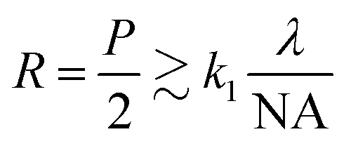 | (1) |
Without RET, the 248 nm DUV stepper tool typically yields CD ≳ 250 nm for NA = 0.6 corresponding to k1 ∼ 0.6. Super resolution is obtained by reduction of the k1-factor in the Rayleigh criterion (eqn (1)) towards its theoretical limit of 0.25, and OAI is the best RET option.53,54 With OAI using e.g. a dipole source, pattern definition can be obtained with a line-grating mask theoretically having a pitch down to half the one obtained with center-axis illumination for the same tool. However, lens aberration effects, wafer roughness, and finite resist thickness make it practically impossible to reach the theoretical resolution limit. Here, we report a novel RET approach based on OAI double exposure and cross exposure, supplemented by the inclusion of transparent assist feature (AF) lines of various widths to the mask layout. With this approach, we obtain k1 ∼ 0.38, which is comparable to state-of-the-art in the semiconductor industry using this kind of DUV stepper tool.53
In Fig. 1, we show an overview of the process and two examples of printed plasmonic metasurfaces. Fig. 1a shows a schematic of the beam traced through the optics of the DUV tool used in this study. If the on-axis illumination source is replaced by a dipole source (two symmetrically placed sources in off-axis position), the −1st diffraction order of the beam illuminating the mask from its right side and the +1st order illuminating from the left will fall outside of the lens pupil. However, the 0th, +1st and −1st orders will pass through the lens symmetrically and form an image. In terms of Fourier optics, this corresponds to keeping +1st and −1st order spatial frequency Fourier terms to represent the periodic pattern whereas the 0th order yields a non-diffractive bias. The exposure sequence is shown in Fig. 1b. The first and second exposures are done with the same dipole illumination but with a half pitch wafer translation along the x-axis. Then both the illumination source and the mask are rotated by 90° before the third exposure. For the fourth and last exposure, the wafer is again moved by half a pitch length, but now along the y-direction. The pitch and space width of the line-grating are kept at 600 nm and 150 nm respectively, but transparent AF lines ranging from 100 to 150 nm (in steps of 10 nm) are added to the mask layout (see also ESI, Fig. S2†). In Fig. 1c, we show the resulting resist patterns after post-exposure bake and development. We see that in this example, we obtain holes with diameters of ∼210 nm and pillars with diameters of ∼159 nm for the two extreme values of AF widths, 100 nm and 150 nm respectively, arranged in a 2-dimensional 300 nm pitch array. After directional coating of the developed resist patterns with 10 nm thick Al or Au, plasmonic metasurfaces are formed, and plasmonic color generation is readily observed. This is shown in the colored inserts of the scanning electron micrographs. The shown colors are obtained from computed RGB color coordinates, which in turn are extracted from measured reflectance spectra. See also ESI, Fig. S3† for the full AF range.
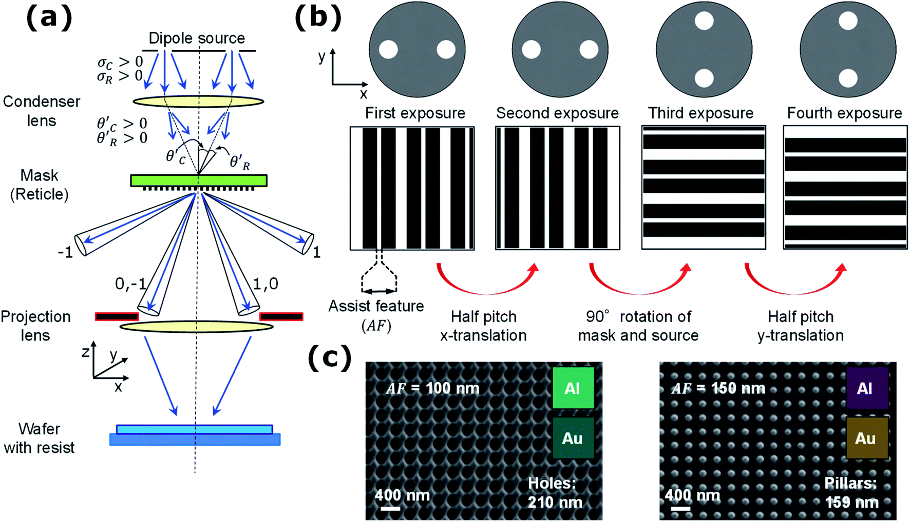 | ||
| Fig. 1 (a) Schematic of the beam trace through the DUV stepper tool. σC is the off-center coherence factor – which describes the position of the two apertures on the source – corresponding to the angle of incidence on the mask (reticle) of θ′C whereas σR is the finite radius of the circular source apertures corresponding to a cone angle of incidence on the mask (reticle) of θ′R. The dipole illumination results in symmetrical 0th, +1st and −1st diffraction order cones of light from the mask grating passing the projection lens pupil, before it is projected onto the wafer through the reduction factor of the projection lens. In this work, the reduction factor is 5. (b) A source stopper plate fitted with two off-axis symmetrical apertures constitutes the dipole illumination source with σC = 0.6 and σR = 0.2. The second exposure is done after translation of the wafer through a half pitch distance along the x-axis before the cross exposure is carried out after rotation of both the mask and the stopper plate. The fourth and final exposure is done after yet another wafer translation by a half pitch, this time along the y-direction. While the pitch on the mask and the transparent spacer lines are kept constant at 600 nm, and 150 nm respectively, the transparent assist feature (AF) lines are varied in steps of 10 nm between 100 nm and 150 nm. Due to the 5× lens reduction all dimensions of the patterns on the mask are 5× larger (c) Two examples of scanning electron microscope (SEM) images of developed resist patterns that have undergone the dipole illumination and double/cross exposure with varied AF widths. This particular exposure results in holes with diameters of ∼210 nm and pillars with diameters of ∼159 nm, for the two extreme values of AF widths, i.e. AF = 100 nm and AF = 150 nm, respectively. The insets show plasmonic color generation from the printed surfaces after directional coating of the developed structure patterns with 10 nm thick Al or Au respectively. The color patches are obtained from computed RGB color coordinates extracted from measured reflectance spectra. | ||
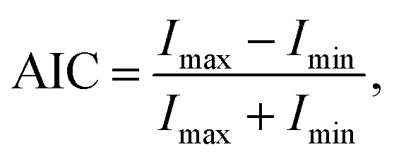
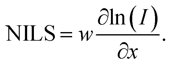
In order to determine the exposure conditions required to obtain a given resist relief, we simulated cross-exposure processes with different illumination source shapes to obtain aerial images corresponding to hole and pillar patterns with quadratic symmetry and pitches of 300 nm (see ESI, Fig. S4†). An aerial image represents the optical image of the mask pattern, projected onto the image plane of the projection lens.48 Because the image is formed in air and not in a resist, the performance of the illumination tool can be simulated independently from both resist properties and subsequent post processes, i.e. post-exposure bake and development. The aerial image contrast (AIC, eqn (2)) and the normalized image log-slope (NILS, eqn (3)) were used as metrics to quantify the optical performance for the different single and cross-exposure processes:
 | (2) |
 | (3) |
AIC describes the degree of modulation in the aerial image having a maximum of 1. Here Imax and Imin are the maximum and minimum normalized light intensities. NILS is the slope of the normalized natural logarithm of the aerial image intensity function I at the edges of the target CD, whereas w is the target width. NILS is a metric for the edge definition. AIC and NILS were determined both in focus and in defocus positions to estimate the focus range inside the finite resist thickness. The simulations revealed that dipole illumination with double line cross exposure (DLCE) and application of the AF generally yields the highest values of NILS and AIC, when compared to other exposure modes of the stepper (see ESI, Fig. S5†). Here, “double line” refers to using a double linewidth of the opaque bands on the mask pattern (see Fig. 1b). This results in a mask pitch that is twice as large as the target pattern pitch, as e.g. the 600 nm pitch referred to in Fig. 1b yields a structure pitch of 300 nm when employing DLCE (see also ESI, Fig. S2†). The assist features in the DLCE process are transparent bands. Thus, a larger AF width adds more light in the image plane and increases the intensity of the areal image. This in turn decreases the pillar width in the real exposure. On the other hand, when the widths of the AF are increased, a lower dose is required to print a particular pattern with the same dimensions. However, simulations of NILS and AIC show that the width of the AF does not affect the quality of the areal image. This is shown in ESI, Fig. S5,† a category plot, which compares simulations of NILS and AIC for exposures with different assist feature sizes and source shapes. We see that, while dipole illumination is not beneficial for large pitches, the introduction of AF improves dipole illumination with respect to the other illumination modes. It is remarkable that the width of the AF does not affect the areal image parameters significantly. On the other hand, compared to the results of the cross-exposure process (Fig. S4 and S5†) single exposure processes with similar source shapes are characterized by much lower NILS and AIC values (not shown here).
In Fig. 2, we document the plasmonic color generation from the fabricated surfaces coated with thin metal layers (10 nm of Au or Al). The colors of the metallized resist patterns are shown in the form of color palettes (Fig. 2b). By varying the widths of AF on the mask, we see a transition from hole-arrays to pillar-arrays in the resist after development (see also ESI, Fig. S3†). Apart from the widths of AF, this transition depends on the focus offsets employed during exposure. The color palettes obtained with different focus offsets are included to demonstrate the color stability upon focus variations that could occur during the exposure process due to e.g. wafer roughness, lens aberrations and inhomogeneous focus offsets at different exposure positions on the wafer. The 0 μm defocus is related to the “best focus”, i.e. a focal point in the resist at a position approximately a third of the resist thickness below the surface of the resist. For a dose of 65 J m−2, employed for the structures shown in Fig. 1c and 2, this transition happens at AF = 120 nm, so that assist features below 120 nm yield hole array surfaces, whereas assist features widths of 120 nm and above yield pillar array surfaces. Whilst a defocus smaller than 0.2 μm has very little influence on the observed plasmonic color generation, a defocus of 0.2–0.4 μm has a more noticeable effect.
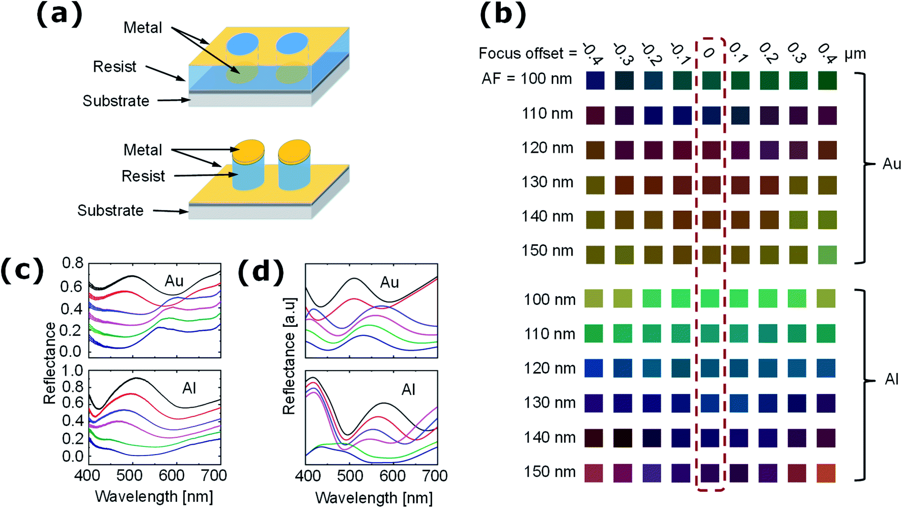 | ||
| Fig. 2 (a) Schematic of the metalized resist structures. For AF = 100 nm, the exposure yields an array of holes in the resist after development, while for AF = 150 nm, the exposure yields a pillar array after development. The substrate consists of a Si wafer coated with a bottom anti-reflective coating (BARC). (b) Color palette obtained after metallization with 10 nm of Au (top) or Al (bottom) after exposure using assist feature sizes from AF = 100 nm to AF = 150 nm varied in 10 nm steps, and focus offsets varied from −0.4 μm to +0.4 μm in relation to the focus plane of the exposure projection lens in 0.1 μm steps. The best focus exposures corresponding to a focus-offset of 0 μm are marked. Color patches represent computed RGB color coordinates extracted from measured reflectance spectra. (c) Reflectance spectra obtained after best focus exposure, development and coating with 10 nm Au (top) and 10 nm Al (bottom). Plots corresponding to the variation of assist features, from AF = 100 nm (lowest plot) to AF = 150 nm (highest plot) in steps of 10 nm. Each plot is offset by 0.1 along the y-axis from the previous plot for clarity (baseline is the AF = 100 nm plot). (d) Finite element simulated reflectance spectra corresponding to the measured data shown in panel (c). | ||
In order to ensure that colors do not depend on the light source used, we obtain the colors in Fig. 2b in the form of RGB color coordinates from the measured reflectance spectra that are normalized with the spectrum from the light source. The ESI† shows the CIE diagrams with the measured colors in Fig. S6,† and the RGB color coordinates corresponding to the palettes displayed in Fig. 2c in Table S1.† We see that whereas we do not obtain pure primary red, green and blue colors, we obtain mixed colors where one primary value typically dominate. For metallization of the resist structures with 10 nm Al, we see a dominant peak in the reflectance spectrum developing from the green part of the spectrum around 500 nm, when AF widths are increased from 100 nm to 150 nm. Hence, for the bright green color, obtained with Al coating of the developed resist (at 0 μm defocus) with AF = 100 nm, we get (RGB) = (0, 0.616, 0.467), whereas the corresponding most blue color for AF = 130 nm yields (RGB) = (0, 0.314, 0.470), and for the most red color for AF = 150 nm we have (RGB) = (0.387, 0.101, 0.230). Whereas the Al metallization exhibits the most pure green colors, metallization with Au yield the most pronounced red colors with e.g. AF = 140 nm yielding (RGB) = (0.542, 0.368, 0.228) for in focus exposure. The Au coated samples however also tend to have high contents of green, resulting in brownish shades.
It can be seen from Fig. 2d that (i) for the Au structures, the simulated reflectance spectra agree well with those obtained experimentally. (ii) For the Al structures, the simulated reflectance spectra have similar spectral fingerprints compared to the measured ones, but there is a red shift of ∼60 nm. This red shift may be caused by a difference between the complex refractive index values as a function of wavelength for Al used in the simulation and that of the real structures, which could be attributed to the thickness of Al used in this study. The influence of the metal layer thickness on the refractive index has previously been measured for Au and Ag.55 A similar behavior is expected for thin Al layers, but, to the best of our knowledge, the complex refractive index of 10 nm thick Al layers cannot be found in literature. In addition to the thickness-related refractive index issue, minor differences between the simulated and the measured reflectance spectra may appear due to the following factors: (i) in the simulation, the geometry of the structures is identical in every period. However, structural variations across periods may exist in the real structures. (ii) In the simulation, the nanopillars and the nanoholes are perfect cylinders, which is slightly different from the real structures. (iii) In the simulation, all reflected and scattered light contribute to the reflectance, while only a portion of the scattered light contributes to the measured reflectance spectra due to the collection angle limitation in the optical reflectance measurement setup.
We also investigated the influence of different linear polarizations at normal incidence on the plasmonic color generation for Al coated structures. The results are shown in Fig. 3. The color response was measured experimentally for linear polarizations oriented at angles of 0°, 45° and 90° relative to the structure arrays, and the corresponding CIE diagrams are shown. We determined that the influence of the linear polarization rotation is very limited, especially for the features printed with a focus offset of 0 μm. Furthermore, the finite element model simulations shown in Fig. S7† confirm that the filter properties of the Au metasurfaces at normal incidence also are nearly independent of the linear polarization direction. This is attributed to: (i) the symmetry of the structure, resulting in the same LSPR mode being excited for a single unit structure under different linear polarization directions. (ii) The relatively large pitch of 300 nm, with which the LSPR couplings among the periods become negligible. This is also reflected in the field distribution in Fig. S7† by the very weak field enhancement near adjacent periods.
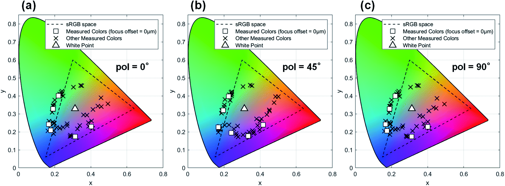 | ||
| Fig. 3 CIE diagrams for the Al metasurfaces obtained with linear polarizations of (a) 0°, (b) 45°, and (c) 90° measured relatively to the surface structure array. | ||
The similar spectral fingerprints of the simulated and the measured reflectance spectra validate our understanding of the localized surface plasmon resonance (LSPR) modes of the fabricated structures. To demonstrate, Fig. 4 shows the calculated cross-sectional distributions of the electric field enhancement, for one period of Au nanopillar (AF = 150 nm) and Au nanohole (AF = 100 nm) arrays at excitation wavelengths corresponding to the reflectance maxima and minima in the simulated spectra shown in Fig. 2d. It can be seen from Fig. 4 that the main LSPR mode for the Au nanopillar and the Au nanohole array, is the Au nanodisc and the Au nanohole mode, respectively.12 The experimental measurements and simulations described herein are for normal incidence. It is likely that non-normal incidence angles would introduce additional LSPRs oscillating perpendicular to the structural surface and could result in differences in the observed plasmonic color generation. However, this was not investigated as part of the current study.
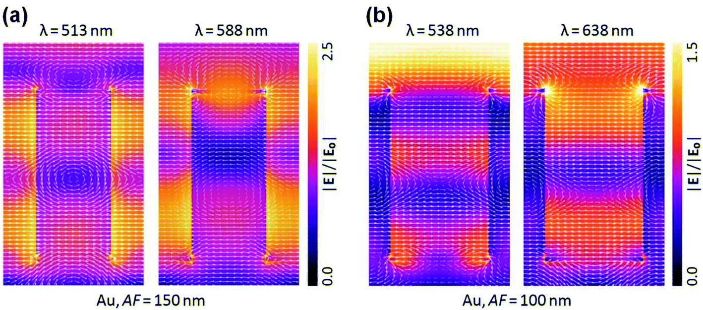 | ||
| Fig. 4 Simulated cross-sectional distributions of the electric field enhancement for one period of the (a) Au nanopillar array (AF = 150 nm) and (b) Au nanohole array (AF = 100 nm) for excitation wavelengths corresponding to the reflectance maxima and minima from the simulated spectra shown in Fig. 2d. | ||
Combining the field distributions shown in Fig. 4 with the simulated reflectance spectra from Fig. 2d, it can be concluded that the LSPR wavelengths result in the reflectance minima, and that the LSPR wavelengths can be tuned by altering the structural feature size. In addition, Fig. 4 reveals that the strengths of the LSPR relate to the interference between the incident and the reflected light. Resonances are achieved when the Au nanodiscs (AF = 150 nm) and the Au nanoholes (AF = 100 nm) are near the constructive interference patterns of the excitation fields. This means that by changing the aspect ratio of the structures, further tuning of the reflectance, i.e., color, could be achieved.
Kumar et al. reported a pixel size as small as 250 nm, i.e. close to the diffraction limit of optical microscopy.11 However, such small pixel sizes are not needed for color generation. Fig. S3† contains SEM images showing resist patterns for different hole and pillar arrays with different critical dimensions, which are used in the fabrication of plasmonic color arrays. The pitch of the structures – in horizontal and vertical direction – is 300 nm (see Fig. S2†). With an optical microscope having its resolution in the micrometer range, an array containing at least 10 structures in each direction (or approx. 3 × 3 μm2) is needed to observe a distinct color reflection. Hence, the proposed technology will allow in excess of 71 million pixels per square inch and 6 colors. There is also an issue regarding alignment accuracy: In one pixel field the maximum alignment offset between the first two exposures and the two exposures with the 90° rotated reticle is ∼60 nm. Inside the individual color pixel this misalignment does not affect the efficiency of the array, however on the edges between different pixels there will be a region of maximum 60 nm with color blur. This is, however, not observable in an optical microscope. In addition, printing multicolor high resolution images over entire wafers with the technique presented here will be possible, but will require a computer algorithm to design the two reticles.
Conclusions
Using an intelligent combination of resolution enhancement techniques, specifically off-axis illumination double exposure and cross exposure supplemented by the inclusion of transparent assist feature lines to the mask layout, we were able to exploit a deep UV stepper tool for the fabrication of large area plasmonic metasurfaces displaying structural colors after metallization. Fig. 5 shows examples of colored patterns produced on 150 mm silicon wafers using different AF sizes and either Au or Al for metallization. The colored patterns shown are around 60 cm2 large and can be printed in few minutes. In addition, in Fig. S8† we show a three-color checkered print comprised of 20 × 20 fields, each 22 × 22 mm2, also on almost an entire 150 mm wafer. This is a tremendous achievement in comparison to the standard approach of using electron beam lithography, where such patterns have never been demonstrated as it would take about 40–60 hours for a single wafer, even if employing an optimized high-speed single spot writing mode.14,56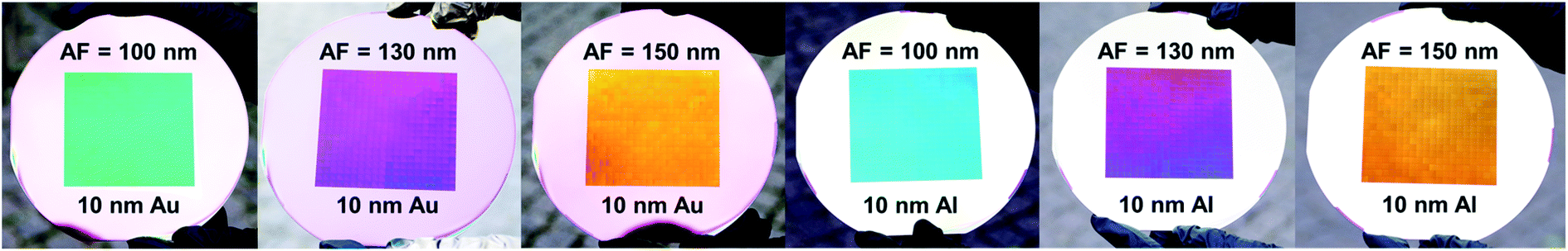 | ||
| Fig. 5 Photographs of large area plasmonic color surfaces taken outdoors, in natural light. The patterned surface areas are 80 × 72 mm2 (∼60 cm2) and are printed on 150 mm silicon wafers. The AF width and metal coating layer is specified on each individual image. | ||
Whereas primary colors were not demonstrated in this paper, it is worth noting that a number of factors influence the reflectance and therefore the color appearance, such as the sizes of the AF employed and the metal chosen for coating. Furthermore, simulation results indicate that further tuning can be achieved by altering the aspect ratio of the structures. Overall, our approach shows excellent flexibility in terms of selecting the color appearance for relatively large plasmonic metasurfaces.
Abbreviations
| LSPR | Localized surface plasmon resonance |
| CD | Critical dimensions |
| EUV | Extreme UV |
| RET | Resolution enhancement technique |
| OAI | Off-axis illumination |
| DUV | Deep UV |
| NA | Numerical aperture |
| DRIE | Deep reactive ion etching |
| DREM | Deposit, remove, etch, multistep |
| BARC | Bottom anti-reflective coating |
| SEM | Scanning electron microscopy |
| EHT | Electron accelerating voltage |
| FEM | Finite element method |
| AF | Assist features |
| AIC | Aerial image contrast |
| NILS | Normalized image log-slope |
| DLCE | Double line cross exposure |
Author contributions
MK – conceptualization, investigation, methodology, writing – original draft; AEW – investigation, methodology, writing – review and editing; KW – investigation, methodology, writing – review and editing; EK – investigation; JU – investigation; AB – funding acquisition, supervision; TR – funding acquisition, supervision; AIB – funding acquisition, supervision, writing – original draft; RJT – conceptualization, funding acquisition, supervision, writing – original draft.Conflicts of interest
There are no conflicts to declare.Acknowledgements
KW, TR and AB acknowledge the IDUN Center of Excellence funded by the Danish National Research Foundation (Project No. DNRF122) and VILLUM FONDEN (Grant No. 9301). AEW acknowledges the Novo Nordisk Foundation (grant number NNF16OC0021948). AIB acknowledges VILLUM FONDEN (grant numbers 34424 and 00022918). MK and RJT acknowledge the PIPSA project under the TIME framework program (Grant No. RFH-18-0017), funded by the EU Regional funding 2014-2020.References
- C. Noguez, J. Phys. Chem. C, 2007, 111, 3806–3819 CrossRef CAS.
- K. S. Lee and M. A. El-Sayed, J. Phys. Chem. B, 2006, 110, 19220–19225 CrossRef CAS.
- H. K. Yu, Y. S. Peng, Y. Yang and Z. Y. Li, npj Comput. Mater., 2019, 5, 45 CrossRef.
- J. R. Mejia-Salazar and O. N. Oliveira, Chem. Rev., 2018, 118, 10617–10625 CrossRef CAS.
- M. J. Kale, T. Avanesian and P. Christopher, ACS Catal., 2014, 4, 116–128 CrossRef CAS.
- E. Engay, A. I. Bunea, M. Chouliara, A. Banas and J. Gluckstad, Opt. Lett., 2018, 43, 3870–3873 CrossRef CAS.
- S. Mallidi, T. Larson, J. Tam, P. P. Joshi, A. Karpiouk, K. Sokolov and S. Emelianov, Nano Lett., 2009, 9, 2825–2831 CrossRef CAS.
- M. W. Song, D. Wang, S. Peana, S. Choudhury, P. Nyga, Z. A. Kudyshev, H. L. Yu, A. Boltasseva, V. M. Shalaev and A. V. Kildishev, Appl. Phys. Rev., 2019, 6, 041308 CAS.
- W. Caseri, Macromol. Rapid Commun., 2000, 21, 705–722 CrossRef CAS.
- A. Kristensen, J. K. W. Yang, S. I. Bozhevolnyi, S. Link, P. Nordlander, N. J. Halas and N. A. Mortensen, Nat. Rev. Mater., 2016, 2, 16088 CrossRef.
- K. Kumar, H. G. Duan, R. S. Hegde, S. C. W. Koh, J. N. Wei and J. K. W. Yang, Nat. Nanotechnol., 2012, 7, 557–561 CrossRef CAS.
- J. S. Clausen, E. Hojlund-Nielsen, A. B. Christiansen, S. Yazdi, M. Grajower, H. Taha, U. Levy, A. Kristensen and N. A. Mortensen, Nano Lett., 2014, 14, 4499–4504 CrossRef CAS.
- X. L. Zhu, C. Vannahme, E. Hojlund-Nielsen, N. A. Mortensen and A. Kristensen, Nat. Nanotechnol., 2016, 11, 325–329 CrossRef CAS.
- S. Murthy, H. Pranov, N. A. Feidenhans'l, J. S. Madsen, P. E. Hansen, H. C. Pedersen and R. Taboryski, Nanoscale, 2017, 9, 14280–14287 RSC.
- B. Luk'yanchuk, N. I. Zheludev, S. A. Maier, N. J. Halas, P. Nordlander, H. Giessen and C. T. Chong, Nat. Mater., 2010, 9, 707–715 CrossRef.
- T. D. James, P. Mulvaney and A. Roberts, Nano Lett., 2016, 16, 3817–3823 CrossRef CAS.
- S. J. Tan, L. Zhang, D. Zhu, X. M. Goh, Y. M. Wang, K. Kumar, C. W. Qiu and J. K. W. Yang, Nano Lett., 2014, 14, 4023–4029 CrossRef CAS.
- H. J. Park, T. Xu, J. Y. Lee, A. Ledbetter and L. J. Guo, ACS Nano, 2011, 5, 7055–7060 CrossRef CAS.
- A. F. Kaplan, T. Xu and L. J. Guo, Appl. Phys. Lett., 2011, 99, 143111 CrossRef.
- Q. J. Wu, H. J. Xia, H. Jia, H. Wang, C. Jiang, L. S. Wang, J. Zhao, R. Z. Tai, S. S. Xiao, D. X. Zhang, S. M. Yang and J. Z. Jiang, Opt. Lett., 2019, 44, 1031–1034 CrossRef CAS.
- Y. S. Do, J. H. Park, B. Y. Hwang, S. M. Lee, B. K. Ju and K. C. Choi, Adv. Opt. Mater., 2013, 1, 133–138 CrossRef.
- J. A. Schuller, E. S. Barnard, W. S. Cai, Y. C. Jun, J. S. White and M. L. Brongersma, Nat. Mater., 2010, 9, 193–204 CrossRef CAS.
- W. L. Barnes, J. Opt. A: Pure Appl. Opt., 2006, 8, S87–S93 CrossRef.
- Y. K. R. Wu, A. E. Hollowell, C. Zhang and L. J. Guo, Sci. Rep., 2013, 3, 1194 CrossRef.
- W. Srituravanich, N. Fang, C. Sun, Q. Luo and X. Zhang, Nano Lett., 2004, 4, 1085–1088 CrossRef CAS.
- S. S. Acimovic, M. P. Kreuzer, M. U. Gonzalez and R. Quidant, ACS Nano, 2009, 3, 1231–1237 CrossRef CAS.
- J. Olson, A. Manjavacas, L. F. Liu, W. S. Chang, B. Foerster, N. S. King, M. W. Knight, P. Nordlander, N. J. Halas and S. Link, Proc. Natl. Acad. Sci. U. S. A., 2014, 111, 14348–14353 CrossRef CAS.
- D. K. Gramotnev and S. I. Bozhevolnyi, Nat. Photonics, 2010, 4, 83–91 CrossRef CAS.
- A. S. Roberts, A. Pors, O. Albrektsen and S. I. Bozhevolnyi, Nano Lett., 2014, 14, 783–787 CrossRef CAS.
- C. U. Hail, G. Schnoering, M. Damak, D. Poulikakos and H. Eghlidi, ACS Nano, 2020, 14, 1783–1791 CrossRef CAS.
- B. Paivanranta, H. Merbold, R. Giannini, L. Buchi, S. Gorelick, C. David, J. F. Loffler, T. Feurer and Y. Ekinci, ACS Nano, 2011, 5, 6374–6382 CrossRef CAS.
- S. H. Ahn and L. J. Guo, Adv. Mater., 2008, 20, 2044–2049 CrossRef CAS.
- S. Murthy, M. Matschuk, Q. Huang, N. K. Mandsberg, N. A. Feidenhans'l, P. Johansen, L. Christensen, H. Pranov, G. Kofod, H. C. Pedersen, O. Hassager and R. Taboryski, Adv. Eng. Mater., 2016, 18, 484–489 CrossRef CAS.
- S. Kasani, K. Curtin and N. Q. Wu, Nanophotonics, 2019, 8, 2065–2089 CAS.
- A. Biswas, I. S. Bayer, A. S. Biris, T. Wang, E. Dervishi and F. Faupel, Adv. Colloid Interface Sci., 2012, 170, 2–27 CrossRef CAS.
- M. Park, C. Harrison, P. M. Chaikin, R. A. Register and D. H. Adamson, Science, 1997, 276, 1401–1404 CrossRef CAS.
- M. Luo and T. H. Epps, Macromolecules, 2013, 46, 7567–7579 CrossRef CAS.
- C. M. Bates, M. J. Maher, D. W. Janes, C. J. Ellison and C. G. Willson, Macromolecules, 2014, 47, 2–12 CrossRef CAS.
- A. Telecka, N. K. Mandsberg, T. Li, E. Ludvigsen, S. Ndoni, R. Di Mundo, F. Palumbo, J. Fiutowski, S. Chiriaev and R. Taboryski, Nanoscale, 2018, 10, 20652–20663 RSC.
- T. Li, Z. L. Wang, L. Schulte, O. Hansen and S. Ndoni, RSC Adv., 2015, 5, 102619–102624 RSC.
- A. Telecka, T. Li, S. Ndoni and R. Taboryski, RSC Adv., 2018, 8, 4204–4213 RSC.
- S. Cataldo, J. Zhao, F. Neubrech, B. Frank, C. J. Zhang, P. V. Braun and H. Giessen, ACS Nano, 2012, 6, 979–985 CrossRef CAS.
- P. Hanarp, D. S. Sutherland, J. Gold and B. Kasemo, Colloids Surf., A, 2003, 214, 23–36 CrossRef CAS.
- D. Y. Xia, Z. Y. Ku, S. C. Lee and S. R. J. Brueck, Adv. Mater., 2011, 23, 147–179 CrossRef CAS.
- T. A. Brunner, J. Vac. Sci. Technol., B: Microelectron. Nanometer Struct.--Process., Meas., Phenom., 2003, 21, 2632–2637 CrossRef CAS.
- R. P. Seisyan, Tech. Phys., 2011, 56, 1061–1073 CrossRef CAS.
- G. M. Wallraff and W. D. Hinsberg, Chem. Rev., 1999, 99, 1801–1821 CrossRef CAS.
- H. J. Levinson, Principles of Lithography, SPIE, Bellingham, Washington 98227-0010, USA, 4th edn, 2019 Search PubMed.
- M. D. Levenson, Jpn. J. Appl. Phys., Part 1, 1994, 33, 6765–6773 CrossRef CAS.
- M. Erdelyi, Z. L. Horvath, G. Szabo, Z. Bor, F. K. Tittel, J. R. Cavallaro and M. C. Smayling, J. Vac. Sci. Technol., B: Microelectron. Nanometer Struct.--Process., Meas., Phenom., 1997, 15, 287–292 CrossRef CAS.
- M. Rothschild, Mater. Today, 2005, 8, 18–24 CrossRef CAS.
- M. Bertalmio, Vision Models for High Dynamic Range and Wide Colour Gamut Imaging: Techniques and Applications, 2020, pp. 131–155 Search PubMed.
- J. Finders, M. Eurlings, K. V. I. Schenau, M. Dusa and P. Jenkins, Proc. SPIE, 2000, 4226 Search PubMed.
- J. Miyazaki and A. Yen, J. Photopolym. Sci. Technol., 2019, 32, 195–201 CrossRef CAS.
- J. Kim, H. Oh, M. Seo and M. Lee, ACS Photonics, 2019, 6, 2342–2349 CrossRef CAS.
- E. Hojlund-Nielsen, T. Greibe, N. A. Mortensen and A. Kristensen, Microelectron. Eng., 2014, 121, 104–107 CrossRef.
Footnote |
| † Electronic supplementary information (ESI) available. See DOI: 10.1039/d0na00934b |
| This journal is © The Royal Society of Chemistry 2021 |