 Open Access Article
Incommensurate transition-metal dichalcogenides via mechanochemical reshuffling of binary precursors†
Ihor Z.
Hlova‡
*a,
Prashant
Singh‡
a,
Serhiy Z.
Malynych
b,
Roman V.
Gamernyk
c,
Oleksandr
Dolotko
a,
Vitalij K.
Pecharsky
ad,
Duane D.
Johnson
 ad,
Raymundo
Arroyave
e,
Arjun K.
Pathak
 f and
Viktor P.
Balema
 *a
*a
aAmes Laboratory, U.S. Department of Energy, Iowa State University, Ames, IA 50011-2416, USA. E-mail: vbalema@ameslab.gov; ihlova@ameslab.gov
bHetman Petro Sahaidachnyi National Army Academy, Lviv, 79026, Ukraine
cIvan Franko National University of Lviv, Lviv, 79005, Ukraine
dDepartment of Materials Science and Engineering, Iowa State University, Ames, IA 50011-1096, USA
eDepartment of Materials Science & Engineering, Texas A&M University, College Station, TX 77843, USA
fDepartment of Physics, SUNY Buffalo State, Buffalo, NY 14222, USA
First published on 7th June 2021
Abstract
A new family of heterostructured transition-metal dichalcogenides (TMDCs) with incommensurate (“misfit”) spatial arrangements of well-defined layers was prepared from structurally dissimilar single-phase 2H-MoS2 and 1T-HfS2 materials. The experimentally observed heterostructuring is energetically favorable over the formation of homogeneous multi-principle element dichalcogenides observed in related dichalcogenide systems of Mo, W, and Ta. The resulting three-dimensional (3D) heterostructures show semiconducting behavior with an indirect band gap around 1 eV, agreeing with values predicted from density functional theory. Results of this joint experimental and theoretical study open new avenues for generating unexplored metal-dichalcogenide heteroassemblies with incommensurate structures and tunable physical properties.
1 Introduction
Layered transition-metal dichalcogenides (TMDCs) with a chemical formula of MX2, where M is a group 4–6 refractory metal and X is a chalcogen (S, Se, or Te), continue to receive much attention as easily accessible sources of single-layer 2D-nanomaterials and building blocks for 3D-heterostructures that demonstrate a broad variety of physical properties suitable for diverse applications.1–7 Generally, heterostructured materials are formed as a result of elaborate syntheses and in minuscule quantities. A versatile synthetic approach enabling simple and reliable preparation of 3D-heterostructured TMDCs in bulk will make those materials broadly available for both fundamental and applied research, potentially revealing new physics and new areas for applications.Bulk TMDCs are built from layers of covalently bonded metal and chalcogen atoms held together via weak van der Waals (vdW) forces (see ESI, Fig. S1†). As a result, they can be easily exfoliated into 2D-nanosheets, even down to single layers.8 Both bulk and 2D-TMDCs demonstrate a broad range of electronic transport properties that span from indirect and direct gap semiconductivity, semimetallic and metallic behavior, to low-temperature superconductivity, depending on the chemical composition and the spatial configurations of the material as well as external stimuli applied.1,9
While binary TMDCs are well known,10 the preparation of layered multi-principal element metal chalcogenides, where different metals (M) and chalcogens (X) share a common crystal lattice, remained challenging until our recent report.11 One of the intriguing outcomes of this earlier study was the observed heterostructuring of different group 5 and 6 binary TMDCs upon mechanical milling at room temperature. Thus-produced 3D-heterostructures are metastable and, when subjected to high-temperature annealing, they transform into uniform single-phase materials. However, if the starting metal chalcogenides possess different crystal structures and stoichiometries, e.g. TaS2 and SmS, or NbSe2 and LaSe, under similar processing conditions they form well-defined and thermodynamically stable heterostructures with incommensurate (misfit) spatial arrangements, where slabs of the mono-chalcogenide (SmS or LaSe) with cubic crystal structures alternate with hexagonal 2D layers of the TMDC (TaS2 or NbSe2).12
The latter discovery raised questions about possibility to design layered misfit materials from chemically related yet structurally dissimilar building blocks, such as hexagonal 2H-MoS2![[thin space (1/6-em)]](https://www.rsc.org/images/entities/char_2009.gif) 13 and trigonal 1T-HfS2,14 by their simultaneous mechanochemical exfoliation and re-assembly into TMDCs heterostructures. If feasible, this would open a new avenue to an unexplored family of incommensurate 3D-heterostructures with tunable physical properties. Below we report on the successful implementation of this idea.
13 and trigonal 1T-HfS2,14 by their simultaneous mechanochemical exfoliation and re-assembly into TMDCs heterostructures. If feasible, this would open a new avenue to an unexplored family of incommensurate 3D-heterostructures with tunable physical properties. Below we report on the successful implementation of this idea.
2 Experimental
2.1 Synthesis of 3D-heterostructures
In a standard experiment, 3 g of a mixture of MoS2 and HfS2 (see ESI, and Fig. S2†) weighed in a desired stoichiometric ratio was loaded in a zirconia vial together with five 12.7 mm zirconia balls. To prevent oxidation. All operations were conducted under the inert atmosphere of an argon-filled glovebox. The sample was milled for 30 hours in a planetary mill (Fritsch, Pulverisette 7) and transferred back to the argon-filled glovebox for loading into a quartz ampule. The ampule was sealed under ultra-high purity helium and the sample was annealed for 3 days at 1000 °C. Thereafter it was cooled down to room temperature and transferred back to the glovebox for further handling.2.2 Powder X-ray diffraction (PXRD)
Phase analyses and structural characterizations of all reactions products were carried out by powder X-ray diffraction (XRD) at room temperature on a PANalytical powder diffractometer using Cu-Kα radiation in the range of Bragg angles 10° ≤ 2θ ≤ 80° with a 0.02° step. Considering lack of periodicity along the stacking direction of a few nanometer thick slabs of the constituent phases, unavoidable and strong texturing, and highly anisotropic peak broadening, Rietveld refinement was impossible. Hence, Le Bail refinements (see ESI and Fig. S3† as an example) of the lattice parameters of the individual phases were performed using FullProf sofware.15 The backgrounds were fitted by linear interpolations between selected data points in the regions with no Bragg peaks present. The pseudo-Voigt function was used to approximate peak shapes, with peak shape parameters refined separately for each of the two phases present.2.3 Scanning transmission electron microscopy (STEM)
High-angle annular dark-field (HAADF) scanning transmission electron microscopy (STEM) and energy dispersive X-ray spectrometry (EDS) experiments were performed on a Titan Themis (FEI) probe Cs-corrected TEM. The high-resolution HAADF-STEM imaging was carried out using a convergence semi-angle of 18 mrad and a collection semi-angle of 99–200 mrad at 200 kV. STEM-EDS analysis was performed using a Super-X EDS detector attached to the Titan Themis.2.4 Band gap measurements
Optical measurements were performed using a custom-built experimental setup (ESI, and Fig. S4† for further details) based on a diffractive monochromator (focal length of the lens 600 mm). A quartz halogen lamp was utilized as a light source and a photomultiplier tube (PMT) was used to detect the radiation. Samples were placed inside the integrating sphere and their diffuse reflectance spectra (DRS) were recorded. Barium sulphate served as a standard. The acquired DRS were converted to Kubelka–Munk function (absorption-to-scattering ratio α/S).2.5 Density functional theory calculations
Density Functional Theory (DFT) calculations were employed as implemented in the Vienna ab initio simulations package (VASP)16–18 with Projector Augmented Wave (PAW) method.19,20 The plane-wave basis cut-off was set at 500 eV, and the k-mesh to sample the first Brillouin zone for geometry optimization and band structure were, respectively, 5 × 5 × 1 and 7 × 7 × 2. Unit-cell translation vectors, cell volumes, and atomic positions were fully optimized in the heterostructures and single-phase solid solution (SS) materials. The convergence criteria for the residual force and energy were set to 10−3 eV Å−1 and 10−5 eV per atom, respectively. The parameter-free van der Waals density functional (optB88-vdW)21 was employed to account for dispersive interactions,22 whereas the hybrid Heyd–Scuseria–Ernzerhof23 functional was employed for band-gap calculations as the van der Waals functionals have a minor effect on the band structure.24 Two main structural configurations that are common for transition-metal dichalcogenides, namely 2H-MX2 and 1T-MX2 polytypes,1 are used to assess the formation energies of different heterostructured and single-phase materials.For DFT calculations of (Mo0.5W0.5)S2 and (Mo0.5W0.5)(S0.5Se0.5)2, we used (I) 24-atom supercell (2 × 2 × 1 unit cells of 2H-MoS2) to mimic disorder, whereas 2H-MoS2 was used to model 1 × 1 × 4 heterostructure supercell. For disorder cases: we use 5 × 5 × 1 and 11 × 11 × 5 k-mesh for structural relaxation and energy. For heterostructures: we use 3 × 3 × 1 and 11 × 11 × 1 k-mesh for structural relaxation and energy. For (Mo40W40Ta20)S2, (II) a 96-atom supercell (4 × 4 × 1 unit cells of 2H-MoS2) was used to mimic disorder, whereas 1 × 1 × 10 supercell of 2H-MoS2 was used to model an ordered 4(TaS2):8(MoS2):8(WS2) heterostructure. For disorder case: we use 5 × 5 × 3 and 8 × 8 × 6 k-mesh for structural relaxation and energy. For heterostructures: we use 3 × 3 × 1 and 9 × 9 × 1 k-mesh for structural relaxation and energy. A manual stacking approach was used to create vertical vdW heterostructures of 2H-MoS2 and 1T-HfS2 in the present study.
3 Results and discussion
3.1 Synthesis and characterization
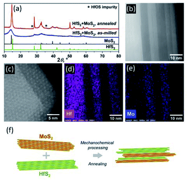
In contrast to the mixtures of binary MX2, where M = Mo, W, Ta, Nb, and X = S or Se, that yield single-phase TMDCs upon mechanical milling and subsequent annealing,11 ball milling of an equimolar mixture of HfS2 and MoS2 in a planetary mill (Fritsch, Pulverisette 7) for 30 hours, followed by a high-temperature annealing at 1000 °C for 72 hours, does not produce a single-phase (Mo0.5Hf0.5)S2. While the X-ray diffraction (XRD) pattern of the as-milled powder consists of several broad peaks characteristic of a highly disordered solid (Fig. 1a), the material obtained after the subsequent annealing is composed of the distinguishable HfS2 and MoS2 phases (Table 1, Fig. 1a).MoS2![[thin space (1/6-em)]](https://www.rsc.org/images/entities/char_2009.gif) : :![[thin space (1/6-em)]](https://www.rsc.org/images/entities/char_2009.gif) HfS2 molar ratio HfS2 molar ratio |
MoS2 (2H) lattice parametersb (Å) | HfS2 (1T) lattice parametersc (Å) | R p, % |
|---|---|---|---|
a The Rp values correspond to the profile residuals.
b Space group symmetry P63/mmc (#194).
c Space group symmetry P![[3 with combining macron]](https://www.rsc.org/images/entities/char_0033_0304.gif) m1 (#164).
d Processed twice using the same synthesis protocol as the previous material. m1 (#164).
d Processed twice using the same synthesis protocol as the previous material.
|
|||
1![[thin space (1/6-em)]](https://www.rsc.org/images/entities/char_2009.gif) : :![[thin space (1/6-em)]](https://www.rsc.org/images/entities/char_2009.gif) 0 0 |
a = 3.160(1) Å | — | 6.07 |
| c = 12.298(2) Å | |||
0.75![[thin space (1/6-em)]](https://www.rsc.org/images/entities/char_2009.gif) : :![[thin space (1/6-em)]](https://www.rsc.org/images/entities/char_2009.gif) 0.25 0.25 |
a = 3.157(1) Å | a = 3.626(1) Å | 7.83 |
| c = 12.286(1) Å | c = 5.852(1) Å | ||
0.5![[thin space (1/6-em)]](https://www.rsc.org/images/entities/char_2009.gif) : :![[thin space (1/6-em)]](https://www.rsc.org/images/entities/char_2009.gif) 0.5 0.5 |
a = 3.162(1) Å | a = 3.634(1) Å | 7.68 |
| c = 12.124(1) Å | c = 5.880(1) Å | ||
0.5![[thin space (1/6-em)]](https://www.rsc.org/images/entities/char_2009.gif) : :![[thin space (1/6-em)]](https://www.rsc.org/images/entities/char_2009.gif) 0.5d 0.5d |
a = 3.159(1) Å | a = 3.629(1) Å | 6.01 |
| c = 12.074(1) Å | c = 5.881(1) Å | ||
0.25![[thin space (1/6-em)]](https://www.rsc.org/images/entities/char_2009.gif) : :![[thin space (1/6-em)]](https://www.rsc.org/images/entities/char_2009.gif) 0.75 0.75 |
a = 3.163(1) Å | a = 3.634(1) Å | 6.52 |
| c = 12.255(1) Å | c = 5.951(1) Å | ||
0![[thin space (1/6-em)]](https://www.rsc.org/images/entities/char_2009.gif) : :![[thin space (1/6-em)]](https://www.rsc.org/images/entities/char_2009.gif) 1 1 |
— | a = 3.628(1) Å | 9.88 |
| c = 5.854(1) Å | |||
Lattice parameters of both TMDC phases in the annealed sample reveal a slight reduction (∼1.4%) of the parameter c in the MoS2 phase and a smaller but noticeable expansion (∼0.5%) of the parameter c in the HfS2 constituent. Considering that rMo = 1.400 Å < rHf = 1.580 Å (metallic radii for coordination number 12), these anomalies cannot be attributed to minor substitutions on the metal sites. The changes that occur in opposite direction are not likely to be related to various concentrations of defects in two different structural motifs and, therefore, we ascribe them to large errors that arise from a number of factors. These are: strong diffuse scattering due to a few-nanometer thick slabs stacked along the c direction (see Fig. 1b–e); heavy overlap of the majority of the strongest Bragg peaks; and highly anisotropic broadening due to epitaxial strains that are unavoidable and cannot be removed by annealing. All of them combined, Le-Bail-refined unit-cell dimensions, and in particular those parallel to the stacking direction, become susceptible to random errors, even though the formal least squares standard deviations listed in Table 1 are low.
A minor impurity detected in the annealed sample almost certainly belongs to an off-stoichiometric hafnium oxysulfide that has formed in the sample even though all operations were carried out under high-purity argon or helium. The annealed material was further studied using High-Angle Annular Dark Field Scanning Transmission Electron Microscopy (HAADF-STEM) and Energy Dispersive Spectroscopy (STEM-EDS), which reveal a well-defined sandwich-like arrangement of the separate phases in the material as shown in Fig. 1b. The alternating phases have different Z-contrast, whereby the MoS2 slabs appear dark and HfS2 produces much brighter segments. The thickness of specific slabs varies, indicating stochastic nature of the mechanical exfoliation and self-assembly processes. Furthermore, the HAADF-STEM images reveal the presence of the Moiré pattern on the surface of the material (Fig. 1c), which is characteristic for TMDCs with lattice mismatch layers positioned on the top of each other,25i.e. incommensurate structural arrangements. STEM-EDS (Fig. 1d, e) confirms the 3D-heterostructured arrangement of the layers in the sample. The schematic diagram illustrating the formation of 3D-heterostructured TMDCs is shown in Fig. 1f.
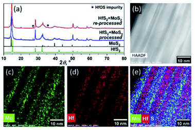
Reprocessing of the annealed material by its milling for additional 30 hours, followed by annealing at 1000 °C for 72 hours, does not eliminate the phase separation in the sample. Its XRD, HAADF-STEM and STEM-EDS analyses clearly indicate that the sandwich-like arrangement of the MoS2 and HfS2 slabs is retained in the reprocessed material (Fig. 2, Table 1), although the slabs become markedly thinner.
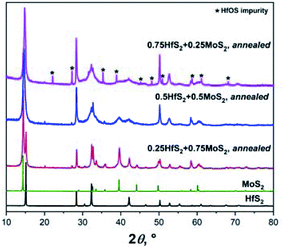
Two other MoS2-HfS2 compositions that are rich in one or another component were prepared and investigated as well.
The XRD patterns and the structural parameters of the obtained samples are shown in Fig. 3 and Table 1. Also, in these cases, a distinctive formation of solid solutions could not be detected. The increased fraction of the HfOS impurity seen in the XRD pattern of Hf0.75Mo0.25S2 correlates with increased concentration of Hf in the material and indicates higher sensitivity of the Hf-rich material to oxygen. As discussed above, minor non-systematic changes in the c lattice parameters are related to contributions from diffuse scattering and varying anisotropic peak broadening.
3.2 Density functional theory calculations
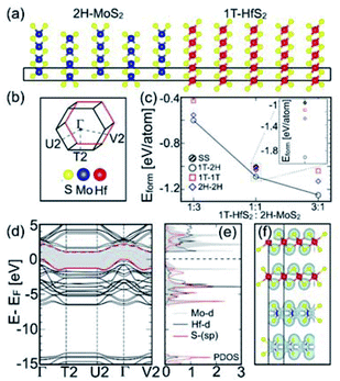
To gain initial insight into different chemical behaviours of structurally similar group 4, 5 and 6 TMDCs, we analysed phase stability, nature of band gap, and electronic structure calculated from DFT.The formation energies (Eform) calculated for equimolar. (5![[thin space (1/6-em)]](https://www.rsc.org/images/entities/char_2009.gif) :
:![[thin space (1/6-em)]](https://www.rsc.org/images/entities/char_2009.gif) 5) HfS2/MoS2 heterostructures and the solid-solution (SS) compound are shown in Fig. 4c. Their comparison indicates that the 5(1T-HfS2)/5(2H-MoS2) arrangement is the most stable among evaluated structures, as its Eform is as low as −1.0902 eV per atom [which is 59.92, 73.45, and 84.32 meV below the Eform calculated, respectively, for 5(1T-HfS2)/5(1T-MoS2), 5(2H-HfS2)/5(2H-MoS2), and SS-(Mo0.5Hf0.5)S2].
5) HfS2/MoS2 heterostructures and the solid-solution (SS) compound are shown in Fig. 4c. Their comparison indicates that the 5(1T-HfS2)/5(2H-MoS2) arrangement is the most stable among evaluated structures, as its Eform is as low as −1.0902 eV per atom [which is 59.92, 73.45, and 84.32 meV below the Eform calculated, respectively, for 5(1T-HfS2)/5(1T-MoS2), 5(2H-HfS2)/5(2H-MoS2), and SS-(Mo0.5Hf0.5)S2].
In addition, two other families of x5HfS2/y5MoS2 materials were investigated. Their unit cells were built from five-layer HfS2 and MoS2 slabs taken in 1![[thin space (1/6-em)]](https://www.rsc.org/images/entities/char_2009.gif) :
:![[thin space (1/6-em)]](https://www.rsc.org/images/entities/char_2009.gif) 3 (x = 1, y = 3) and 3
3 (x = 1, y = 3) and 3![[thin space (1/6-em)]](https://www.rsc.org/images/entities/char_2009.gif) :
:![[thin space (1/6-em)]](https://www.rsc.org/images/entities/char_2009.gif) 1 (x = 3, y = 1) stoichiometric proportions or SS, (MoyHfx)S2, layers. The calculated Eform values are plotted in Fig. 4c. Here, we also find that the x5(1T-HfS2)/y5(2H-MoS2) heterostructural arrangements are the most energy favorable among other evaluated cases. We also investigated several other possibilities, for example, solubility of Hf in 2H-MoS2 or Mo in 1T-HfS2 or anti-site defects (Mo and Hf at the interface were interchanged to see the effects on energetics), vacancies (Mo or Hf or S). However, none of these possibilities are thermodynamically stable compared to pure 2H-MoS2-1T-HfS2 interface.
1 (x = 3, y = 1) stoichiometric proportions or SS, (MoyHfx)S2, layers. The calculated Eform values are plotted in Fig. 4c. Here, we also find that the x5(1T-HfS2)/y5(2H-MoS2) heterostructural arrangements are the most energy favorable among other evaluated cases. We also investigated several other possibilities, for example, solubility of Hf in 2H-MoS2 or Mo in 1T-HfS2 or anti-site defects (Mo and Hf at the interface were interchanged to see the effects on energetics), vacancies (Mo or Hf or S). However, none of these possibilities are thermodynamically stable compared to pure 2H-MoS2-1T-HfS2 interface.
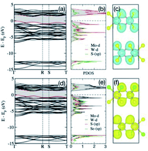
The calculated partial density of states (DOS) and the charge-density for 5(1T-HfS2)/5(2H-MoS2) heterostructures, and the Mo-d, Hf-d, and S-sp bands are shown in Fig. 4d–f. The bands near the Fermi energy (EF in Fig. 4d-e) mainly consist of the S-p states that are hybridized with the Mo-d and Hf-d states, whereas the S-s orbitals emerge way below EF, and are separated from the other valence states by 8.0 eV, i.e., are chemically inactive. The strong intralayer hybridization between the d-orbitals of Mo and Hf, and the p-orbitals of S is also evident from the overlapping charge densities shown in Fig. 4f, which stabilizes the 5(1T-HfS2)/5(2H-MoS2) heterostructure. The charge density in both 1T-HfS2 and 2H-MoS2 layers is localized on the S atoms with the directional intralayer bonding toward Mo and Hf and the band gap of 1.01 eV.
The calculated band gaps for (Mo0.5W0.5)S2 and (Mo0.5W0.5)SSe are 1.02 eV and 1.17 eV, respectively. They are indirect in nature and follow the Γ–R high-symmetry direction. Surprisingly, the effect of Se-substitution is quite moderate in this case.
Finally, we also evaluated the formation energies and electronic structures of the single-phase material with the nominal composition of (Mo0.4W0.4Ta0.2)S2. Partial replacement of Mo and W by Ta in (Mo0.5W0.5)S2 can be seen as an injection of 0.2 holes per molecule into the system. Once again, the calculated Eform of the “hole-doped” (Mo0.4W0.4Ta0.2)S2 is substantially lower than that of the heterostructure material (−0.875 vs. −0.835 eV per atom), which explains the experimentally observed formation of the solid-solution phase in this case.11
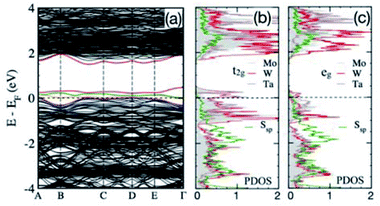
The band structure and partial DOS for (Mo0.4W0.4Ta0.2)S2 are shown in Fig. 6. The presence of Ta is responsible for only a partial filling of bonding Mo/W d-states, while they are completely filled in (Mo0.5W0.5)S2 (Fig. 5a and b). This moves the bonding t2g and eg states (Fig. 6b and c) to EF, where the majority of states belong to Mo/W/Ta t2g-bands. Here, t2g is a combination of dxy, dyz, and dxz orbitals and eg represents dx2y2 and dz2 orbitals. The S p-bands near EF are situated in the same energy range as the Mo/W d-bands in (Mo0.5W0.5)S2 (Fig. 5b), and Ta causes reduced filling of S p-bands that also move closer to EF. Thus, the crossover of partially-filled Mo/W-d and S-p bands at EF caused by Ta predicts metallic behaviour of (Mo0.4W0.4Ta0.2)S2.
In summary, our DFT results reveal that combining structurally different 1T-HfS2 and 2H-MoS2 phases stabilizes the heterostructured arrangement over solid-solution-like single-phase (1T or 2H) states. At the same time, blending isostructural TMDCs, such as 2H-MoX2 and 2H-WX2 (X = S, Se), produces single-phase materials; even so, the metastable heterostructured intermediates are observed after the low-temperature stages of the previous experiments.11 Doping group 6 TMDCs with a group 5 metal (Ta) is not expected to affect the phase stability of the resulting compounds, but it changes transport behaviour from semiconducting to metallic.
3.3 Electronic transport measurements
Electronic transport of the equimolar HfS2/MoS2 heterostructure and some previously prepared multi-principal element, single-phase TMDCs,11 have been studied using photoconductivity, optical band gap, and electrical resistivity measurements. The experimental band gap values along with those predicted by the DFT calculations are summarized in Table 2, together with those reported in the literature.The additional experimental details on measurements performed can be found in the ESI.† Several observations are worth noting. First, in the majority of the cases, the experimental values are in a good agreement with those predicted by DFT or published in the literature. The band gap values experimentally determined for both the HfS2/MoS2 and the multi-principal elements TMDCs shown in Table 2 are below those observed in the pure binary precursors, and obviously can be fine-tuned by altering the material's chemical and phase compositions.
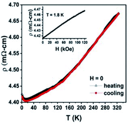
The electronic transport behaviour of multi-principal element TMDCs can be further manipulated by doping with group 5 transition metals, such as Ta, that converts them from semiconductors into metallic-type conductors.30 To illustrate this, we measured temperature dependence of the electrical resistivity, ρ(T), of W0.4Mo0.4Ta0.2S2 using a Physical Property Measurements System (PPMS, Quantum Design, Inc.) employing a standard four-probe technique in magnetic field up to 120 kOe. The ρ vs. (T) measured during cooling and heating between 320 K and 1.8 K in the absence of magnetic field (H = 0) is shown in Fig. 7. Both the heating and cooling curves are practically identical. Consistent with the theoretical prediction, W0.4Mo0.4Ta0.2S2 demonstrates a weakly temperature-dependent metallic conductivity between 300 and 14 K. A minor increase in the resistivity observed at T ≤ 14 K can be attributed to the presence of electron transport barriers between crystallites in the sample that reduce its overall conductivity at cryogenic temperatures. The electrical resistivity measured as a function of the magnetic field up to 120 kOe (Fig. 7, inset) indicates very weak but positive magnetoresistance of ∼1.2% at T = 1.8 K without any sign of saturation.
4 Conclusions
In contrast to the group 5 and 6 TMDCs, HfS2 does not form a solid solution with MoS2 after prolonged mechanical milling and annealing, even if they are performed in a cyclic manner. The misfit 3D-heterostructures formed from 1T-HfS2 and 2H-MoS2 building blocks show semiconducting behaviour with indirect band gap around 1 eV, which agrees well with the value predicted by DFT calculations and is lower than the values reported for the pure binary precursor materials. Our results also demonstrate that electronic transport in bulk TMDCs can be successfully manipulated using doping with appropriate refractory metals, which opens new avenues for engineering of vdW materials with tuneable physical properties.Author contributions
I. Z. H., O. D. contributed to design of experiments, performed materials synthesis, materials characterization and contributed to interpretation of results; O. D. performed Rietveld refinements; S. Z. M., R. V. G and A. K. P. performed electronic transport experiments and data interpretation; V. K. P. contributed to structural data interpretation; P. S. and D. D. J. performed DFT calculations and analysis; V. P. B. conceived the idea, supervised and guided the study, contributed to design of experiments and data interpretation. All authors provided comments and edits during the preparation of the manuscript.Conflicts of interest
There are no conflicts to declare.Acknowledgements
The materials development was supported by the Ames Laboratory's Laboratory Directed Research and Development (LDRD) program. Theoretical design & analysis, structural and physical property characterization efforts were supported by the U.S. Department of Energy (DOE) Office of Science, Basic Energy Sciences, Materials Science & Engineering Division. Ames Laboratory is operated for the U.S. DOE by Iowa State University of Science and Technology under Contract No. DE-AC02-07CH11358. Theoretical calculations were conducted using the advanced computing resources provided by Texas A&M High-Performance Research Computing.Notes and references
- A. V. Kolobov and J. Tominaga, Two-Dimensional Transition-Metal Dichalcogenides, Springer International Publishing, Switzerland, 2016 Search PubMed.
- A. K. Geim and I. V. Grigorieva, Nature, 2013, 499, 419–425 Search PubMed.
- K. S. Novoselov, A. Mishchenko, A. Carvalho and A. H. Castro Neto, Science, 2016, 353, aac9439 Search PubMed.
- V. S. Pervov and E. V. Makhonina, Russ. Chem. Rev., 2000, 69, 481–489 Search PubMed.
- M. Serra and R. Tenne, J. Coord. Chem., 2018, 71, 1669–1678 Search PubMed.
- H. Taghinejad, M. Taghinejad, A. A. Eftekhar, Z. Li, M. P. West, M. H. Javani, S. Abdollahramezani, X. Zhang, M. Tian, T. Johnson-Averette, P. M. Ajayan, E. M. Vogel, S.-F. Shi, W. Cai and A. Adibi, ACS Nano, 2020, 14, 6323–6330 Search PubMed.
- J. Joshi, T. Zhou, S. Krylyuk, A. V. Davydov, I. Žutić and P. M. Vora, ACS Nano, 2020, 14, 8528–8538 Search PubMed.
- J. R. Brent, N. Savjani and P. O'Brien, Prog. Mater. Sci., 2017, 89, 411–478 Search PubMed.
- F. Lacopi, J. J. Boeckl and C. Jagadish, Semiconductors and Semimetals. v. 95, 2D Materials, Academic Press, Cambridge, San Diego, Oxford, London, 2016 Search PubMed.
- F. A. Cotton, G. Wilkinson, C. A. Murillo, M. Bochmann and R. Grimes, Advanced Inorganic Chemistry, Wiley, New York, 5th edn, 1988 Search PubMed.
- I. Z. Hlova, O. Dolotko, B. W. Boote, A. K. Pathak, E. A. Smith, V. K. Pecharsky and V. P. Balema, Chem. Commun., 2018, 54, 12574–12577 Search PubMed.
- O. Dolotko, I. Z. Hlova, A. K. Pathak, Y. Mudryk, V. K. Pecharsky, P. Singh, D. D. Johnson, B. W. Boote, J. Li, E. A. Smith, S. L. Carnahan, A. J. Rossini, L. Zhou, E. M. Eastman and V. P. Balema, Nat. Commun., 2020, 11, 1–10 Search PubMed.
- I. Song, C. Park and H. C. Choi, RSC Adv., 2015, 5, 7495–7514 Search PubMed.
- L. F. Mattheiss, Phys. Rev. B: Condens. Matter Mater. Phys., 1973, 8, 3719 Search PubMed.
- T. Roisnel and J. Rodriguez-Carvajal, Mater. Sci. Forum, 2001, 378, 118–123 Search PubMed.
- G. Kresse and J. Furthmüller, Phys. Rev. B: Condens. Matter Mater. Phys., 1996, 54, 11169–11186 Search PubMed.
- G. Kresse and J. Furthmüller, Comp. Mater. Sci, 1996, 6, 15 Search PubMed.
- J. P. Perdew, K. Burke and M. Ernzerhof, Phys. Rev. Lett., 1996, 77, 3865–3868 Search PubMed.
- P. E. Blochl, Phys. Rev. B: Condens. Matter Mater. Phys., 1994, 50, 17953–17979 Search PubMed.
- G. Kresse and D. Joubert, Phys. Rev. B: Condens. Matter Mater. Phys., 1999, 59, 1758–1775 Search PubMed.
- G. Roman-Perez and J. M. Soler, Phys. Rev. Lett., 2009, 103, 096102 Search PubMed.
- J. Klimes, D. R. Bowler and A. Michaelides, Phys. Rev. B: Condens. Matter Mater. Phys., 2011, 83, 195131 Search PubMed.
- J. Heyd, G. E. Scuseria and M. Ernzerhof, J. Chem. Phys., 2006, 124, 219906 Search PubMed.
- Z.-X. Hu, H. P. Lan and W. Ji, Sci. Rep., 2014, 4, 5036 Search PubMed.
- A. B. Naden, K. J. O'Shea and D. A. MacLaren, Nanotechnology, 2018, 29, 165704 Search PubMed.
- K. Kobayashi and J. Yamauchi, Phys. Rev. B: Condens. Matter Mater. Phys., 1995, 51, 17085 Search PubMed.
- K. Terashima and I. Imai, Solid State Commun., 1987, 63, 315–318 Search PubMed.
- R. Coehoorn, C. Haas and R. de Groot R, Phys. Rev. B: Condens. Matter Mater. Phys., 1987, 35, 6203–6206 Search PubMed.
- A. Prakash and J. Appenzeller, ACS Nano, 2017, 11, 1626–1632 Search PubMed.
- V. P. Balema, S. Padalkar, I. Z. Hlova, T. Lan, O. Dolotko, V. K. Pecharsky, D. D. Johnson, A. Pathak and P. Singh, U.S. Pat. Appl. Publ., 2020, US 20200109479 A1 20200409 Search PubMed.
Footnotes |
| † Electronic supplementary information (ESI) available: Additional experimental details on precursor synthesis, Rietveld refinement, photoconductivity and magnetoresistance measurements, and density functional theory calculations. See DOI: 10.1039/d1na00064k |
| ‡ These authors contributed equally. |
| This journal is © The Royal Society of Chemistry 2021 |

