 Open Access Article
Robust charge spatial separation and linearly tunable band gap of low-energy tube-edge phosphorene nanoribbon†
Mingyue
Xia
a,
Hongsheng
Liu
 a,
Lu
Wang
 b,
ShiQi
Li
a,
Junfeng
Gao
 *a,
Yan
Su
 *a and
Jijun
Zhao
a
aKey Laboratory of Material Modification by Laser, Ion and Electron Beams (Dalian University of Technology), Ministry of Education, Dalian, 116024, China. E-mail: gaojf@dlut.edu.cn; su.yan@dlut.edu.cn
bInstitute of Functional Nano & Soft Materials (FUNSOM), Jiangsu Key Laboratory for Carbon-Based Functional Materials & Devices, Soochow University, Suzhou, Jiangsu 215123, China
First published on 31st May 2021
Abstract
Versatile applications have been proposed for phosphorene nanoribbons (PNRs), whose properties depend strongly on the edge structures. Recently, a unique tube-reconstruction at the zigzag edge (ZZ[Tube]) of PNRs was discovered to be the lowest configuration. Therefore, studies on PNRs should be reconsidered. In this paper, we systemically explore the width and strain effects on zigzag PNRs with different edge structures, including ZZ[Tube], ZZ and ZZ[ad] edges. ZZ PNRs always have small band gaps which are nearly independent of both width and strain. A remarkable band gap exists in ZZ[ad] PNRs which increases with a decrease in the ribbon width but is not sensitive to strain. In contrast, the band gaps of ZZ[Tube] PNRs change from 1.08 to 0.70 eV as the width increases from 12 to 65 Å. In addition, the band gaps of ZZ[Tube] PNRs show a linear response under a certain range of strain. In addition, the carrier effective masses (0.50 m0 for electrons and 0.94 m0 for holes) of ZZ[Tube] PNRs are much lower than for ZZ[ad], and the VBM and CBM charges are robustly spatially separated even under strains ranging from −5% to 5%. Their ease of formation, lowest energy, light effective mass, linear band gap response to strain and robust charge spatial separation provide ZZ[Tube] PNRs with potentially excellent performance in microelectronic and opto-electric applications.
Introduction
Phosphorene not only has high carrier mobilities,1 but also has a suitable band gap with a high on/off switching ratio (102 to 105).1–8 It fills in the gap between graphene (very high mobility and low on/off ratio) and transition metal dichalcogenides (low mobility and very high on/off ratio).9–12 In addition, phosphorene has strongly anisotropic behavior.2,13–17 As a consequence, phosphorene is proposed as a superior candidate for future fast nanoelectronic devices.The two most important factors are edge and width for nanoribbons, which are common structures for 2D material applications.18–21 Firstly, the properties of nanoribbons depend strongly on edge structures, which may possess remarkable edge states.22,23 Indeed, versatile applications based on the properties of phosphorene nanoribbon edges have been predicted, such as topological edge states accommodated in the quasi-flat band,24 unique shuttle-shaped edge bands,25 and highly efficient solar cell by edge modifications.26
However, a remarkable edge state is likely to be passivated by edge reconstruction. For example, a graphene zigzag (ZZ) edge can easily form 5|7 reconstructions,27–31 and MoS2 ZZ edges undergo special (2 × 1) and (3 × 1) reconstructions.32 Early theoretical calculations showed that pristine ZZ phosphorene nanoribbons (PNRs) are metallic.33,34 However, scanning tunneling microscopy (STM) suggests that ZZ PNRs are semiconductors with a remarkable band gap,35 indicating that an edge reconstruction may exist. A relaxed pristine zigzag edge with a charge density wave (CDW) (called the ZZ-edge here) is semiconducting, but its band gap is only 0.1 eV, or even smaller.36 A Klein-edge with a (2 × 1) reconstruction (named the ZZ[ad]-edge in this paper) was later proposed to be more stable, but its edge state is above the Fermi level, unlike the experimental finding where the edge state is below Fermi level.31,36
Previously, there was an attempt to assemble a 1D carbon nanotube with graphene nanoribbon to introduce van Hove singularities.37 Interestingly, the zigzag edge of black phosphorene can self-reconstruct into an ultimate narrow phosphorene nanotube, spontaneously assembling a 1D phosphorene nanotube with nanoribbon.36 It was found that such a tubed edge is the lowest edge configuration. In addition, a ZZ[Tube] PNR with 4 nm width has a remarkable band gap of 1.23 eV, and the edge state is below the Fermi level, agreeing with the experiments very well.35,36 Further studies indicate that the tube-reconstruction can also change the thermal vibration and thermal transport of PNRs.38–42 Therefore, ZZ[Tube] certainly remarkably alters the properties of the PNR, and the proposed applications based on the tube edge should be further explored.
A second important factor is that the properties of nanoribbons vary with width due to the quantum confinement effect. For example, the band gap of armchair graphene nanoribbons follows a 3p + 2 rule.27,43 MoS2 nanoribbons44 and armchair h-BN nanoribbons45 also exhibit oscillating band gaps with a variation in ribbon width. In addition, the band gap of semiconducting graphene nanoribbons46 decreases monotonically with an increase in the ribbon width. In addition to the edge state and width, strain engineering is also an effective method of tuning the properties of nanoribbons.41,47 The band gaps of armchair MoS2 (ref. 48) and zigzag h-BN49 nanoribbons decrease with increasing strain. Therefore, we can infer that width and strain certainly affect the properties of reconstructed ZZ[Tube] PNRs. However, to the best of our knowledge, the width and strain effects on the ZZ[Tube] PNRs have not been studied, which is significant for applications.
In this paper, using density functional theory (DFT) calculations, we compare the effects of ribbon width and strain on the electronic properties of PNRs, including ZZ, ZZ[ad] and ZZ[Tube]. Our results show that the behaviors of ZZ[Tube] PNRs are very different from those of ZZ and ZZ[ad] PNRs. The band gap of ZZ[Tube] PNRs can be effectively tuned by both width and strain. In addition, ZZ[Tube] PNRs exhibit unique and robust charge spatial separation of the valence band maximum (VBM) and conduction band minimum (CBM) under −5% to 4% strain. Robust spatial charge separation and the tunable band gap of ZZ[Tube] PNRs suggest their potential applications in microelectronics and opto-electronics.
Results and discussion
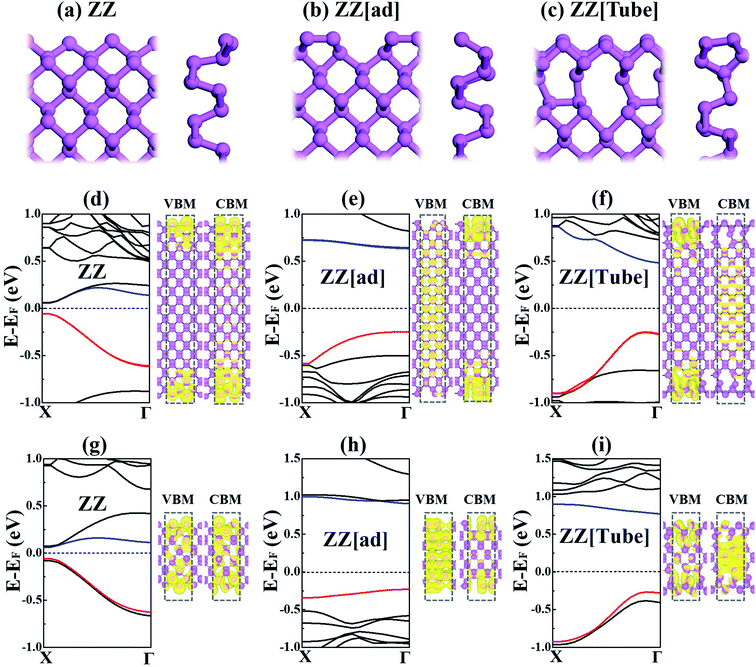
Our calculations50,51 were carried out with the Vienna Ab-initio Simulation Package (VASP), using the planewave basis with a carefully tested energy cutoff of 460 eV. Details of the computational method can be found in the ESI.† ZZ[Tube] is the lowest edge,35,36 while ZZ and ZZ[ad] were the most explored. Therefore, here only PNRs with ZZ, ZZ[ad] and ZZ[Tube] edges are compared, as shown in Fig. 1a–c. For each kind of PNR, the ribbon can be either symmetric or asymmetric, depending on the orientation of the two edges. We find the properties of PNRs are nearly independent of the orientation of the edge; therefore for simplicity only the results with asymmetric edges are presented in the manuscript. All the results for PNRs with symmetric edges can be found in Fig. S1–S4 in the ESI.†The band structures for ZZ, ZZ[ad] and ZZ[Tube] PNRs with 40 Å width are shown in Fig. 1d–f. All three PNRs are semiconductors with band gaps of 0.13, 0.88 and 0.73 eV for ZZ, ZZ[ad] and ZZ[Tube], respectively. These agree well with previous research.35,36 However, essential differences exist in the band structures, which can be understood via the charge of the valence band maximum (VBM) and the conduction band bottom (CBM) shown in Fig. 1d–f. For ZZ PNR, both VBM and CBM are contributed by edge states. For ZZ[ad] PNR, the VBM is mainly contributed by bulk states and the CBM is contributed by edge states. In contrast, for ZZ[Tube] PNR, the VBM is contributed by edge states and the CBM is contributed by bulk states.
In addition, the carrier effective masses at the CBM and VBM of ZZ[Tube] PNR (0.42 m0 for electrons and 1.24 m0 for holes) are much smaller than for ZZ[ad] PNR (9.06 m0 for electrons and 8.80 m0 for holes) due to the larger dispersion of the bands. Therefore, a large carrier mobility can be expected in ZZ[Tube] PNR, which is important for applications in electronic devices. ZZ PNR has comparable carrier effective masses (0.50 m0 for electrons and 0.94 m0 for holes) to those of ZZ[Tube] PNR but it is much less stable. Therefore, edge reconstruction can significantly alter the nature of the electronic structure.
We further roughly checked the width effect by comparing calculations of the electronic structures of PNRs with a ribbon width of 15 Å (Fig. 1g–i). For ZZ PNR, the VBM does not change much and the CBM shifts downwards except for the value at the X point. Therefore, the band gap of ZZ PNR changes slightly (from 0.13 eV to 0.12 eV). In contrast, the band gaps of ZZ[ad] and ZZ[Tube] PNRs increase by 0.30 eV and 0.26 eV when the width changes from 40 Å to 15 Å. Due to the quantum confinement effect, the width also alters the nature of the VBM and CBM, which can be visualized by charge density plotting, as shown beside each band structure.
Our band structure calculations in this paper are based on the standard PBE exchange–correlation functional, which may underestimate the band gap. Hybrid functionals or GW calculations can give more accurate band gaps.35,52,53 For example, the band gap of 43 Å ZZ[Tube] PNR is 0.63 eV based on PBE, while it is 1.23 eV using HSE06.36 However, the band alignment and dispersion curvature are quite similar for both PBE and HSE06. In addition, both PBE and HSE06 exhibit the same charge separation of VBM and CBM for PNR with a tube edge.36 A previous study also found that the standard PBE can give the correct trend of the band gap changing from monolayer to bulk, compared with GW results.36,54,55 This paper aims to reveal the width and strain influence on PNRs with different edges. Standard PBE can give a suitable band gap changing trend and reveal the charge separation of VBM and CBM. The computational cost is huge even using standard PBE, therefore, we cannot afford the much more costly HSE06 and GW methods for this in-time work. However, the more accurate electronic properties of ZZ[Tube] PNR based on HSE06 and GW are highly deserving of future study.
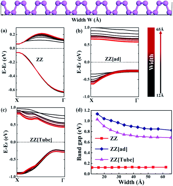
As discussed above, the ribbon width, whose definition is schematically shown in Fig. 2, has a significant influence on the electronic structure of PNRs. Therefore, the changes in VBM and CBM with width ranging from 15 Å to 65 Å for three kinds of PNRs are plotted in Fig. 2a–c. For ZZ PNRs, the VBM does not change with the ribbon width and the CBM shifts upwards with an increase in the width but keeping the X point fixed. Thus, the band gap of ZZ PNRs is not sensitive to the ribbon width (red line in Fig. 2d). For ZZ[ad] PNRs, the VBM at the Γ point changes slightly with the ribbon width, but the CBM drops a lot with an increase in the width, resulting in a decreasing gap with increasing width (blue line in Fig. 2d).
In contrast, for ZZ[Tube] PNRs, the CBM drops a lot with an increase in width. As a consequence, the band gap of ZZ[Tube] PNRs decreases from 1.03 to 0.69 eV with an increase in width (pink line in Fig. 2d). As shown in Fig. 2d, when the width is greater than 40 Å, the band gap does not change much any more with width for all three kinds of PNRs, implying the weakness of the quantum confinement effect in very wide nanoribbons. The full band structures of ZZ, ZZ[ad] and ZZ[Tube] PNRs with different widths can be seen in Fig. S1, S2 and S3,† respectively.
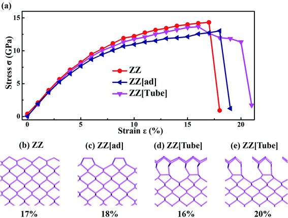
Strain engineering is also a simple and effective method of tuning the properties of nanoribbons. We studied the yield stress for the three PNRs to check the strain limit before their impact on electronic properties. As discussed above, we chose 40 Å wide PNRs to weaken the width effect and focused on the strain effect, as shown in Fig. 3a (strain–stress curves for PNRs with different widths are shown in Fig. S4 in the ESI†). For ZZ PNR, under a critical strain of 17%, the stress drops abruptly giving a yield stress of 14.32 GPa. The yield is due to the structural change with bond rotation, as shown in Fig. 3b. A similar structural change occurs in ZZ[ad] PNR under a critical strain of 18% (Fig. 3c) resulting in a yield stress of 13.03 GPa (Fig. 3a).
In sharp contrast, there are two critical points for ZZ[Tube] PNR, i.e. 16% and 20%. When the strain reaches 16%, partial chemical bonds at the edges break, leading to a slight drop in stress. Then the stress slowly decreases with increasing strain, keeping the geometry of the middle part of the ribbon the same as that in bulk phosphorene. When the strain reaches 20%, a similar structural change occurs to that in ZZ PNRs, resulting in a sharp drop in the stress and a yield stress of 11.33 GPa. Therefore, compared with ZZ and ZZ[ad] PNRs, ZZ[Tube] PNR has a smaller yield stress and stronger flexibility. The detailed structural deformation of ZZ, ZZ[Tube] and ZZ[ad] PNRs during stretching can be found in Fig. S5 in the ESI.† All three edge reconstructed PNRs have stronger flexibility compared with unconstructed PNRs.47
The above mechanical properties are the ideal mechanical properties of PNRs using an adiabatic approximation. The results are only correct at very low temperature. Under common conditions, temperature may seriously affect the fracture behavior. To verify its stability, we performed AIMD for ZZ[Tube] PNRs under 4% strain (Fig. S6†). The temperature is around 300 K. After 9 ps simulations, the ZZ[Tube] PNRs are completely retained. We then further simulated PNR with ZZ[Tube] under 15% (Fig. S6b†), 16% (Fig. S6c†) and 17% (Fig. S6d†) strains at T = 300 K through AIMD. After 5 ps simulations, the structure is still very stable under 15% (Fig. S6b†) and 16% (Fig. S6c†) strain. Under 17% strain, the tube edges are broken, while the inner phosphorene is still stable. These results are the same as those for structural relaxation, meaning that PNR under 17% strain is not broken. This is similar to previous studies, which indicate that PNR can afford a large strain in the ZZ direction.56 However, plastic structural transformation will occur when the strain is over 21%.
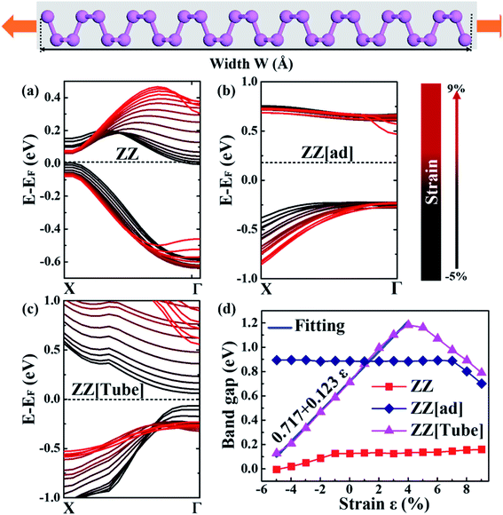
Next, we explore the strain effect on the electronic structure of PNRs before fracture. Fig. 4a–c show VBM and CBM of PNRs with different edges under variable strain/compression. For ZZ PNR, under a compressive strain from −1% to −4%, the PNR is an indirect semiconductor. When the compressive strain reaches −5%, the PNR becomes metallic with the conduction band crossing the Fermi level. Under a tensile strain (0% to 9%), the PNR is a direct semiconductor with the CBM and VBM at the X point. Both VBM and CBM drop with an increase in strain, resulting in a nearly unchanged band gap with increasing tensile stress (Fig. 4d).
For ZZ[ad] PNR, the CBM is not sensitive to strain except for a very large strain of over 7% (Fig. 4b). The VBM at the Γ point does not change much with strain even though it becomes more and more dispersive with increasing tensile stress. Therefore, the direct band gap of ZZ[ad] PNR does not change with a strain below 7%. When the strain is larger than 7%, a sudden drop in the CBM at the Γ point results in a drop in the band gap, as shown in Fig. 4d.
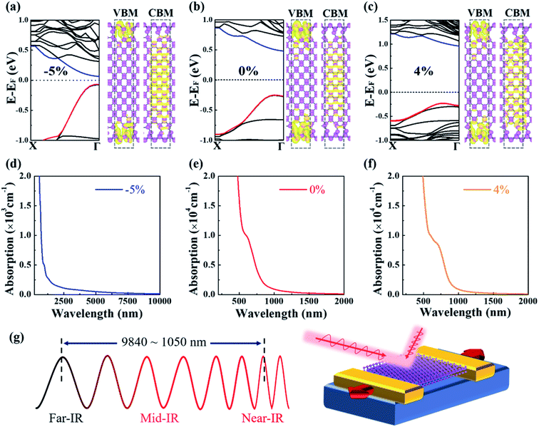
In sharp contrast with ZZ and ZZ[ad] PNRs, both CBM and VBM are very sensitive to strain for ZZ[Tube] PNR, as shown in Fig. 4c. When the strain varies from −5% to 4%, the VBM shifts downwards and the CBM shifts upwards, which results in a great increase in the band gap, from 0.13 eV to 1.18 eV (Fig. 4d). The relationship between the band gap Eg and the strain ε can be simply fitted by a linear equation as Eg = 0.717 + 0.123ε (the solid blue line in Fig. 4d). Interestingly, when the strain is over 5%, the directions of shift of the CBM and VBM are reversed and thus the band gap starts to decrease.
As shown in Fig. 1f and i, the VBM and CBM charges are spatially separated for the ZZ[Tube] PNRs with variable widths. Another question is whether the spatial charge separation is robust under strain, which is significant for applications. Plots of the charge under strains of −5%, 0% and 4% are shown in Fig. 5a–c. We can conclude that the charge separation of VBM and CBM is quite robust and can be well preserved within a strain range of −5% to 5% (Fig. S7†). In this strain range, the band gap of ZZ[Tube] PNR varies from 0.13 eV to 1.18 eV. The optical absorption spectra of ZZ[Tube] PNR under −5%, 0% and 4% strains, are shown in Fig. 5d–f, respectively. For PNR with −5%, 0% and 4% strains, the optical absorption is initially indirect adsorption and then the absorption coefficients increase sharply, implying strong direct adsorption. Such strong optical absorption ranges from 9840 nm to 1050 nm, covering the near-infrared (780–3000 nm) and mid-infrared (3000–50![[thin space (1/6-em)]](https://www.rsc.org/images/entities/char_2009.gif) 000 nm) zones (Fig. 5g), which is very physically interesting and could be technologically important. Therefore, an infrared photoelectric field effect transistor (FET) working within different spectrum ranges can be constructed using ZZ[Tube] PNRs with different widths as the conductive channel, as shown in Fig. 5g. The constructed FET can also be used as a strain sensor due to the strong dependence of the band gap on strain.
000 nm) zones (Fig. 5g), which is very physically interesting and could be technologically important. Therefore, an infrared photoelectric field effect transistor (FET) working within different spectrum ranges can be constructed using ZZ[Tube] PNRs with different widths as the conductive channel, as shown in Fig. 5g. The constructed FET can also be used as a strain sensor due to the strong dependence of the band gap on strain.
The lowest-energy and low formation barrier of tube-reconstruction,36 the robust spatial charge separation of VBM and CBM, the tunable band gap with width, linear band gap response to strain, as well as the small carrier effective mass suggest potential applications of ZZ[Tube] PNRs in optoelectronic devices based on infrared light.57–59 When the strain reaches 6% (Fig. S7†), both the CBM and VBM originate from bulk states and the charge separation disappears, which should be avoided in applications.
Conclusion
In summary, using DFT calculations, we systemically investigated the width and strain effects on the electronic properties of ZZ, ZZ[ad] and ZZ[Tube] PNRs. Due to the quantum confinement effect, the band gaps of ZZ[ad] and ZZ[Tube] PNRs increase with a decrease in the ribbon width. However, the ribbon width has little influence on the electronic properties of ZZ PNRs. Besides the ribbon width, the band gaps of ZZ[Tube] PNRs can be effectively tuned by strain in sharp contrast with ZZ and ZZ[ad] PNRs which are not sensitive to strain. ZZ[Tube] PNRs possess much smaller carrier effective masses (0.42 m0 for electrons and 1.24 m0 for holes) than ZZ[ad] PNRs and are thus more desirable for applications. Interestingly, ZZ[Tube] PNRs exhibit robust charge separation of VBM and CBM within a range of strain, from −5% to 5%. Therefore, ZZ[Tube] PNRs have the lowest energy, and ease of formation in terms of kinetics;36 they have a robust spatial charge separation of VBM and CBM; their band gap can be tuned with width; they have a linear band gap response to strain, as well as a small carrier effective mass. Therefore, ZZ[Tube] PNRs are a comprehensively promising candidate for microelectronic and optoelectric devices.Data availability
The authors indicate that the generated and analyzed data that support the findings of this study are available within the paper and ESI.†Author contributions
J. Gao, Y. Su proposed this project. M. Xia carried out all the DFT calculations. S. Li, H. Liu, L. Wang, J. Gao and J. Zhao conducted result analysis. All authors wrote and revised this manuscript.Conflicts of interest
The authors declare no competing financial or non-financial interests.Acknowledgements
This work was supported by the National Natural Science Foundation of China (Grant No. 12074053, 91961204, 12004064), by XingLiaoYingCai Project of Liaoning province, China (XLYC1907163) and by the start-up funding (DUT20RC(3)026). First-principle calculations were performed on Tianjin Supercomputing Platform and Shanghai Supercomputing Platform and the Supercomputing Center of Dalian University of Technology.References
- J. Qiao, X. Kong, Z. X. Hu, F. Yang and W. Ji, Nat. Commun., 2014, 5, 4475 Search PubMed.
- S. Lee, F. Yang, J. Suh, S. Yang, Y. Lee, G. Li, H. Sung Choe, A. Suslu, Y. Chen, C. Ko, J. Park, K. Liu, J. Li, K. Hippalgaonkar, J. J. Urban, S. Tongay and J. Wu, Nat. Commun., 2015, 6, 8573 Search PubMed.
- L. Li, Y. Yu, G. J. Ye, Q. Ge, X. Ou, H. Wu, D. Feng, X. H. Chen and Y. Zhang, Nat. Nanotechnol., 2014, 9, 372–377 Search PubMed.
- W. Li, Y. Yang, G. Zhang and Y. W. Zhang, Nano Lett., 2015, 15, 1691–1697 Search PubMed.
- F. Xia, H. Wang and Y. Jia, Nat. Commun., 2014, 5, 4458 Search PubMed.
- S. Das, W. Zhang, M. Demarteau, A. Hoffmann, M. Dubey and A. Roelofs, Nano Lett., 2014, 14, 5733–5739 Search PubMed.
- L. Li, J. Kim, C. Jin, G. J. Ye, D. Y. Qiu, F. H. da Jornada, Z. Shi, L. Chen, Z. Zhang, F. Yang, K. Watanabe, T. Taniguchi, W. Ren, S. G. Louie, X. H. Chen, Y. Zhang and F. Wang, Nat. Nanotechnol., 2017, 12, 21–25 Search PubMed.
- S. Lei, H. Wang, L. Huang, Y.-Y. Sun and S. Zhang, Nano Lett., 2016, 16, 1317–1322 Search PubMed.
- S. Susarla, A. Kutana, J. A. Hachtel, V. Kochat, A. Apte, R. Vajtai, J. C. Idrobo, B. I. Yakobson, C. S. Tiwary and P. M. Ajayan, Adv. Mater., 2017, 29, 1702457 Search PubMed.
- S. V. Morozov, K. S. Novoselov, M. I. Katsnelson, F. Schedin, D. C. Elias, J. A. Jaszczak and A. K. Geim, Phys. Rev. Lett., 2008, 100, 016602 Search PubMed.
- S. Wang, P. K. Ang, Z. Wang, A. L. Tang, J. T. Thong and K. P. Loh, Nano Lett., 2010, 10, 92–98 Search PubMed.
- C. Yan, C. Gong, P. Wangyang, J. Chu, K. Hu, C. Li, X. Wang, X. Du, T. Zhai, Y. Li and J. Xiong, Adv. Funct. Mater., 2018, 28, 1803305 Search PubMed.
- Y. Cai, Q. Ke, G. Zhang, Y. P. Feng, V. B. Shenoy and Y.-W. Zhang, Adv. Funct. Mater., 2015, 25, 2230–2236 Search PubMed.
- S. Yoon, T. Kim, S.-Y. Seo, S.-H. Shin, S.-B. Song, B. J. Kim, K. Watanabe, T. Taniguchi, G.-H. Lee, M.-H. Jo, D. Y. Qiu and J. Kim, Phys. Rev. B: Condens. Matter Mater. Phys., 2021, 103, L041407 Search PubMed.
- J. Guan, Z. Zhu and D. Tomanek, Phys. Rev. Lett., 2014, 113, 046804 Search PubMed.
- R. Fei and L. Yang, Nano Lett., 2014, 14, 2884–2889 Search PubMed.
- X. Wang, A. M. Jones, K. L. Seyler, V. Tran, Y. Jia, H. Zhao, H. Wang, L. Yang, X. Xu and F. Xia, Nat. Nanotechnol., 2015, 10, 517–521 Search PubMed.
- S. Deng, A. V. Sumant and V. Berry, Nano Today, 2018, 22, 14–35 Search PubMed.
- L. Zhu, G. Zhang and B. Li, Phys. Rev. B: Condens. Matter Mater. Phys., 2014, 90, 214302 Search PubMed.
- K. Chen, J. Deng, X. Ding, J. Sun, S. Yang and J. Z. Liu, J. Am. Chem. Soc., 2018, 140, 16206–16212 Search PubMed.
- F. Cheng, H. Xu, W. Xu, P. Zhou, J. Martin and K. P. Loh, Nano Lett., 2017, 17, 1116–1120 Search PubMed.
- L. Liu, Z. Ge, C. Yan, A. D. Moghadam, M. Weinert and L. Li, Phys. Rev. B: Condens. Matter Mater. Phys., 2018, 98, 235304 Search PubMed.
- S. Wang, L. Talirz, C. A. Pignedoli, X. Feng, K. Mullen, R. Fasel and P. Ruffieux, Nat. Commun., 2016, 7, 11507 Search PubMed.
- B. Ostahie and A. Aldea, Phys. Rev. B: Condens. Matter Mater. Phys., 2016, 93, 075408 Search PubMed.
- Y. Ren, X. Zhou and G. Zhou, Phys. Rev. B: Condens. Matter Mater. Phys., 2021, 103, 045405 Search PubMed.
- W. Hu, L. Lin, C. Yang, J. Dai and J. Yang, Nano Lett., 2016, 16, 1675–1682 Search PubMed.
- X. Zhang, J. Xin and F. Ding, Nanoscale, 2013, 5, 2556–2569 Search PubMed.
- Q. Deng and J. Zhao, Nano Lett., 2016, 16, 1244–1249 Search PubMed.
- K. Kim, S. Coh, C. Kisielowski, M. F. Crommie, S. G. Louie, M. L. Cohen and A. Zettl, Nat. Commun., 2013, 4, 2723 Search PubMed.
- Z. Liu, Y. C. Lin, C. C. Lu, C. H. Yeh, P. W. Chiu, S. Iijima and K. Suenaga, Nat. Commun., 2014, 5, 4055 Search PubMed.
- P. Koskinen, S. Malola and H. Hakkinen, Phys. Rev. Lett., 2008, 101, 115502 Search PubMed.
- P. Cui, J. H. Choi, W. Chen, J. Zeng, C. K. Shih, Z. Li and Z. Zhang, Nano Lett., 2017, 17, 1097–1101 Search PubMed.
- W. Li, G. Zhang and Y.-W. Zhang, J. Phys. Chem. C, 2014, 118, 22368–22372 Search PubMed.
- H. Guo, N. Lu, J. Dai, X. Wu and X. C. Zeng, J. Phys. Chem. C, 2014, 118, 14051–14059 Search PubMed.
- L. Liang, J. Wang, W. Lin, B. G. Sumpter, V. Meunier and M. Pan, Nano Lett., 2014, 14, 6400–6406 Search PubMed.
- J. Gao, X. Liu, G. Zhang and Y. W. Zhang, Nanoscale, 2016, 8, 17940–17946 Search PubMed.
- V. V. Ivanovskaya, A. Zobelli, P. Wagner, M. I. Heggie, P. R. Briddon, M. J. Rayson and C. P. Ewels, Phys. Rev. Lett., 2011, 107, 065502 Search PubMed.
- X. Liu, J. Gao, G. Zhang and Y.-W. Zhang, Adv. Funct. Mater., 2017, 27, 1702776 Search PubMed.
- A. Maity, A. Singh, P. Sen, A. Kibey, A. Kshirsagar and D. G. Kanhere, Phys. Rev. B, 2016, 94, 075422 Search PubMed.
- Q. Wu, L. Shen, M. Yang, Y. Cai, Z. Huang and Y. P. Feng, Phys. Rev. B: Condens. Matter Mater. Phys., 2015, 92, 035436 Search PubMed.
- X. Han, H. M. Stewart, S. A. Shevlin, C. R. Catlow and Z. X. Guo, Nano Lett., 2014, 14, 4607–4614 Search PubMed.
- T. Hu, H. Wu, H. Zeng, K. Deng and E. Kan, Nano Lett., 2016, 16, 8015–8020 Search PubMed.
- B. Huang, M. Liu, N. Su, J. Wu, W. Duan, B. L. Gu and F. Liu, Phys. Rev. Lett., 2009, 102, 166404 Search PubMed.
- Z. Z. Y. Li, S. Zhang and Z. Chen, J. Am. Chem. Soc., 2008, 130, 16739–16744 Search PubMed.
- C.-H. Park and S. G. Louie, Nano Lett., 2008, 8, 2200–2203 Search PubMed.
- Y. W. Son, M. L. Cohen and S. G. Louie, Phys. Rev. Lett., 2006, 97, 216803 Search PubMed.
- V. Sorkin and Y. W. Zhang, Nanotechnology, 2015, 26, 235707 Search PubMed.
- H. Pan and Y.-W. Zhang, J. Phys. Chem. C, 2012, 116, 11752–11757 Search PubMed.
- J. Qi, X. Qian, L. Qi, J. Feng, D. Shi and J. Li, Nano Lett., 2012, 12, 1224–1228 Search PubMed.
- P. E. Blochl, Phys. Rev. B: Condens. Matter Mater. Phys., 1994, 50, 17953–17979 Search PubMed.
- G. K. a. J. Furthmüller, Phys. Rev. B: Condens. Matter Mater. Phys., 1996, 54, 11169 Search PubMed.
- A. Cupo and V. Meunier, J. Phys.: Condens. Matter, 2017, 29, 283001 Search PubMed.
- S. I. Allec and B. M. Wong, J. Phys. Chem. Lett., 2016, 7, 4340–4345 Search PubMed.
- Y. Cai, G. Zhang and Y. W. Zhang, Sci. Rep., 2014, 4, 6677 Search PubMed.
- V. Tran, R. Soklaski, Y. Liang and L. Yang, Phys. Rev. B: Condens. Matter Mater. Phys., 2014, 89, 235319 Search PubMed.
- M. Wu and X. C. Zeng, Nano Lett., 2016, 16, 3236–3241 Search PubMed.
- X. Ling, H. Wang, S. Huang, F. Xia and M. S. Dresselhaus, Proc. Natl. Acad. Sci. U. S. A., 2015, 112, 4523–4530 Search PubMed.
- N. Youngblood, C. Chen, S. J. Koester and M. Li, Nat. Photonics, 2015, 9, 247–252 Search PubMed.
- A. S. Rodin, A. Carvalho and A. H. Castro Neto, Phys. Rev. Lett., 2014, 112, 176801 Search PubMed.
Footnote |
| † Electronic supplementary information (ESI) available. See DOI: 10.1039/d1na00332a |
| This journal is © The Royal Society of Chemistry 2021 |

