 Open Access Article
On-surface chemistry using local high electric fields†
Thomas
Leoni
,
Tony
Lelaidier
,
Anthony
Thomas
,
Alain
Ranguis
,
Olivier
Siri
 ,
Claudio
Attaccalite
and
Conrad
Becker
 *
*
Aix Marseille University, CNRS, CINaM UMR 7325, Campus de Luminy, 13288 Marseille Cedex 09, France. E-mail: conrad.becker@univ-amu.fr
First published on 7th August 2021
Abstract
Dihydrotetraazapentacene (DHTAP) molecules can be dehydrogenated on the surface to form tetraazapentacene (TAP), by applying a high electric field between the tip of a scanning tunnelling microscope (STM) and a metallic substrate in the zero-current limit. The method can be applied either to single molecules or more extended layers by successively scanning a selected area using an STM tip.
On-surface chemistry is a promising topic in nanoscience and is widely applied for the generation of a multitude of nanostructures and to the local chemical modification of adsorbed molecules in order to tune their properties or create layers with new functionalities. As examples for the first, we can cite on-surface synthesis by reactive coupling of adsorbed molecules.1,2 The second mechanism concerns the direct chemical modification of adsorbed species at the molecular level by inelastic electron tunnelling from a scanning tunnelling microscope (STM) tip.3 Both approaches have their virtues being either very efficient and atomically precise on the nanoscale for the former or being highly local down to the single molecule (bond) level for the latter. Our approach is a variant of the latter scheme which is based on the application of a high electric field between the tip of an STM and a metallic substrate across a well-organized double layer of organic molecules.
Using an electric field to control chemical reactions is a concept that has been discussed in the early works of Shaik et al.4 and for example successfully applied to the electrostatic catalysis of a Diels–Alder reaction.5 In fact, electrochemistry is based on the modification of the chemical potential by applying a voltage between the two electrodes of an electrochemical cell in order to initiate redox reactions. This implies, however, a charge transport using an electrolyte and this scheme is not applicable ultra-high vacuum. Here we address the following question: can a dehydrogenation reaction in vacuum be triggered by an electric field gradient in the absence of electron tunnelling and thus in the zero-current limit? This mechanism has been successfully demonstrated for some rare cases such as the isomerization of azobenzene,6 the cleavage of a carbon–sulphur bond in thiophene on Cu(111)7 and ring-closing reactions on single diarylethene derivatives on Ag(111).8 We use a similar approach that extends the field-induced chemical modification of single molecules by STM to the modification of extended layers. As a prototype molecule, we here use dihydrotetraazapentacene (DHTAP, see Scheme 1), which belongs to a class of azapentacene precursors that have been widely discussed in literature as candidates for applications as organic semiconductors due to their superior environmental stability as compared to pentacene.9,10 Unfortunately, these molecules possess bigger bandgaps than their acene analogues and the charge carrier mobility in azaacene films is relatively low. The latter problem can in the case of DHTAP be circumvented by the growth of highly organized films,11 but the former problem is intrinsic to the rupture of the π-electron delocalization by the presence of NH groups.12 A possible solution to this problem would thus be to dehydrogenate the NH groups, which would yield the fully conjugated tetraazapentacene (TAP) (see Scheme 1), a molecule which has so far not been synthesized by conventional organic chemistry.
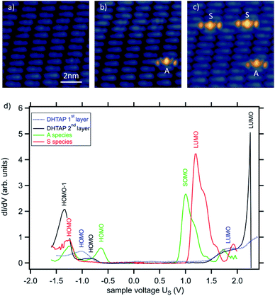
Here we have chosen a double layer of DHTAP on Au(111) that was previously reported to be very well organized due to hydrogen bonding between adjacent DHTAP molecules in the first layer, which stabilizes the morphology.11 The layers have been prepared by thermal evaporation of DHTAP in ultra-high vacuum (UHV) onto an Au(111) single crystal surface kept at 250 K. The STM experiments were performed at a temperature of 78 K using electrochemically etched W-tips. The bias voltage values correspond to the sample potential. Using this approach, we produced highly ordered layers with extended second layer islands in the coverage range from 1.2 to 1.5 ML. These islands are always compact, and no individual molecules could be observed due to the relatively high sample temperature during deposition for which the mobility of the DHTAP is very high (see ESI†). While scanning these double layers at different positive sample voltages Us it can be observed that a few second layer molecules show an enhanced brightness above a certain threshold voltage (see Fig. 1). According to their characteristic shapes, we denote the species that appears above Us = 1.05 V as asymmetric (A) and the species that appears above Us = 1.3 V as symmetric (S). This phenomenon may either arise from a different coupling of the molecules to the substrate that could modify electron tunnelling or are chemical modification of the respective molecules. In the following we will show that the latter is at the origin of the enhanced molecular contrast and that the STM tip can be used to locally induce the chemical modification of the DHTAP.
The successive appearance of A and S species as a function of the sample voltage can easily be understood by looking at scanning tunnelling spectra (STS) in Fig. 1d, which have been acquired on top of the different species. These spectra clearly show that the LUMO of the second layer DHTAP is located above 2.2 V whereas the correspond orbitals of the A species and the S species are located at 1.0 V and 1.2 V, respectively. The small increase of the dI/dV signal observed around 1.8 V can be attributed to a contribution of the LUMO of the DHTAP molecules of the first monolayer, for which the STS spectrum is shown as a reference. The spectra corroborate our assumption that the enhanced contrast of the A and S in the STM images stems from the imaging of the frontier orbitals of the respective species and is perfectly in line with the observed threshold voltages. We can exclude that the observed shifts of the molecular orbitals are due to negative charging of the DHTAP by the tunnelling electrons since the energy of the LUMO of the DHTAP should be displaced to higher energies in this case. We conclude, thus, that the type A, S and DHTAP molecules are three distinct chemical species.
To unequivocally identify the observed species, we have undertaken DFT calculations of isolated molecules of the different molecular species using GAMESS and Quantum Espresso13 (see ESI† for details). Two of the investigated species are in good agreement with features of the A and S species observed by STM. The calculated LUMO of tetraazapentacene (TAP) and the SOMO (singly occupied molecular orbital) of monohydrotetraazapentacene (MHTAP) are compared with the molecular orbitals observed by STM in Fig. 2. We have omitted the DHTAP LUMO in this figure since molecular shape of the LUMO cannot be easily detected for this species (see the series of STM images at different sample voltages and the calculated DHTAP LUMO in the ESI†). The chemical structure of TAP molecules possesses two axes of symmetry, along the short and the long molecular axis, respectively. This symmetry is also reflected in the STM image and the calculated LUMO. The MHTAP chemical structure possesses no symmetry axis due to the missing hydrogen. In the corresponding STM image, we can observe a W-shaped structure that can easily be attributed to the NH and N˙ groups, respectively, by comparing the STM image with the calculated SOMO. It should be noted that in the calculation the shape is rather butterfly-like, which could indicate that the molecule on the surface is slightly rotated along the long molecular axis. The energies of the gap of the different species can be found in Table 1. The correspondence between the theoretical value and the experimental values is quite good.
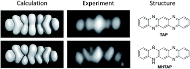 | ||
| Fig. 2 Comparison of the calculated frontier orbitals (LUMO for TAP and SOMO for MHTAP) tilted by a 30° angle about the long molecular axis and molecular orbitals observed by STM. The LUMO of DHTAP is not shown because the molecules are not easily identifiable in the corresponding sample voltage range (see ESI†). | ||
| Molecular species | Calculated [eV] | Experiment [eV] |
|---|---|---|
| DHTAP | 2.95 | ≥3.11 |
| TAP | 2.34 | 2.46 |
| MHTAP | 1.77 | 1.63 |
The presence of the three different molecules is quite intriguing and suggests that DHTAP can undergo a transformation to either MHTAP or TAP during or after deposition. The presence of either molecule in the DHTAP powder that was used for evaporation has been excluded by NMR spectroscopy analysis.
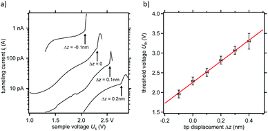
We have thus turned to a systematic study of the chemical modification of DHTAP molecules in the second layer using an electric field applied between the substrate and the STM tip. Our initial approach was to use inelastic electron tunnelling, which in the past had successfully been applied for the dehydrogenation of adsorbed molecules such as ethene,14 benzene,15 propene16 and H2TPP.17 This approach was in fact successful in the first and the second layer for small tip–sample distances but in the first layer only TAP was obtained (see ESI†). By extending these experiments to different tip–sample distances, we noticed that in the series of experiments shown in Fig. 3 the threshold voltage for the dehydrogenation of the DHTAP is a function of the tip–sample distance. The dehydrogenation events in Fig. 3a are identified by arrows and can be attributed to the sudden increase of the tunnelling current. For these experiments the tip was stabilized above a DHTAP molecule at sample voltage of Us = 1.3 V and a tunnelling current of It = 20 pA and the feedback loop was stopped to stabilize the tip sample distance z. The tip was then retracted from the surface by a distance Δz and an I–V scan was launched during which the tunnelling current was recorded. Subsequently, STM images were recorded to verify that a dehydrogenation event had taken place. The series of experiments conducted results in the curve shown in Fig. 3b, which represents the dependence of the threshold voltage Uth, corresponding to the sudden increase of the tunnelling current in Fig. 3a, on the relative tip–sample distance Δz. It should be noted that for displacements of Δz > 0.4 nm the tunnelling current at Uth was below the noise level (It ≈ 300 fA) of the preamplifier used so that we were not able determine the threshold electric field by this method. The least squares fit of the data points in Fig. 3b yields the value of the electric field E = (2.67 ± 0.07) V nm−1 that is needed to trigger a dehydrogenation event.
Even though a measurement of the dehydrogenation threshold was not possible at higher Δz for the reasons mentioned above we could, however, observe dehydrogenation events (see Fig. 4). In this case, for Δz = 0.9 nm, the voltage ramp was replaced by a voltage pulse of 1 s duration. It can clearly be seen that by applying successive pulses on the same molecule we can produce first MHTAP and then TAP from a single DHTAP molecule. One should note that under these conditions the tunnelling current is extremely low and can be estimated to equal It ≈ 200 zA, which corresponds to roughly one electron per second (see ESI†). We can, thus, clearly exclude that inelastic tunnelling is at the origin of the observed dehydrogenation events at large tip sample distances since inelastic tunnelling usually concerns less than 1% of all tunnelling electrons.2 It may, however, contribute to the dehydrogenation of DHTAP at small tip–sample distances but we have not obtained conclusive data on the relative importance of the two mechanisms in this case and we have chosen to focus here on the novel field-induced dehydrogenation.
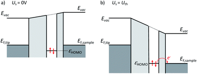
If the dehydrogenation is caused by the applied field, it must be related to energetic positions of the molecular orbitals of the second layer DHTAP. This situation is schematically depicted in Fig. 5, where the HOMO (highest occupied molecular orbital) of the second layer DHTAP is placed at εHOMO = 0.82 eV below the Fermi energy EF,sample of the Au(111) substrate, an energy that was experimentally determined by STS (see ESI†). It is well known that a molecular monolayer can act as a buffer layer to provide an electronic decoupling of subsequent layers.18 It should be noted that the second DHTAP layer is physisorbed and thus electronically decoupled from the substrate. This means that the energetic position of the HOMO is determined by the ionization potential of the molecule referred to the vacuum energy Evac in the gap much like for physisorbed rare gas atoms on metal surfaces.19 If we now apply a positive voltage to the sample, the HOMO of the second layer DHTAP will be displaced relative to the Fermi energy of the sample EF,sample due to the modification of Evac in the gap and eventually align with it. Starting at this voltage electrons from the DHTAP HOMO can tunnel through the monolayer, which represents in this case a tunnelling barrier, into the metal bulk creating either a singly or doubly charged DHTAP cation. In a second step, the corresponding cation can restore its neutrality by deprotonation20 of the NH-group (see ESI†), which will lead to either MHTAP or TAP depending on the initial charge state. The proposed mechanism is inspired the one proposed by Fernandez-Torrente et al. for the changing of the charge state of single molecules by STM.21 The fact that MHTAP has been identified as a product implies that the dehydrogenated molecules belong to the second layer since MHTAP, being a radical, would not be stable in the first layer in contact with the metallic substrate. This again stresses the importance of the first layer that electronically decouples the molecules in the second layer from the substrate.
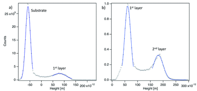
In the framework of this model, the threshold voltage Uth should depend on Δz in a linear manner as observed experimentally if we assume that the tip–sample electrode system can be treated as a planar capacitor. In this case the electric field necessary to align the onset of HOMO (εonset = −(0.7 ± 0.2) eV) of the DHTAP (see ESI†) with the Fermi energy of the sample can be derived from E = |Uth|/h, where h is the height of the second DHTAP layer above the metal surface. To estimate the height of the second layer above the metal substrate we have measured the relative height of the DHTAP layers using the histograms shown in Fig. 6. The mean heights of the substrate, the first and the second layer have been evaluated using Gaussian fits of the histograms. For the first DHTAP layer this yields a value of h1 = (120 ± 10) pm and for the second layer a value of h2 = (147 ± 10) pm has been found. We thus conclude that the height of the second layer molecules above the metal substrate corresponds to h = h1 + h2 = (267 ± 20) pm.
Using this value and the value of the threshold voltage Uth = −(0.7 ± 0.2) V the calculation yields a value for E = (2.62 ± 0.36) V nm−1 that corresponds well to the value derived from the least squares fit in Fig. 3b, which was E = (2.67 ± 0.07) V nm−1. This corroborates our interpretation of an electric field induced dehydrogenation of DHTAP. It should be noted that the dehydrogenation has only been observed for positive sample voltages since negative sample voltages would, according to the model in Fig. 5, result in a shift of the DHTAP HOMO in the opposite direction.
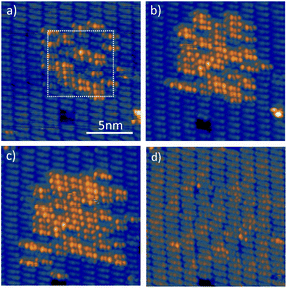
As we have shown above, this method works perfectly well for single molecules in a dense molecular layer, but we occasionally observed that adjacent molecules were also dehydrogenated. We have thus extended our experiments to the dehydrogenation of larger areas. To this end, we scanned with the tip of the STM over the DHTAP bilayer at constant height and constant voltage with the feedback loop turned off (see Fig. 7). As in the case of the single molecule dehydrogenation the tip was retracted by Δz = 1 nm from the initial tunnelling setpoint (It = 20 pA, Us = 1.3 V), which ensured zero-current conditions, and a sample voltage of 4.2 V was applied during the scan. After the first scan the molecules which have undergone dehydrogenation are visible in Fig. 7a. After a second scan of the same area, the number of dehydrogenated DHTAP molecules has significantly increased (Fig. 7b). A third scan was carried out on slightly increased area of 10 nm × 10 nm and again the number of dehydrogenated molecules is increased (Fig. 7c). In the final state, we have identified 19 MHTAP and 47 TAP molecules, which means that ≈45% of the scanned area is covered with TAP and 19% with MHTAP so that roughly two thirds of the DHTAP molecules have been dehydrogenated by this method. One should note that structure of the molecular layer is virtually unperturbed by the successive dehydrogenation as can be seen in Fig. 7d which was acquired at a negative sample voltage for which STM shows little difference between the molecular species. This may be surprising given that after dehydrogenation of the layer via H-bonding is no longer possible. We assume, however, that the van der Waal bonding between the second layer molecules and the first layer molecules is still sufficient to conserve the structural integrity of the second layer at the investigated temperature (78 K). Finally, we conclude that a well-ordered layer of TAP could be produced from an electronically decoupled DHTAP layer using high electric fields.
Conclusions
We reported on the dehydrogenation of DHTAP molecules by locally applying a high electric field. Using this method, we could demonstrate the on-surface synthesis of TAP and MHTAP from DHTAP in a self-assembled layer by the double or single dehydrogenation, respectively. The dehydrogenation is induced by the electric field between the STM tip and the sample of the order of E = 2.67 V nm−1 that will shift the HOMO of the second layer DHTAP molecules from its initial position εHOMO = −0.82 eV above the Fermi energy of the metallic substrate. This results in a dehydrogenation mechanism of DHTAP, which is mediated by the creation of transient cations that stabilize by deprotonation. We have shown that it is possible to dehydrogenate either individual molecules by voltage pulses or a group of molecules by scanning a larger area at high voltages. Our observations suggest that it could be possible to prepare large-scale TAP layers via the non-local application of a high electric field to electronically decoupled DHTAP layers.Conflicts of interest
There are no conflicts to declare.Acknowledgements
The authors acknowledge the financial support of the project by the French Agence Nationale de la Recherche (ANR) through Grant ANR 14 CE34 0003 01.Notes and references
- X. Zhang, Q. Zeng and C. Wang, Nanoscale, 2013, 5, 8269 RSC.
- Q. Shen, H.-Y. Gao and H. Fuchs, Nano Today, 2017, 13, 77–96 CrossRef CAS.
- T. Komeda, Prog. Surf. Sci., 2005, 78, 41–85 CrossRef CAS.
- S. Shaik, S. de Visser and D. Kumar, J. Am. Chem. Soc., 2004, 126, 11746 CrossRef CAS.
- A. C. Aragonès, N. L. Haworth, N. Darwish, S. Ciampi, N. J. Bloomfield, G. G. Wallace, I. Diez-Perez and M. L. Coote, Nature, 2016, 531, 88–91 CrossRef PubMed.
- M. Alemani, M. V. Peters, S. Hecht, K. Rieder, F. Moresco and L. Grill, J. Am. Chem. Soc., 2006, 128, 14446–14447 CrossRef CAS PubMed.
- B. Borca, T. Michnowicz, R. Pétuya, M. Pristl, V. Schendel, I. Pentegov, U. Kraft, H. Klauk, P. Wahl, R. Gutzler, A. Arnau, U. Schlickum and K. Kern, ACS Nano, 2017, 11, 4703–4709 CrossRef CAS PubMed.
- G. Reecht, C. Lotze, D. Sysoiev, T. Huhn and K. J. Franke, J. Phys.: Condens. Matter, 2017, 29, 294001 CrossRef PubMed.
- U. H. F. Bunz, J. U. Engelhart, B. D. Lindner and M. Schaffroth, Angew. Chem., Int. Ed., 2013, 52, 3810–3821 CrossRef CAS PubMed.
- C. Di, J. Li, G. Yu, Y. Xiao, Y. Guo, Y. Liu, X. Qian and D. Zhu, Org. Lett., 2008, 10, 3025–3028 CrossRef CAS PubMed.
- T. Lelaidier, T. Leoni, P. Arumugam, A. Ranguis, C. Becker and O. Siri, Langmuir, 2014, 30, 5700–5704 CrossRef CAS PubMed.
- J. I. Wu, C. S. Wannere, Y. Mo, P. V. R. Schleyer and U. H. F. Bunz, J. Org. Chem., 2009, 74, 4343–4349 CrossRef CAS PubMed.
- M. S. Gordon, J. H. Jensen, S. Koseki, N. Matsunaga, K. A. Nguyen, S. Su, T. L. Windus, M. Dupuis and J. A. Montgomery, J. Comput. Chem., 1993, 14, 1347–1363 CrossRef; P. Giannozzi, S. Baroni, N. Bonini, M. Calandra and R. Car, et al. , J. Phys.: Condens. Matter, 2009, 21, 395502 CrossRef PubMed.
- J. Gaudioso, H. J. Lee and W. Ho, J. Am. Chem. Soc., 1999, 121, 8479–8485 CrossRef CAS.
- M.-L. Bocquet, H. Lesnard and N. Lorente, Phys. Rev. Lett., 2006, 96, 96101 CrossRef PubMed.
- M. Parschau, K. H. Rieder, H. J. Hug and K.-H. Ernst, J. Am. Chem. Soc., 2011, 133, 5689–5691 CrossRef CAS PubMed.
- V. D. Pham, V. Repain, C. Chacon, A. Bellec, Y. Girard, S. Rousset, A. Smogunov, Y. J. Dappe and J. Lagoute, J. Phys. Chem. Lett., 2016, 7, 1416–1421 CrossRef CAS PubMed.
- M. Feng, L. Gao, S. X. Du, Z. T. Deng, Z. H. Cheng, W. Ji, D. Q. Zhang, X. F. Guo, X. Lin and L. F. Chi, et al. , Adv. Funct. Mater., 2007, 17, 770–776 CrossRef CAS.
- K. Wandelt, Appl. Surf. Sci., 1997, 111, 1–10 CrossRef CAS.
- L. Sawtschenko, K. Jobst, A. Neudeck and L. Dunsch, Electrochim. Acta, 1996, 41, 123–131 CrossRef CAS.
- I. Fernandez-Torrente, D. Kreikemeyer-Lorenzo, A. Strozecka, K. J. Franke and J. I. Pascual, Phys. Rev. Lett., 2012, 108, 036801 CrossRef CAS PubMed.
Footnote |
| † Electronic supplementary information (ESI) available. See DOI: 10.1039/d1na00383f |
| This journal is © The Royal Society of Chemistry 2021 |


