
 Open Access Article
 This Open Access Article is licensed under a Creative Commons Attribution-Non Commercial 3.0 Unported Licence
Rectifying optoelectronic memory based on WSe2/graphene heterostructures†
Sung Hyun
Kim
a,
Myung Uk
Park
a,
ChangJun
Lee
a,
Sum-Gyun
Yi
a,
Myeongjin
Kim
a,
Yongsuk
Choi
b,
Jeong Ho
Cho
 b and
Kyung-Hwa
Yoo
*a
b and
Kyung-Hwa
Yoo
*a
aDepartment of Physics, Yonsei University, 50 Yonsei-ro, Seoul, 03722, Republic of Korea. E-mail: khyoo@yonsei.ac.kr
bDepartment of Chemical and Biomolecular Engineering, Yonsei University, 50 Yonsei-ro, Seoul, 03722, Republic of Korea
First published on 20th July 2021
Abstract
van der Waals heterostructures composed of two-dimensional materials vertically stacked have been extensively studied to develop various multifunctional devices. Here, we report WSe2/graphene heterostructure devices with a top floating gate that can serve as multifunctional devices. They exhibit gate-controlled rectification inversion, rectified nonvolatile memory effects, and multilevel optoelectronic memory effects. Depending on the polarity of the gate voltage pulses (VGp), electrons or holes can be trapped in the floating gate, resulting in rectified nonvolatile memory properties. Furthermore, upon repeated illumination with laser pulses, positive or negative staircase photoconductivity is observed depending on the history of VGp, which is ascribed to the tunneling of electrons or holes between the WSe2 channel and the floating gate. These multifunctional devices can be used to emulate excitatory and inhibitory synapses that have different neurotransmitters. Various synaptic functions, such as potentiation/depression curves and spike-timing-dependent plasticity, have been also implemented using these devices. In particular, 128 optoelectronic memory states with nonlinearity less than 1 can be achieved by controlling applied laser pulses and VGp, suggesting that the WSe2/graphene heterostructure devices with a top floating gate can be applied to optoelectronic synapse devices.
Introduction
van der Waals (vdW) materials, such as graphene, semiconducting transition metal dichalcogenides, and hexagonal boron nitride (hBN), have received considerable attention owing to their possible applications in ultrathin, flexible, and transparent electronic and optoelectronic devices.1–4 In particular, vdW heterostructures, in which different vdW materials are vertically stacked, have been extensively studied to develop multifunctional devices.5–7 For example, various hybrid heterostructures, such as PtS2/h-BN/graphene,8 graphene/hBN/MoS2,y![[thin space (1/6-em)]](https://www.rsc.org/images/entities/char_2009.gif) 9 MoS2/hBN/graphene or MoS2,10 and graphene/hBN/ReSe211 exhibit multibit optoelectronic nonvolatile memory effects. When these heterostructures are irradiated with laser pulses, the conductance increases in a staircase behavior, enabling multilevel optical erasing, whereas multilevel programming is achieved by applying gate voltage pulses (VGp). In contrast to traditional random-access memories (RAMs), optoelectronic random-access memories (ORAMs) can store light information with an electronic readout at low programming voltages. Processing with light as an extra control parameter provides features such as optical and arithmetic logic operations and the simultaneous detection of electrical and optical signals. Furthermore, image-capturing circuits are simplified by the integration of optical sensors and memory devices in ORAMs.
9 MoS2/hBN/graphene or MoS2,10 and graphene/hBN/ReSe211 exhibit multibit optoelectronic nonvolatile memory effects. When these heterostructures are irradiated with laser pulses, the conductance increases in a staircase behavior, enabling multilevel optical erasing, whereas multilevel programming is achieved by applying gate voltage pulses (VGp). In contrast to traditional random-access memories (RAMs), optoelectronic random-access memories (ORAMs) can store light information with an electronic readout at low programming voltages. Processing with light as an extra control parameter provides features such as optical and arithmetic logic operations and the simultaneous detection of electrical and optical signals. Furthermore, image-capturing circuits are simplified by the integration of optical sensors and memory devices in ORAMs.
Herein, we report a WSe2/graphene heterostructure device with a photoresponsive top floating gate. The heterostructure without the top layer exhibited gate-tunable rectifying characteristics without memory effects, which is ascribed to the mismatch between the Fermi levels of graphene and WSe2 and the ambipolar properties of WSe2.12 However, the heterostructure with a MoS2 top layer exhibited rectifying nonvolatile memory effects with an on/off ratio of ∼104 and a retention time of >103 s, indicating that the MoS2 top layer acts as a charge trapping layer or floating gate. Kelvin probe force microscopy (KPFM) images revealed that holes and electrons were trapped in the top floating gate by applying VGp < 0 and VGp > 0, respectively, resulting in rectifying nonvolatile memory behaviors. Furthermore, our devices exhibited multilevel optoelectronic memory effects. However, unlike most of the reported optoelectronic devices,9–11 multilevel programming was achieved by repeated illumination, whereas multilevel erasing was obtained by repeated illumination with laser pulses combined with VGp.
These gate-tunable rectified multilevel optoelectronic memory properties will pave the way for various future applications. One potential application is in optoelectronic synapse devices. Recently, a variety of two-terminal memristors13–16 and three-terminal devices17–21 have been explored as artificial synapses for emulating biological synaptic functions. More recently, optoelectronic synapses based on MoOx,22 phase-change materials,23 and black phosphorous/PxOy24 have also been demonstrated. However, although there are two types of biological synapses, called excitatory and inhibitory synapses, which have different neurotransmitters,25–27 most devices emulate only excitatory synapses. If excitatory neurotransmitters bind to receptors in a postsynaptic neuron, ligand-gated ion channels open and positive ions flow into the cell, generating excitatory postsynaptic currents (EPSCs). In contrast, if inhibitory neurotransmitters bind to receptors, negative ions flow into the cell through ion channels, generating inhibitory postsynaptic currents (IPSCs). For an action potential to occur, the sum of the EPSCs and IPSCs must exceed a threshold value. The balance between excitation and inhibition is very important in the brain. If the balance is disrupted, diseases such as epilepsy can occur.28
To investigate whether rectified nonvolatile memory effects can be applied to emulate inhibitory synapses as well as excitatory synapses, two similar devices were connected in parallel. Similar to the addition of EPSCs and IPSCs, the total conductance increased or decreased depending on the polarity of VGp applied to the two devices. In addition, various synaptic functions, including potentiation and depression processes, and spike-timing-dependent plasticity (STDP) could be emulated, and the recognition rate was simulated to be approximately 72% using an artificial neural network (ANN) based on a single-layer perceptron (SLP) model. These results demonstrate that the WSe2/graphene heterostructures with a top floating gate can be applied to optoelectronic synapse devices.
Results and discussion
Electrical characteristics of a WSe2/graphene heterostructure
First, we fabricated a WSe2/graphene heterostructure on an hBN (∼11 nm)/SiO2/p++-Si substrate with prepatterned Au electrodes to avoid the high Schottky barrier,29,30 where a gate voltage (VG) was applied using the p++-Si substrate. Mechanically exfoliated few-layer graphene (∼12 nm) and WeS2 flakes (∼10 nm) were transferred onto the electrodes, resulting in a WSe2/graphene heterostructure (Fig. 1(a)). Initially, the source-drain current (ISD)–voltage (VSD) curve of this device showed negligible conductance (Fig. S1†). However, when the ISD–VG transfer curves were measured by sweeping VG from −60 to +60 V and back to −60 V, p-type and n-type semiconducting behaviors were observed at VSD = −1 and +1 V, respectively (Fig. 1(b)). Accordingly, when VG ≪ 0, ISD exhibited finite values at VSD < 0, whereas ISD was negligible at VSD > 0, leading to rectifying characteristics (Fig. 1(c)). In contrast, when VG ≫ 0, the rectification direction was inverted: ISD was finite only for VSD > 0. Similar gate-controlled rectifying behaviors have also been reported in other studies.12,31,32 | ||
| Fig. 1 (a) Schematic of a WSe2 field-effect device with graphene and Au electrodes. (b) ISD–VG transfer curves measured at VSD = −1 V (blue symbols) and +1 V (red symbols) by sweeping VG from −60 to +60 and back to −60 V. The inset shows an optical image of the device. (c) ISD–VSD curves measured when different values of VG were applied. (d) Energy band diagrams before applying VG (top), with VG ≪ 0 (middle) and VG ≫ 0 (bottom). | ||
This gate-tunable rectification inversion is explained by the energy band diagrams shown in Fig. 1(d). The bandgap (Eg) and electron affinity (χ) of the multilayer WSe2 are approximately 1.3 and 3.5 eV, respectively,33,34 and the workfunction (φ) is 4.56 and 5.1 eV for graphene and Au, respectively.34,35 If VG ≪ 0, the Fermi level shifts downward and the major charge carriers become holes. At VSD < 0, the holes can move from the graphene to WSe2, leading to finite currents. However, at VSD > 0, the holes cannot flow into the graphene because of the gate-induced Fermi level mismatch between graphene and WSe2, resulting in a rectifying behavior. In contrast, if VG ≫ 0, the Fermi level shifts upward and the major charge carriers are electrons that can flow from the WSe2 to the Au electrode only at VSD > 0. Thus, the rectification direction is inverted.
Memory properties of a WSe2/graphene heterostructure with a MoS2 floating gate
Next, we fabricated a WSe2/graphene heterostructure with a MoS2 top layer by transferring hBN (∼10 nm) and MoS2 (∼11 nm) flakes onto the heterostructure (Fig. 2(a)). The ISD–VG transfer curves, which were measured by sweeping VG from −50 to +50 V and back to −50 V, showed n-type and p-type semiconducting behaviors at VSD > 0 and VSD < 0, respectively, as in the WSe2/graphene heterostructure without the MoS2 top layer (Fig. 2(b)). However, the ISD–VG transfer curves of this device exhibited large hysteresis for both polarities of VSD, indicating that the MoS2 top layer acted as the floating gate, although the MoS2 layer was placed on the top of the heterostructure, unlike the conventional flash memory devices that have a floating gate between a channel and a control gate. To characterize the nonvolatile memory effects, VGp of −50 V or +50 V with a pulse width of 0.1 s was applied, and ISD was measured at VSD = +1 V (Fig. S2(a)†). The device was switched to the on state by applying VGp = −50 V and to the off state by applying VGp = +50 V. On the other hand, the application of VGp = −50 and +50 V induced the off and on states, respectively, at VSD = −1 V. For both cases, the on/off ratio was ∼104 and the retention time was estimated to be longer than 103 s. To further investigate the nonvolatile memory properties, ISD was measured when ±1 V square waves were applied to the VSD after applying VGp with different amplitudes (Fig. 2(c)). The rectified multilevel memory states were obtained. When triangular waves were applied to VSD after applying different VGp, similar rectified multilevel memory effects were also observed (Fig. S2(b)†).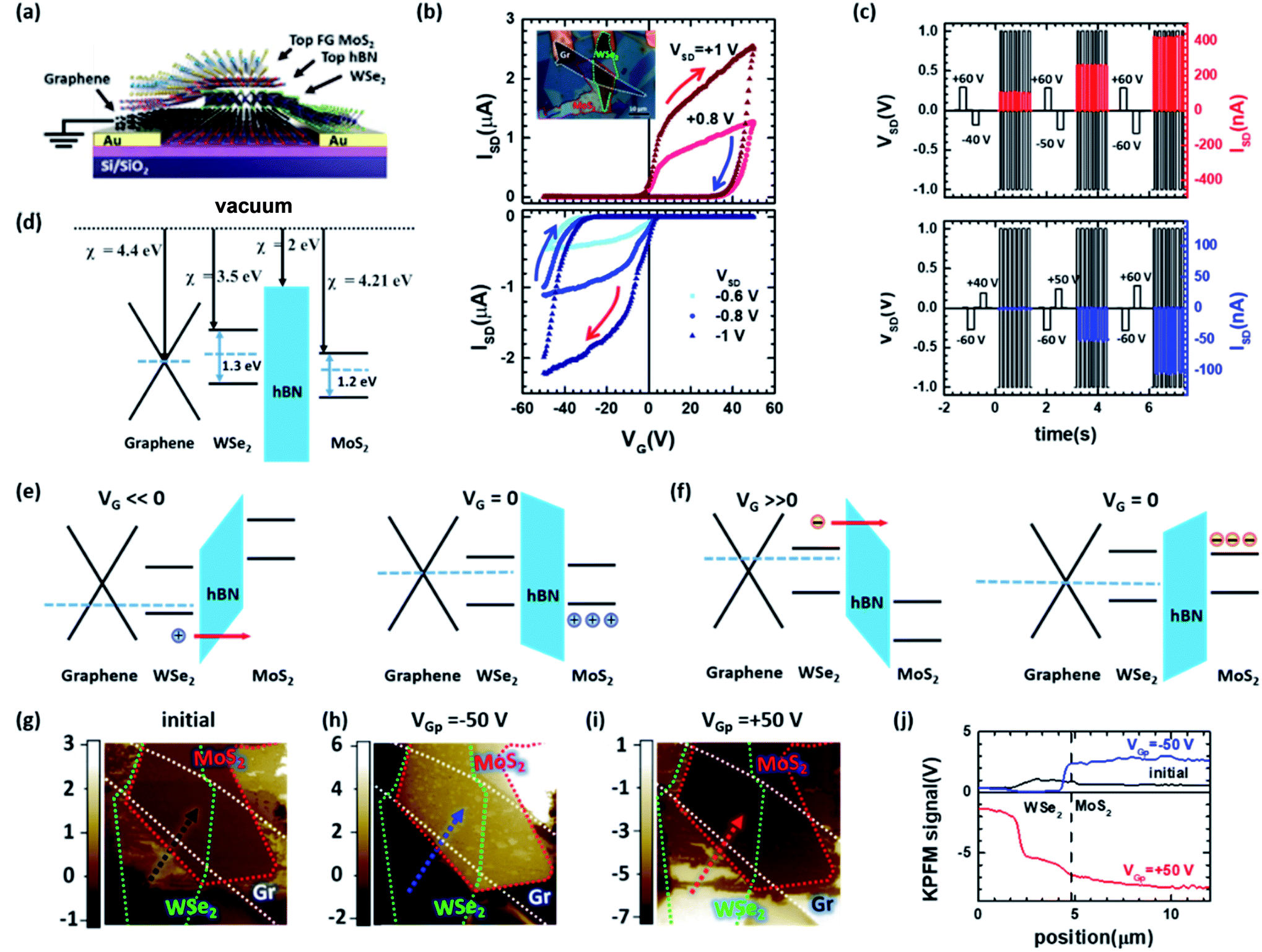 | ||
| Fig. 2 (a) Schematic of a WSe2-based device with a MoS2 top layer. (b) ISD–VG transfer curves measured at various VSD by sweeping VG from −50 to +50 V and back to −50 V. (c) ISD measured at VSD of ±1 V square waves with a frequency of 5 Hz after applying various VGp. Before each measurement, the device was reset by applying VGp = +60 (top) or VGp = −60 V (bottom). Energy band diagrams in (d) a flat band, (e) with VGp ≪ 0 and (f) VGp ≫ 0. χ represents an electron affinity. KPFM images acquired (g) before applying VG, (h) after applying VGp = −50 V and (i) VGp = +50 V. Green, white, and red dashed lines indicate WSe2, graphene, and MoS2, respectively. (j) Line profile of KPFM signals indicated by arrow lines in (g), (h), and (i). | ||
To explain the rectified nonvolatile memory effects, we propose the energy band diagrams shown in Fig. 2(d)–(f). If a negative voltage pulse with a large amplitude is applied to VG, the Fermi level shifts downward, and the tunneling barrier is lowered (Fig. 2(e)). Consequently, holes can tunnel from the WSe2 channel to the MoS2 layer through the hBN. However, when VG returns to 0 V, the tunneling barrier increases again, and the holes become trapped in the MoS2 layer. The trapped holes shift the Fermi level upward, and the device is switched to the on state at VSD > 0 and to the off state at VSD < 0, as shown in Fig. 1(d). In contrast, if a positive voltage pulse with a large amplitude is applied to VG, electrons tunnel from the WSe2 channel to the MoS2 layer via the Fowler–Nordheim tunneling mechanism, and are trapped in the MoS2 floating gate (Fig. 2(f)), which results in the on state at VSD < 0 and the off state at VSD > 0. Fig. 2(g)–(i) show KPFM images acquired before applying VGp and after applying VGp = −50 and +50 V, respectively. Positive/negative KPFM signals indicate the accumulation of positive/negative charges,36,37 and these KPFM images support that the rectified nonvolatile memory effects are attributed to the trapping of holes and electrons in the MoS2 top floating gate induced by the application of VGp = −50 and +50 V, respectively (Fig. 2(j)).
Optoelectronic performances of a WSe2/graphene heterostructure with a MoS2 floating gate
Illumination with laser pulses was reported to induce multilevel memory states in MoS2-based devices with a floating gate;9,10 hence, we also investigated whether our WSe2/graphene device with the MoS2 top layer exhibited multilevel optical memory effects. First, the device was switched to the off state at ISD = +1 V by applying VGp = +50 V, which induced electrons trapped in the MoS2 layer and led to p-type behaviors. The light pulses were then illuminated (Fig. 3(a)). ISD increased during irradiation but returned to the off state in dark, unlike most reported electronic memory devices, in which ISD increased stepwise upon repeated illumination with laser pulses. In the case of our devices, holes should be trapped in the MoS2 floating gate to obtain a stepwise increase in ISD at VSD = +1 V. These results imply that hole trapping was not induced by illumination. To make holes tunnel from WSe2 to MoS2, VGp ≪ 0 is required (Fig. 2(e)). When VGp = −25 or −32 V was repeatedly applied, ISD increased in a staircase behavior (Fig. 3(b)). However, when VGp = −15 V was applied, the ISD did not increase at all, implying that the tunneling barrier was not sufficiently lowered by VGp = −15 V.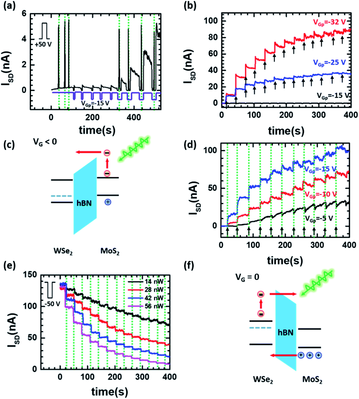 | ||
| Fig. 3 (a) ISD measured at VSD = +1 V when 532 nm laser pulses, VGp = −15 V, or 532 nm-laser pulses with VGp = −15 V were applied after applying VGp = +50 V. The dotted lines indicate when the laser pulses were applied. (b) ISD measured at VSD = +1 V when VGp = +50 V was applied to switch the device to the off state and then, VGp = −15, −25, or −32 V was repeatedly applied. The arrows indicate the time at which VGp was applied. (c) Energy band diagram proposed to explain the positive stepwise photoconductance. (d) ISD measured at VSD = +1 V when VGp = +50 V was applied to switch to the off state and then, 532 nm laser pulses (13 nW) and VGp = −5, −10, or −15 V were simultaneously applied. The dotted lines indicate when the laser pulses were applied, while the arrows indicate the time at which VGp was applied. (e) ISD measured at VSD = +1 V when VGp = −50 V was applied to switch the device to the on state and then, 532 nm laser pulses with a pulse width of 0.1 s and different powers were applied every 30 s. The dotted lines indicate the time when the laser pulses were applied. (f) Energy band diagram proposed to explain the negative stepwise photoconductance by light. | ||
To facilitate the trapping of holes in the MoS2 layer, the device was illuminated with 532 nm laser pulses while VG = −15 V was applied (Fig. 3(a)). Although the tunnel barrier is not sufficiently low, electrons are excited upon illumination and can tunnel from the MoS2 floating gate to the WSe2 channel (Fig. 3(c)). Consequently, more electrons are released from and holes become trapped in the MoS2 floating gate, leading to an increase in ISD at VSD = +1 V. When the device was irradiated with light pulses with VGp = −15 V, ISD returned to a value higher than the initial value in the dark at VG = 0 V, supporting that photoexcited electrons can tunnel from the MoS2 layer to the WSe2 channel by illumination with light pulses and VGp = −15 V. Fig. 3(d) shows ISD measured at VSD = +1 V when various values of VGp < 0 and 532 nm laser pulses with a width of 0.1 s and a power of 13 nW were simultaneously applied at the off state. ISD increased stepwise even with VGp = −5 V, indicating that positive stepwise photoconductance can be obtained by the simultaneous application of small negative VGp and laser pulses. Moreover, these optoelectronic multilevel states were dependent on the laser power and wavelength (Fig. S3†).
Next, the device was switched to the on state at ISD = +1 V by applying VGp = −50 V, which induced trapping of holes in the MoS2 layer and led to n-type behaviors. Then, ISD was measured at VSD = +1 V, while a 532 nm laser was repeatedly turned on for 0.1 s and then turned off for 30 s (Fig. 3(e)). Interestingly, ISD exhibited a stepwise decrease upon repeated exposure to laser pulses, and it decreased more rapidly with increasing laser power. This negative stepwise photoconductance can be explained by the tunneling of photoexcited electrons from the WSe2 channel to the MoS2 floating gate or the tunneling of holes from the MoS2 floating gate to the WSe2 channel, because the application of VGp = −50 V lowered the tunneling barrier to allow photoexcited electrons to tunnel from the WSe2 to the MoS2 (Fig. 3(f)). Similar measurements were performed upon repeated illumination with laser pulses with different exposure times and wavelengths (Fig. S4†). As the exposure time increased or the laser wavelength decreased, the ISD decreased more rapidly owing to an increase in the number of photoexcited electrons.
To switch the device to the on state at VSD < 0, VGp = +50 V was applied, which led to p-type behaviors. Upon repeated illumination with 635 nm laser pulses, the ISD measured at VSD = −1 V exhibited a stepwise negative photoconductance (Fig. S5(a)†). In this case, the tunneling barrier was lowered to allow photoexcited electrons to tunnel from the MoS2 to the WSe2 (Fig. S5(b)†); thus, illumination with laser pulses resulted in a decrease in |ISD| at VSD = −1 V. Although MoS2 is nearly transparent, more photoexcited electrons might be created in the MoS2 top layer than in the WSe2 channel during irradiation. Thus, compared to the results with VGp = −50 V and VSD = +1 V, a similar stepwise decrease in ISD was obtained using laser pulses with a longer wavelength.
Application of rectifying optoelectronic memory devices to optoelectronic synapse devices
Fig. 4(a) shows the ISD measured at VSD = +1 V, when VGp = −10 V and 532 nm laser pulses (width of 1 s, power of 54 nW) were repeatedly and simultaneously applied after applying VGp = +50 V. ISD exhibited 128 optoelectronic memory states. Subsequently, for depression, VGp = +11 V and 635 nm laser pulses with a width of 0.03 s and a power of 1 nW were simultaneously applied. Although ISD was decreased by 532 nm laser pulses without VGp (Fig. 3(e)), more symmetric potentiation and depression curves could be obtained by the application of VGp = +11 V and 635 nm laser pulses. Fig. 4(b) shows the normalized conductance change (ΔS/S0) measured at VSD = +1 V after applying a 10-pulse train with an amplitude of −30 V and different spacing times (Δt) to VG. As Δt decreased, ΔS/S0 increased, implying that STDP can be realized using this device. We also performed theoretical learning and recognition tasks using an ANN with a size of 784 × 10 based on the SLP model. The recognition rate was estimated to be approximately 72%, which is comparable to the previously reported values (Fig. 4(e)).38–40 | ||
| Fig. 4 (a) ISD measured at VSD = +1 V for the WSe2-based device with the MoS2 top layer when VGp = +50 V was applied to switch the device to the off state and then, potentiation pulses (532 nm laser pulses (54 nW, 1 s) and VGp = −10 V) and depression pulses (635 nm laser pulses (1 nW, 0.03 s) and VGp = +11 V) were repeatedly applied. The insets show enlarged plots. Green and red dotted lines indicate the times when 532 nm and 635 nm laser pulses were applied, respectively, and the arrows indicate when VGp was applied. (b) Normalized conductance change (ΔS/S0) measured at VSD = +1 V after a 10 pulse train with an amplitude of −30 V and different spacing times (Δt) was applied to VG, demonstrating spike-rate-dependent plasticity. (c) PSC measured according to number of pulses applied. The NL was estimated to be 0.5 and 4.2 for potentiation and depression, respectively. (d) Schematic of ANN model for analyzing post synaptic learning and recognizing processes of the device. (e) Recognition rate according to the number of learning processes. | ||
In addition to the WSe2/graphene device with the MoS2 top layer, we fabricated a device with a WSe2 top layer. It also exhibited gate-tunable rectification inversion, rectified nonvolatile memory properties, and multilevel optoelectronic memory effects (Fig. S6†). Furthermore, quite symmetric and linear potentiation and depression processes could be implemented using single-wavelength laser pulses with different powers (Fig. S7†). The NL was estimated to be 1.0 and 0.6 for potentiation and depression, respectively, which is more symmetric in comparison with the device with the MoS2 top layer. These results suggest that the linearity and symmetry of the potentiation and depression curves may be improved by controlling the energy band structure.
Application of rectifying memory effects to mimicking excitatory and inhibitory synapses
The indicating that hole or electron tunneling can occur depending on the polarity of VGp suggests that this device may be applied to mimic excitatory and inhibitory synapses that involve different neurotransmitters. Glutamate is the most common neurotransmitter for excitatory synapses that brings the membrane potential of the postsynaptic neuron toward the threshold for generating action potentials, whereas GABA is the neurotransmitter for inhibitory synapses that drive the membrane potential of the postsynaptic neuron away from the threshold for generating action potentials.41,42 To explore the feasibility of mimicking excitatory and inhibitory synapses, two similar devices were connected in parallel, as shown in Fig. 5(a). When VGp = −60 or +60 V was applied to both devices, the I–V curves showed rectifying characteristics with increasing current (Fig. S8(a) and (b)†). However, when VGp = −60 V was applied to one device and VGp = +60 V to the other device, the I–V curve was almost symmetric (Fig. S8(c)†). | ||
| Fig. 5 (a) A circuit consisting of two devices (A and B) connected in parallel (top) and a schematic of excitatory and inhibitory synapses connected to a postneuron (bottom). I measured at V of ±1 V square waves with a frequency of 5 Hz when VGp = −60 V was applied to device A, followed by repeatedly applying (b) VGp = −40 V or (c) VGp = +40 V to device B. | ||
Fig. 5(b) and (c) show I measured at V of ±1 V square waves when VGp = −60 V was applied to device A, followed by repeatedly applying VGp = −40 and +40 V for 0.1 s to device B, respectively. Upon the application of VGp = −60 V to device A, rectified I was measured and its value was nearly unchanged due to the nonvolatile memory effects. Subsequently, when VGp = −40 V was repeatedly applied to device B, I gradually increased and the rectifying characteristics were maintained. In contrast, when VGp = +40 V was repeatedly applied to device B, I gradually decreased. We also performed similar measurements, in which VGp = +60 V was applied to device A and then VGp = −40 or +40 V was repeatedly applied to device B. Similar behaviors were observed although the polarity of I was changed (Fig. S9(a) and (b)†). These results demonstrate that the application of VGp = −40 and +40 V causes effects similar to activating excitatory and inhibitory synapses, respectively.
Conclusions
We fabricated WSe2/graphene heterostructures with a photoresponsive floating gate of MoS2 or WSe2, and investigated their multifunctional properties including gate-controlled rectification inversion, rectified nonvolatile memory effects with an on/off ratio of 104 and a retention time >103 s, and multilevel optoelectronic memory effects. When VGp ≪ 0 was applied, the device was switched to the on state at VSD > 0 and the off state at VSD < 0 as electrons were trapped in the floating gate. In contrast, when VGp ≫ 0 was applied, the device was switched to the off state at VSD > 0 and to the on state at VSD < 0 as holes were trapped in the floating gate. Furthermore, upon repeated illumination with laser pulses, ISD decreased or increased stepwise depending on the history of VGp, which was ascribed to the tunneling of photoexcited electrons between the WSe2 channel and the floating gate through the hBN layer via the Fowler–Nordheim tunneling mechanism. In particular, 128 optoelectronic memory states with the NL < 1 could be achieved, suggesting that these multifunctional devices can be applied to optoelectronic synapse devices. Learning and recognition tasks were also performed using the ANN based on SLP model and the recognition rate was calculated to be approximately 72%. In addition, we demonstrated that WSe2/graphene heterostructures with a floating gate may be applied to artificial synaptic devices that emulate inhibitory as well as excitatory synapses.Experimental section
Device fabrication
Devices were fabricated, as shown in Fig. S10.† First, hBN flakes (15–21 nm) were mechanically exfoliated from an hBN single crystal (HQ graphene) using scotch tape and a selected hBN flake (∼11 nm) was transferred onto a SiO2/Si substrate using a polydimethylsiloxane (PDMS) stamping method. The Au electrode (50 nm) was fabricated using electron-beam lithography and lift-off techniques and the graphene electrode (∼15 nm) was made by transferring a graphene flake (HQ graphene) onto the hBN. Next, a WSe2 flake (∼10 nm) was transferred onto the prepared electrodes, resulting in a WSe2 field-effect transistor (FET). After heating at 85 °C for 30 min on a hot plate, the FET was characterized. Subsequently, hBN (∼11 nm) and MoS2 (∼11 nm) flakes were transferred onto the WSe2 FET, and polystyrene was spin-coated to improve the contact between the vdW materials. WSe2 and MoS2 flakes were exfoliated from commercially available crystals (2D semiconductors).Measurements
To characterize their optoelectronic properties, the devices were placed in a homemade vacuum chamber with an optical window. Electrical measurements were carried out using a semiconductor characterizer (4200-SCS, Keithley). Laser pulses were applied through the optical window and the exposure time was controlled using an optical shutter (SB5/M Aperture and SC10 controller, Thorlabs). SKPM images were acquired using an atomic force microscope (Park NX10, Park System) with a Cr–Au conducting cantilever.Weight update method
A large-scale neural network with a size of 784 × 10 were constructed theoretically based on the single-layer perceptron model. The hand-written images of the MNIST database were pixelated with 255 levels of black and white contrast and then input as a form of a voltage matrix (V1 − Vi, V). This input voltage was multiplied by a synaptic weight vector (W1,1 − Wi,j, W) to be converted to an output current vector (I1 − Ij = ∑Vi × Wij). Here, the synaptic weight refers to the difference (W = G+ − G−) between the conductance state of potentiation (G+) and depression (G−) regions of the LTP/LTD curve. Next, the net current (netj) collected at the output neuron was converted using the sigmoid function (ƒ(netj)) to have values between “0” and “1”. The ƒ(netj) was then subtracted to a label value (kj) to define the weight-update determining factor ‘δj’ (δj = kj − ƒ(netj)). Finally using a sign function, when sgn(δj × Vi) was positive, we increased the synaptic weight between ith input neuron and jth output neuron and decreased the corresponding synaptic weights when sgn(δj × Vi) was negative. Finally, weight update was not processed when sgn(δj × Vi) is 0.Author contributions
S. H. Kim proposed the idea, design the experiments and wrote the manuscript, M. U. Park, C. J. Lee and S. G. Yi helped perform electric and optical measurements, M. Kim helped optimize the scheme and figures and Y. Choi performed the SLP simulation.Conflicts of interest
There are no conflicts to declare.Acknowledgements
This work has been financially supported by the Basic Science Research Program through the National Research Foundation of Korea (NRF) (Grant No. 2019R1H1A2080077 and 2020R1A202011942).Notes and references
- A. K. Geim and I. V. Grigorieva, Nature, 2013, 499, 419–425 CrossRef CAS PubMed.
- M. Y. Li, C. H. Chen, Y. Shi and L. J. Li, Mater. Today, 2016, 19, 322–335 CrossRef CAS.
- L. Lv, J. Yu, M. Hu, S. Yin, F. Zhuge, Y. Ma and T. Zhai, Nanoscale, 2021, 13, 6713–6751 RSC.
- M. Huang, S. Li, Z. Zhang, X. Xiong, X. Li and Y. Wu, Nat. Nanotechnol., 2017, 12, 1148–1154 CrossRef CAS PubMed.
- R. Cheng, F. Wang, L. Yin, Z. Wang, Y. Wen, T. A. Shifa and J. He, Nat. Electron., 2018, 1, 356–361 CrossRef CAS.
- R. Cheng, F. Wang, L. Yin, K. Xu, T. A. Shifa, Y. Wen, X. Zhan, J. Li, C. Jiang, Z. Wang and J. He, Appl. Phys. Lett., 2017, 110, 173507 CrossRef.
- M. Massicotte, P. Schmidt, F. Vialla, K. G. Schädler, A. Reserbat-Plantey, K. Watanabe, T. Taniguchi, K. J. Tielrooij and F. H. L. Koppens, Nat. Nanotechnol., 2016, 11, 42–46 CrossRef CAS PubMed.
- Y. Chen, J. Yu, F. Zhuge, Y. He, Q. Zhang, S. Yu, K. Liu, L. Li, Y. Ma and T. Zhai, Mater. Horiz., 2020, 7, 1331–1340 RSC.
- M. D. Tran, H. Kim, J. S. Kim, M. H. Doan, T. K. Chau, Q. A. Vu, J. H. Kim and Y. H. Lee, Adv. Mater., 2019, 31, 1807075 CrossRef PubMed.
- S. H. Kim, S. G. Yi, M. U. Park, C. Lee, M. Kim and K. H. Yoo, ACS Appl. Mater. Interfaces, 2019, 11, 25306–25312 CrossRef CAS PubMed.
- S. H. Yang, K. C. Lee, M. Y. Tsai, Y. M. Chang, C. Y. Lin, F. S. Yang, K. Watanabe, T. Taniguchi, C. H. Lien, C. H. Ho, M. Li, Y. F. Lin and Y. C. Lai, Nano Energy, 2019, 66, 104107 CrossRef CAS.
- A. Gao, E. Liu, M. Long, W. Zhou, Y. Wang, T. Xia, W. Hu, B. Wang and F. Miao, Appl. Phys. Lett., 2016, 108, 223501 CrossRef.
- R. Ge, X. Wu, M. Kim, J. Shi, S. Sonde, L. Tao, Y. Zhang, J. C. Lee and D. Akinwande, Nano Lett., 2018, 18, 434–441 CrossRef CAS PubMed.
- Y. Shi, X. Liang, B. Yuan, V. Chen, H. Li, F. Hui, Z. Yu, F. Yuan, E. Pop, H. S. P. Wong and M. Lanza, Nat. Electron., 2018, 1, 458–465 CrossRef.
- R. Xu, H. Jang, M. H. Lee, D. Amanov, Y. Cho, H. Kim, S. Park, H. J. Shin and D. Ham, Nano Lett., 2019, 19, 2411–2417 CrossRef CAS PubMed.
- L. Wang, Z. Wang, W. Zhao, B. Hu, L. Xie, M. Yi, H. Ling, C. Zhang, Y. Chen, J. Lin, J. Zhu and W. Huang, Adv. Electron. Mater., 2017, 3, 1600244 CrossRef.
- H. Tian, W. Mi, X. F. Wang, H. Zhao, Q. Y. Xie, C. Li, Y. X. Li, Y. Yang and T. L. Ren, Nano Lett., 2015, 15, 8013–8019 CrossRef CAS PubMed.
- W. Huh, S. Jang, J. Y. Lee, D. Lee, D. Lee, J. M. Lee, H. G. Park, J. C. Kim, H. Y. Jeong, G. Wang and C. H. Lee, Adv. Mater., 2018, 30, 1801447 CrossRef PubMed.
- H. Tian, X. Cao, Y. Xie, X. Yan, A. Kostelec, D. Dimarzio, C. Chang, L. D. Zhao, W. Wu, J. Tice, J. J. Cha, J. Guo and H. Wang, ACS Nano, 2017, 11, 7156–7163 CrossRef CAS PubMed.
- V. K. Sangwan, H. S. Lee, H. Bergeron, I. Balla, M. E. Beck, K. S. Chen and M. C. Hersam, Nature, 2018, 554, 500–504 CrossRef CAS PubMed.
- S. G. Yi, M. U. Park, S. H. Kim, C. J. Lee, J. Kwon, G. H. Lee and K. H. Yoo, ACS Appl. Mater. Interfaces, 2018, 10, 31480–31487 CrossRef CAS PubMed.
- F. Zhou, Z. Zhou, J. Chen, T. H. Choy, J. Wang, N. Zhang, Z. Lin, S. Yu, J. Kang, H. S. P. Wong and Y. Chai, Nat. Nanotechnol., 2019, 14, 776–782 CrossRef CAS PubMed.
- C. Li, M. Hu, Y. Li, H. Jiang, N. Ge, E. Montgomery, J. Zhang, W. Song, N. Dávila, C. E. Graves, Z. Li, J. P. Strachan, P. Lin, Z. Wang, M. Barnell, Q. Wu, R. S. Williams, J. J. Yang and Q. Xia, Nat. Electron., 2018, 1, 52–59 CrossRef.
- T. Ahmed, M. Tahir, M. X. Low, Y. Ren, S. A. Tawfik, E. L. H. Mayes, S. Kuriakose, S. Nawaz, M. J. S. Spencer, H. Chen, M. Bhaskaran, S. Sriram and S. Walia, Adv. Mater., 2021, 33, 2004207 CrossRef CAS PubMed.
- T. G. Smart, Curr. Opin. Neurobiol., 1997, 7, 358–367 CrossRef CAS PubMed.
- A. B. Brussaard, K. S. Kits and T. A. de Vlieger, J. Physiol., 1996, 497(2), 495–507 CrossRef CAS PubMed.
- M. A. Howard and E. W. Rubel, J. Neurosci., 2010, 30, 12063–12074 CrossRef CAS PubMed.
- W. Truccolo, J. A. Donoghue, L. R. Hochberg, E. N. Eskandar, J. R. Madsen, W. S. Anderson, E. N. Brown, E. Halgren and S. S. Cash, Nat. Neurosci., 2011, 14, 635–643 CrossRef CAS PubMed.
- Y. Liu, J. Guo, E. Zhu, L. Liao, S. J. Lee, M. Ding, I. Shakir, V. Gambin, Y. Huang and X. Duan, Nature, 2018, 557, 696–700 CrossRef CAS PubMed.
- C. M. Went, J. Wong, P. R. Jahelka, M. Kelzenberg, S. Biswas, M. S. Hunt, A. Carbone and H. A. Atwater, Sci. Adv., 2019, 5, eaax6061 CrossRef CAS PubMed.
- X. X. Li, Z. Q. Fan, P. Z. Liu, M. L. Chen, X. Liu, C. K. Jia, D. M. Sun, X. W. Jiang, Z. Han, V. Bouchiat, J. J. Guo, J. H. Chen and Z. D. Zhang, Nat. Commun., 2017, 8, 970 CrossRef PubMed.
- C. Wang, S. Yang, W. Xiong, C. Xia, H. Cai, B. Chen, X. Wang, X. Zhang, Z. Wei, S. Tongay, J. Li and Q. Liu, Phys. Chem. Chem. Phys., 2016, 18, 27750–27753 RSC.
- W. Liu, J. Kang, D. Sarkar, Y. Khatami, D. Jena and K. Banerjee, Nano Lett., 2013, 13, 1983–1990 CrossRef CAS PubMed.
- D. S. Schulman, A. J. Arnold and S. Das, Chem. Soc. Rev., 2018, 47, 3037–3058 RSC.
- R. Yan, Q. Zhang, W. Li, I. Calizo, T. Shen, C. A. Richter, A. R. Hight-Walker, X. Liang, A. Seabaugh, D. Jena, H. Grace Xing, D. J. Gundlach and N. V. Nguyen, Appl. Phys. Lett., 2012, 101, 022105 CrossRef.
- M. Tello, M. Chiesa, C. M. Duffy and H. Sirringhaus, Adv. Funct. Mater., 2008, 18, 3907–3913 CrossRef CAS.
- T. Hallam, C. M. Duffy, T. Minakata, M. Ando and H. Sirringhaus, Nanotechnology, 2009, 20, 025203 CrossRef CAS PubMed.
- Y. Choi, J. H. Kim, C. Qian, J. Kang, M. C. Hersam, J. H. Park and J. H. Cho, ACS Appl. Mater. Interfaces, 2020, 12, 4707–4714 CrossRef CAS PubMed.
- J. Sun, S. Oh, Y. Choi, S. Seo, M. J. Oh, M. Lee, W. B. Lee, P. J. Yoo, J. H. Cho and J. H. Park, Adv. Funct. Mater., 2018, 28, 1804397 CrossRef.
- S. Kim, B. Choi, M. Lim, J. Yoon, J. Lee, H. D. Kim and S. J. Choi, ACS Nano, 2017, 11, 2814–2822 CrossRef CAS PubMed.
- B. S. Meldrum, J. Nutr., 2000, 130, 1007S–1015S CrossRef CAS PubMed.
- D. F. Owens and A. R. Kriegstein, Nat. Rev. Neurosci., 2002, 3, 715–727 CrossRef CAS PubMed.
Footnote |
| † Electronic supplementary information (ESI) available. See DOI: 10.1039/d1na00504a |
| This journal is © The Royal Society of Chemistry 2021 |