
 Open Access Article
 This Open Access Article is licensed under a Creative Commons Attribution-Non Commercial 3.0 Unported Licence
Materials design of vertically coupled plasmonic arrays†
Goekalp Engin
Akinoglu
 *ab,
Eser Metin
Akinoglu
c,
Krzysztof
Kempa
d and
James Andell
Hutchison
*a
*ab,
Eser Metin
Akinoglu
c,
Krzysztof
Kempa
d and
James Andell
Hutchison
*a
aSchool of Chemistry, University of Melbourne, Parkville, Victoria, 3010, Australia. E-mail: engina@zedat.fu-berlin.de; james.hutchison@unimelb.edu.au
bAdvanced Materials & BioEngineering Research Centre (AMBER), The School of Chemistry, Trinity College Dublin, The University of Dublin, Dublin 2, Ireland
cInternational Academy of Optoelectronics at Zhaoqing, South China Normal University, Zhaoqing, 526238 Guangdong, China
dBoston College, Department of Physics, Chestnut Hill, MA 02467, USA
First published on 12th October 2021
Abstract
Plasmonic metasurfaces have important applications in life science, optics, and catalysis. However, their industrial usage is limited by the challenges of high throughput nanofabrication. A promising solution is the transfer of a pattern into a substrate using block copolymers, nanostructured stamps or molds to create binary, three dimensional templates, which can then be decorated with plasmonically active metals. Here, we report on the optical properties of quasi-Babinet complementary arrays in the non-retarded regime investigated by finite-difference time-domain simulations. The structures consist of a nanopillar support, which is covered with metal disks on top of the pillars and a quasi-Babinet complementary hole array film at the base of the pillars. Strong vertical plasmonic coupling occurs for small separation distances of the plasmonic slabs. We present a comprehensive study of the near and far-field properties of such vertically coupled plasmonic arrays varying their critical geometric dimension and the employed metals with their intrinsic plasmonic material properties. In particular, we consider gold, silver, copper, aluminum, nickel, and palladium. Furthermore, the effect of the refractive index n of the nanopillar support between the range of n = 1.4 to n = 3.4 is investigated. The plasmonic slabs show tunable extraordinary transmission and large electric near-field enhancements, which are strongly dependent on the employed material and geometry. Further, we show that the templates are suitable for plasmonic heterostructures commonly used in plasmon-enhanced photocatalysis.
1. Introduction
The cost effective fabrication of nanopillar templates by nanoimprint lithography,1,2 roll-to-roll nanoimprint processing,3,4 block copolymer lithography5 and hot embossing/nanoinjection moulding4,6 enable an effective route to create plasmonic metasurfaces on an industrial scale.7 Subsequently, a thin metal coating can be deposited onto the nanopillar template to create a plasmonic slab that consists of a hole array film at the base of the nanopillars and a quasi-Babinet complementary disk array on top of the nanopillars. The plasmonic properties of the template can be adjusted by the choice of metal and support material and the geometrical dimensions of the underlying structures.8 For small nanopillar aspect ratios the plasmon resonance of (i) the disk array, and (ii) the hole film can hybridize and couple vertically. The optical response of such vertically coupled plasmonic arrays (VCPAs) exhibits extraordinary optical transmission, which has been exploited to fabricate optical filters,9–11 refractive index sensors12–14 or plasmonic nanopixels beyond the diffraction limit.15–17 Further, small plasmonic junctions between the two plasmonic slabs of the VCPAs can drastically increase the local electric near-field. This effect has been used to increase sensitivity of spectroscopic instrumentation such as in surface-enhanced fluorescence spectroscopy,18,19 surface-enhanced Raman spectroscopy5,20 and surface-enhanced infrared spectroscopy.21Previously, we have shown that the plasmon resonance of VCPAs with hexagonal symmetry can be described as whispering gallery modes in the mid-infrared.8 In this regime the plasmon resonance is retarded and the plasmon dispersion follows the light line.22,23 As a consequence, the plasmon resonance is independent of the plasmonic material as long as the material is conductive.24 This changes drastically in the visible region of the electromagnetic spectrum where the plasmon resonance is non-retarded and deviates from the light line.22,23 In this regime the plasmon resonance is governed by Mie resonances, which are highly material dependent.23,24
The choice of the metal employed in the VCPAs is often specific to the intended application, where in addition to the metal's plasmonic properties, other aspects such as its abundance, stability to oxidation, biological compatibility, magneto-optical properties, and catalytic activity are important. Gold and silver are the most commonly employed plasmonic metals due to their excellent plasmon activity and stability, however they are expensive. Copper and aluminum are readily available but oxidize when in contact with air. A protective polymer coating can hinder this oxidation, however this blocks access to the metal surface where the plasmonic field is at its strongest. Nickel and palladium have received wide attention for their catalytic capabilities, but as plasmonic materials they face challenges such as high loss, and high expense, respectively. Here, we provide a comprehensive overview of the optical properties of VCPAs consisting of various plasmonic materials, dielectric supports, and geometrical dimensions, as simulated by finite-difference time-domain (FDTD) simulations. Such simulations are routinely used to predict and verify the optical behavior of experimentally fabricated plasmonic metasurfaces.1–6,8–23 Finally, we demonstrate that VCPAs can effectively form plasmonic heterostructures commonly used in plasmon-enhanced photocatalysis.
2. Results and discussion
2.1. Quasi-Babinet complementarity
Babinet's principle states that the transmittance Tλ of a slab and the transmittance of its complementary counterpart Tλ,c are related as:| Tλ + Tλ,c = 1 | (1) |
The principle assumes that the film thickness is infinitesimally small and does not account for absorption losses or coupling effects. Eqn (1) implies that the plasmon excitation energy of a disk array, and that of its complementary hole array should be identical. In Fig. 1A we have simulated the transmittance of hexagonally-arranged Au nanodisks on glass nanopillars with varying diameter. The plasmon resonances feature as a prominent dip in the region 515–630 nm, exhibiting a slight red shift with increasing particle size. This shift can be explained by the lower restoring force experienced by opposing charges as the disk diameter increases, resulting in a lower resonance energy of the localized surface plasmon.25 In the long wavelength limit the transmission approaches unity and in the short wavelength limit the slab shows reduced transmission due to the intrinsic absorption of Au, which scales with the fraction of Au covering the surface. In Fig. 1B the transmittance of the corresponding quasi-Babinet complementary hole array films at the base of the nanopillars is shown, and it indeed obeys approximately eqn (1). The spectra reveal extraordinary transmission (EOT)26 with peaks that are slightly red-shifted relative to their quasi-Babinet complementary counterparts in Fig. 1A. We attribute this slight red shift to the increased polarizability of the hole film's immediate environment, nevertheless, eqn (1) holds qualitatively even though absorption losses are not considered in the Babinet picture. This is further illustrated by the black continuous and dashed lines in Fig. 1B, which are 1−T plots of the 90 nm and 80 nm disk diameter array transmission spectra respectively from Fig. 1A.
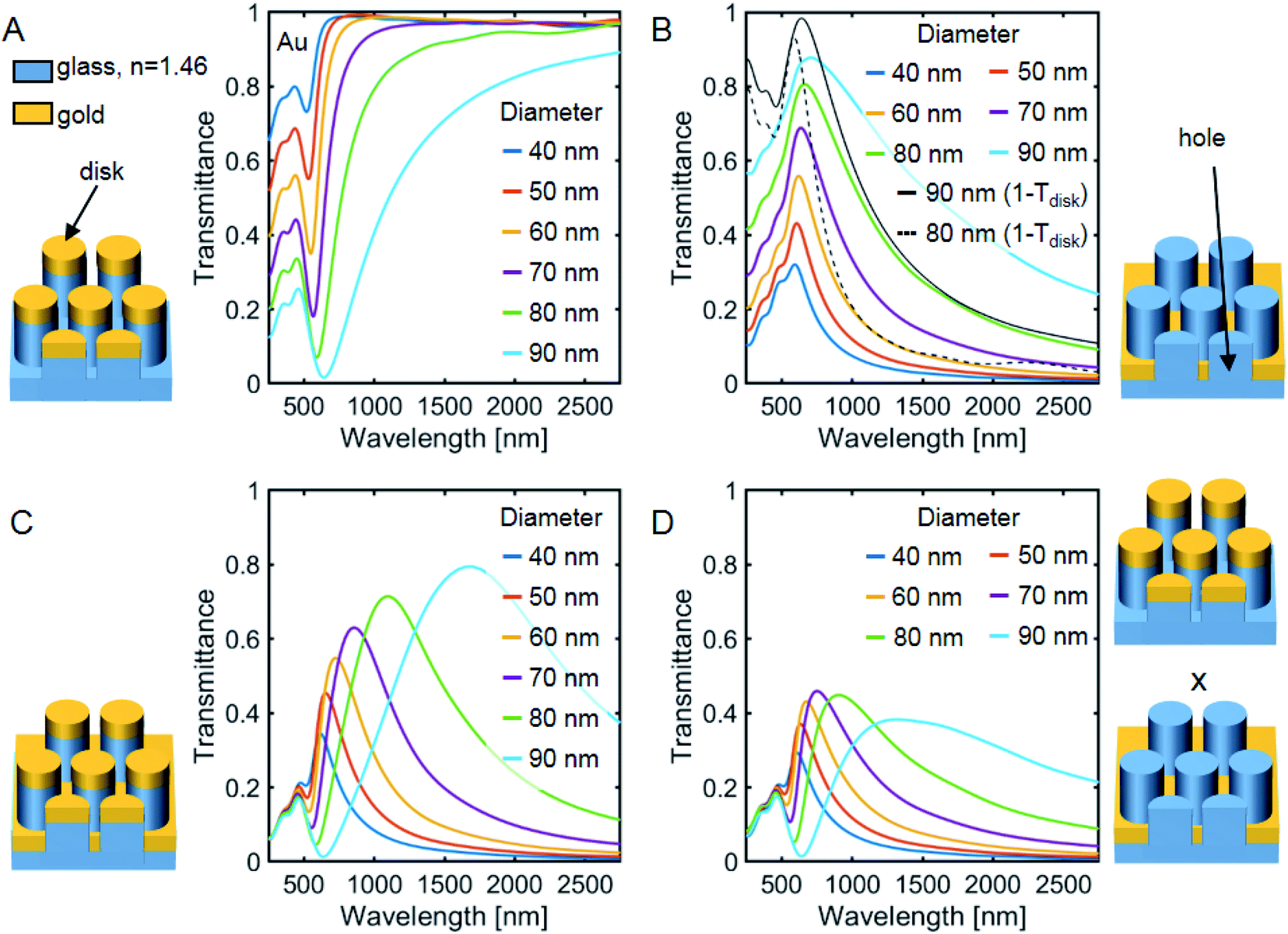 | ||
| Fig. 1 FDTD transmittance spectra of periodic plasmonic gold arrays on a nanopillar support with varying diameter and fixed height = 70 nm, pitch = 100 nm and gold thickness = 40 nm. The drawings on the sides show the simulated structures. (A) Nanopillar array with gold disks on top of the pillars. (B) Nanopillar array with hole film at the base of the pillars. The black continuous and dashed line display 1−T plots with 90 nm and 80 nm disk diameter arrays extracted from respective curves in panel A. (C) VCPAs; nanopillar arrays with gold disks on top of the pillars and hole film at the base of the pillars. (D) Multiplication of the respective spectra from (A) and (B). | ||
In Fig. 1C we show the corresponding VCPAs with the presence of both the Au disk and hole array slabs together. The EOT peak is highly symmetric, red-shifts and increases in transmission with pillar diameter. To understand the origin of this behavior, we assume that the transmittance through both the complementary disk and hole layers is given approximately by a simple product of the transmittances through individual arrays. This is expected, as the probability of a photon propagating through these two layers is given by the product of subsequent penetration probabilities. Indeed, the plots of Ttotal = TdiskThole presented in Fig. 1D, show an impressive resemblance to those in Fig. 1C. In particular, they exhibit EOT and a diameter dependent red-shift, underscoring the power of Babinet's principle. However, this simple approach ignores the fact that the pillars are only 70 nm in height, and therefore the complementary plasmonic arrays are in each other's near-field such that their plasmonic modes can hybridize.27 Furthermore, the VCPAs show a reduced spectral energy width compared to the hole film which is an important design factor for narrow bandpass filters (Fig. S1† shows the spectra in Fig. 1vs. eV instead of wavelength).28
2.2. Pitch, height and metal thickness
The results of Fig. 1 show that the pillar diameter is a significant parameter of the VCPA's plasmon resonance position. The variation of the other geometric parameters is investigated here. Fig. 2, panels A1–A3, show the effect of pillar height variation for a fixed pillar diameter (50 nm) and array pitch (100 nm). There is a slight red shift of the VCPA EOT peak for shorter pillar heights. This is in agreement with the plasmon hybridization model, which predicts for the bonding modes a red shift for decreasing plasmonic gaps.27 The absorption spectra (panel A2) reveal two absorption modes at 525 nm and at 670 nm for a 5 nm vertical gap (pillar height). The two peaks blue-shift for larger pillar heights, where the lower energetic mode experiences a larger shift. Eventually the two peaks overlap for larger gaps and reduced vertical coupling. A similar behavior has been observed for the plasmon excitation of the dipolar and quadrupolar modes in nanoshell arrays caused by a different degree of hybridization.29 Panel A3 shows the electric near-fields plotted as a function of the wavelength. The respective electric near-field maxima with frequency ωNF occur at lower excitation frequency than the respective far-field absorption at frequency ωFF. This can be explained by a simple driven and damped harmonic oscillator model and directly depends on the total damping (radiative plus intrinsic) γ of the system,30 as follows .30 The shift between near- and far field response for traditional plasmonic materials in the visible spectral region is of the order of up to ∼100 nm.31 The near-field spectra reveal a strong vertical coupling between the disk array and the hole film, largest for the smallest vertical gap.
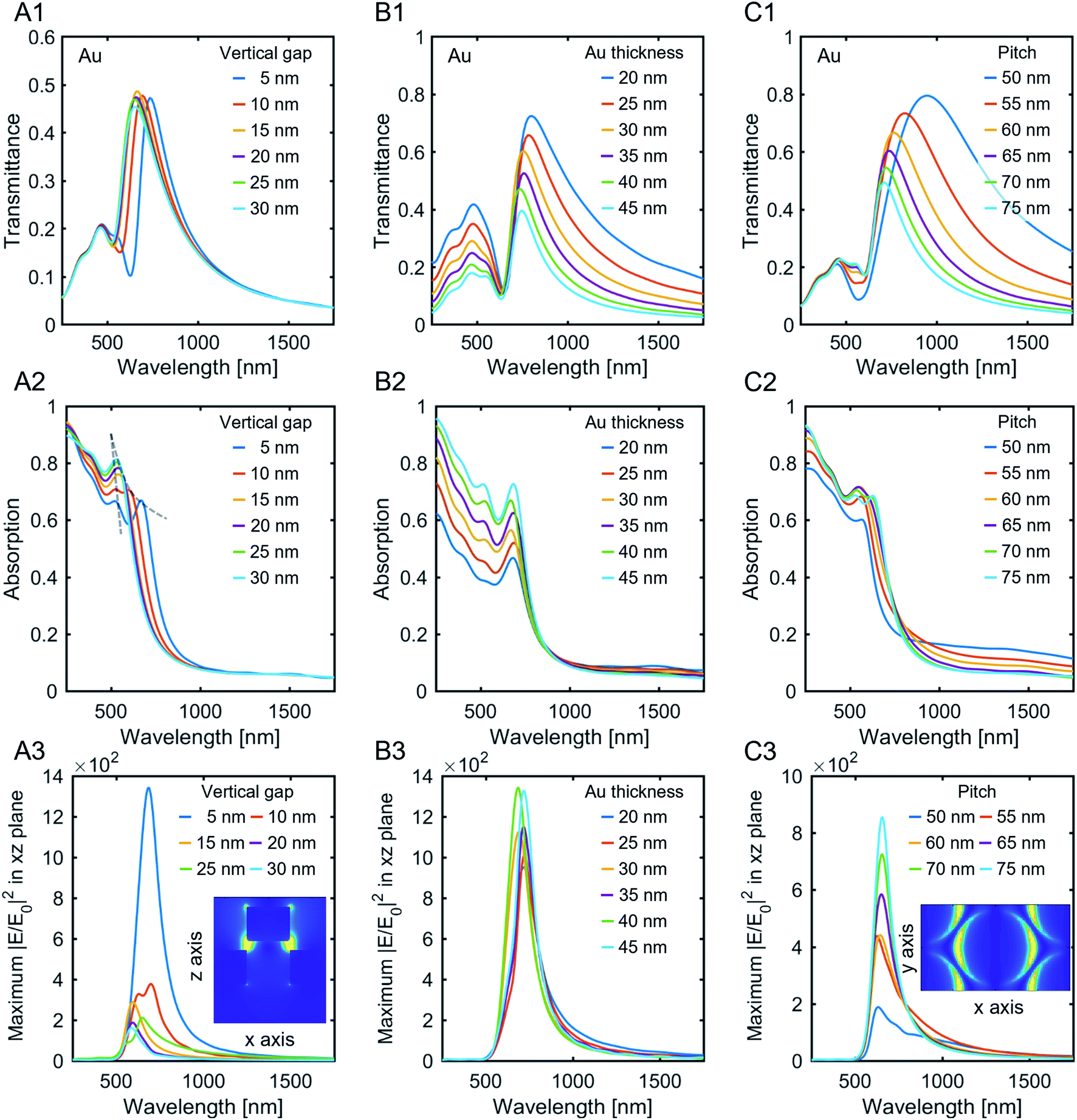 | ||
| Fig. 2 Au-based VCPAs with varying pillar height, metal film thickness, and array pitch. (A) Variation of the vertical gap (pillar height) with fixed pitch = 100 nm, diameter = 50 nm and Au thickness = 40 nm. (A1) Transmission spectra, (A2) absorption spectra where the grey dashed lines provide a guide for the eye for the shift of the two modes, and (A3) electric near-field enhancement. The inset shows the cross-section map at the plasmon resonance for a 10 nm vertical gap between the disks and holes for x-axis polarization. (B) Variation of the Au thickness with fixed pitch = 100 nm, diameter = 50 nm and vertical plasmonic gap = 5 nm. (B1) Transmission spectra, (B2) absorption spectra and (B3) electric near-field enhancement. (C) Variation of the pitch with fixed height = 45 nm, diameter = 40 nm and Au thickness = 40 nm. (C1) Transmission spectra, (C2) absorption spectra and (C3) electric near-field enhancement. The inset shows the in-plane map 1 nm above the hole film at the plasmon resonance for a 10 nm lateral gap between the pillars for x-axis polarization. | ||
The effect of metal film thickness at a constant 5 nm vertical gap between the hole film and the disk array is illustrated in Panels B1–B3 (again for a fixed pillar diameter of 50 nm and fixed array pitch of 100 nm). It has only a small effect on the plasmonic response. An increase in the metal thickness shows a slight blue shift in the resonance position because the polarizability of the material increases.32
Finally, the variation of the array pitch is examined in Panels C1–C3 (fixed pillar height and diameter of 45 nm and 40 nm respectively, and Au thickness of 40 nm). A strong red shift is predicted as the pitch approaches the nanopillar diameter, i.e. for a smaller lateral gap, as interpillar coupling becomes important. While the electric near-field enhancement increases with the pitch, the absorbance only weakly depends on the pitch.
2.3. Plasmonic metals
The choice of metal strongly determines the plasmonic response in the non-retarded regime. Different metals have a different free carrier bulk plasma frequency, which depends on the density N of free charge carriers. | (2) |
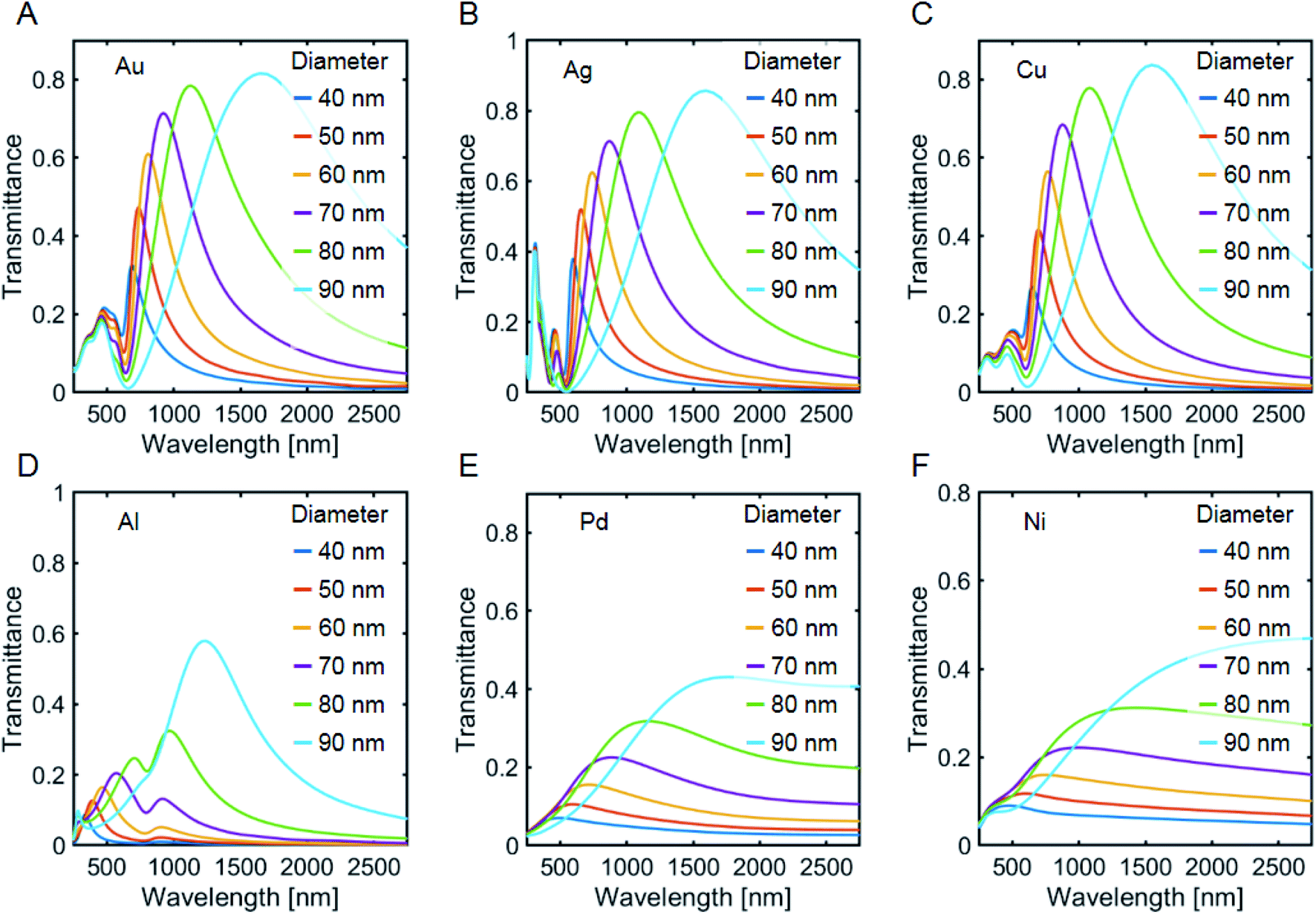 | ||
| Fig. 3 FDTD transmittance spectra of VCPAs made with different metal films (all 40 nm thick), with varying pillar diameter, fixed pillar height = 45 nm and fixed array pitch = 100 nm. (A) Au, (B) Ag, (C) Cu, (D) Al, (E) Pd and (F) Ni. | ||
The electric near-field spectra for VCPAs made with different metal films reveal that, as expected, the traditional plasmonic materials Au, Ag, Cu and Al, have a larger maximum enhancement factor for smaller disk/hole diameters (Fig. 4A–D). For small pillar diameters the two previously observed modes overlap and split up for larger diameters. However, the high energy mode exhibits only a small shift compared to the other lower energy modes. For larger diameters, a broader but weaker peak appears that corresponds to the plasmonic bonding mode. Ag VCPAs show the strongest near-field enhancement due to their low imaginary refractive index, in agreement with experimental surface-enhanced Raman studies.36 Pd and Ni feature significantly smaller near-field enhancement which is caused by their large damping factors (Fig. 4E and F).
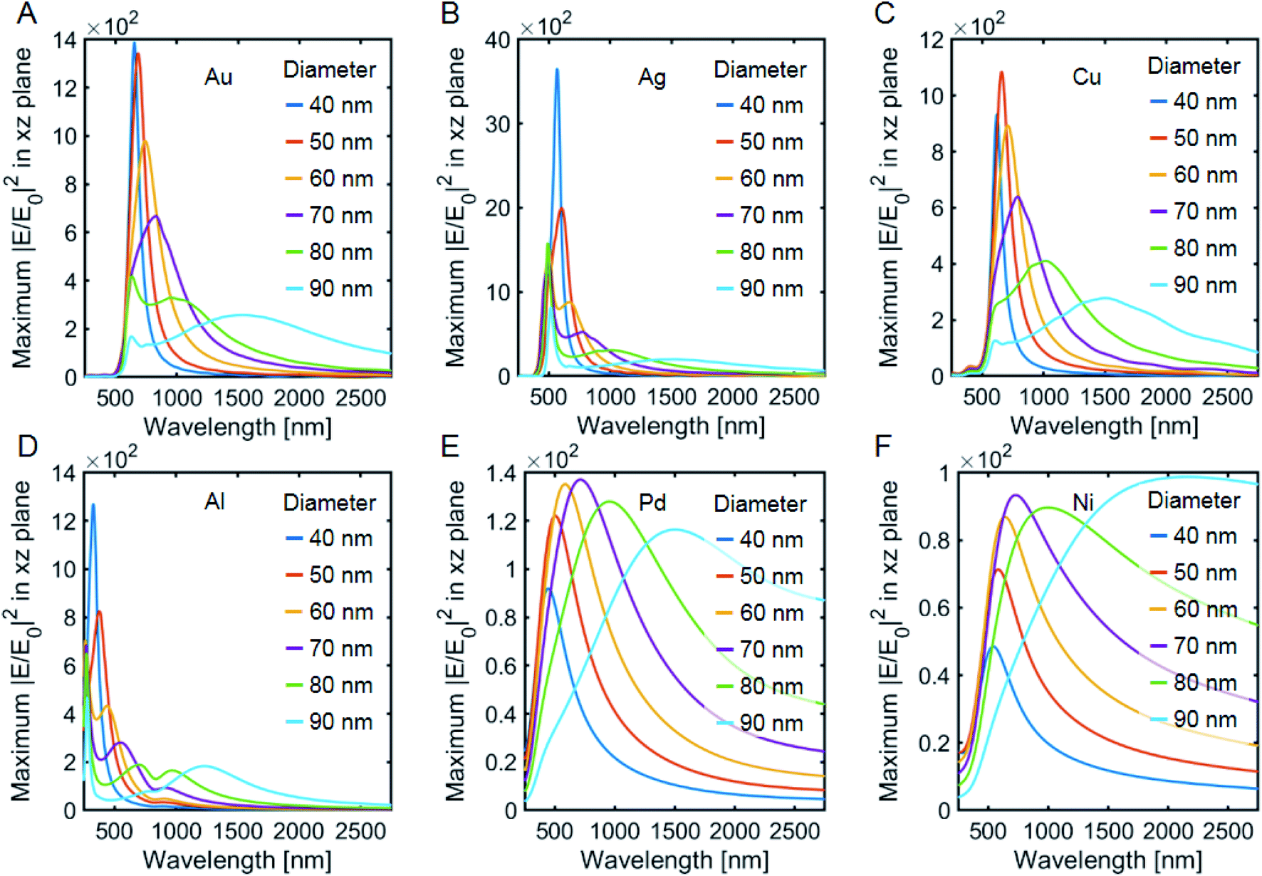 | ||
| Fig. 4 Simulated electric near-field enhancement of VCPAs made with different metal films (all 40 nm thick) at the cross-section plane with varying pillar diameter but fixed pillar height = 45 nm and fixed array pitch = 100 nm. (A) Au, (B) Ag, (C) Cu, (D) Al, (E) Pd and (F) Ni. | ||
2.4. Dielectric support
The plasmon resonance position is extremely sensitive to the dielectric environment of plasmonic nanostructure.12–14 This property is extensively used in surface plasmon resonance spectroscopy to detect binding events of biological macromolecules at the plasmonic template.14 Therefore, the refractive index of the substrate and the pillars is important. These effects are illustrated in Fig. 5. We investigated as substrate materials glass (n = 1.46), sapphire (n = 1.77), cubic zirconia (n = 2.16), titanium dioxide (n = 2.6) and silicon (n = 3.40). All these materials are optically transparent except silicon. The dielectric materials were simulated to be dispersionless and absorption losses of the substrate materials were not considered in the simulations. The plasmon resonance red shifts with increasing substrate refractive index, as expected (Fig. 5A and D). The line width and EOT wavelength maximum however are not significantly altered (Fig. 5A and B). The other metals show a similar behavior with a linear dependence of the wavelength maximum on the refractive index (Fig. 5B). The slopes for Pd and Ni are slightly steeper than for the other metals. The difference is attributed to their broader EOT maxima. The maximum transmission values of the EOT peaks also do not show a strong variation with refractive index for any of the metals studied (Fig. 5C). Fresnel reflection coefficients predict a five times higher reflection from an air–titanium dioxide interface than for an air–glass interface. However, the EOT does not show a significant variation for different refractive indices which illustrates a fundamental difference in the light–matter interaction based on the plasmonic activity.37 A highly polarizable substrate can be even beneficial to enhance the EOT.37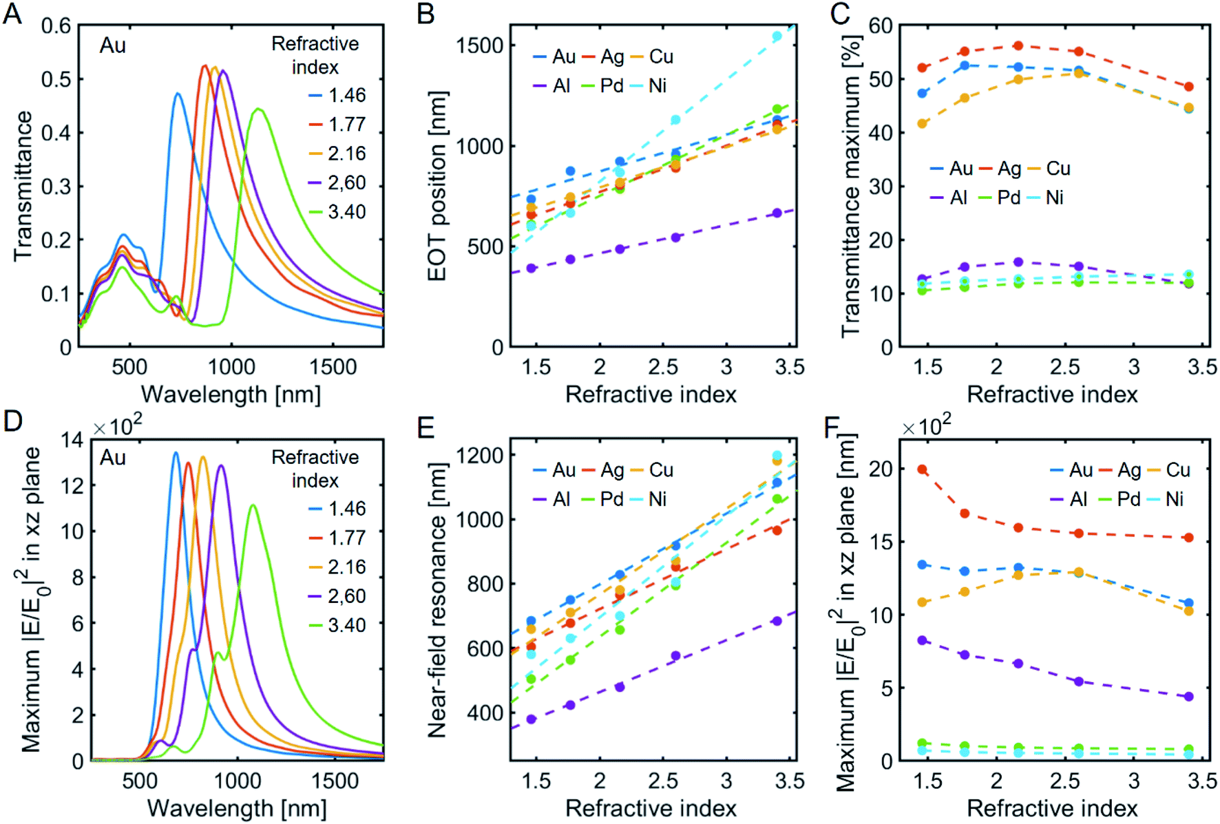 | ||
| Fig. 5 VCPAs using nanopillar materials with varying refractive index and fixed pitch = 100 nm, fixed pillar height = 45 nm, fixed metal thickness = 40 nm and fixed diameter = 50 nm. The materials simulated are glass (n = 1.46), sapphire (n = 1.77), cubic zirconia (n = 2.16), titanium dioxide (n = 2.6) and silicon (n = 3.40). (A) Au transmission spectra. (B) Change of the EOT peak position for different metals depending on the refractive index. (C) Respective maximum transmission values depending on the refractive index. (D) Electric near-field enhancement of Au. (E) Electric near-field resonance position for different metals versus the refractive index of the nanopillars. (F) Maximum electric near-field enhancement depending on the refractive index of the nanopillars. | ||
The near-field resonance wavelength is also linear with substrate refractive index for all the metals with similar slopes (Fig. 5E). Previously it was observed that the optical near-field could be reduced more than three times for planar plasmonic templates on high refractive substrate materials (nSi = 3.4) compared to on low refractive index substrates (nCaF2 = 1.3).38 It was suggested that placing plasmonic templates on nano-pedestals could overcome the electric screening by the substrate.39,40 However, our results indicate that the maximum electric near-field enhancement for VCPAs remains the same or is only slightly decreased for larger refractive index pillars (Fig. 5F). Furthermore, we observe for Cu a slight increase. Therefore, we conclude that the vertical plasmonic coupling alongside the air-substrate interface is robust towards substrate effects.
2.5. Plasmonic heterostructures
A promising strategy to increase the efficiency of conventional (photo)catalytic metals is to combine them with metals with a strong plasmonic response.41,42 This can be in either a core shell or bilayer configuration where the catalytic system consists of two or more different metals. Alternatively, the antenna-reactor geometry consists of a plasmonic antenna, which is excited optically and then transfers the energy to a proximal catalytic reaction site to facilitate a chemical reaction.43 The VCPAs provide a simple route to combine both these strategies by sequentially depositing two different metals on a nanopillar template. Ideally, the catalytic system should fully absorb light over a broad spectrum. The plasmon decay generates hot charge carriers that can subsequently participate in chemical reactions. It has also been reported that some reactions are even directly driven by strong electric near-fields.44 To explore the potential of bimetallic VCPAs as plasmonic heterostructures we have simulated two different series. First, we consider a situation where the nanopillars are coated first with Pd and then with Ag on top. Fig. 6A shows that the heterostructure shows a strong vertical coupling between the Pd disks and the Ag hole films. Absorption spectra reveal that the smaller diameter VCPAs can absorb up to 90% of the light (Fig. 6B) similar to the pure Pd VCPA counterpart (Fig. S2†). The electric near-field enhancement shows a more than one order of magnitude higher enhancement than for the pure Pd VCPAs which proves the superiority of the heterostructures. In the second case we consider the reverse geometry, i.e. Pd is deposited on top of Ag. Here, the plasmonic slabs shows strong coupling between the Pd hole film and the silver disks. Additionally, the Pd disks also show a strong electric near-field enhancement. The overall light absorption is similar to the first case where Ag was placed on top of Pd but the electric-near field enhancement is reduced by half. However, for catalytic applications, it is more feasible to place the Pd on top of Ag because in this configuration the surface area of the catalytically-active Pd is much larger.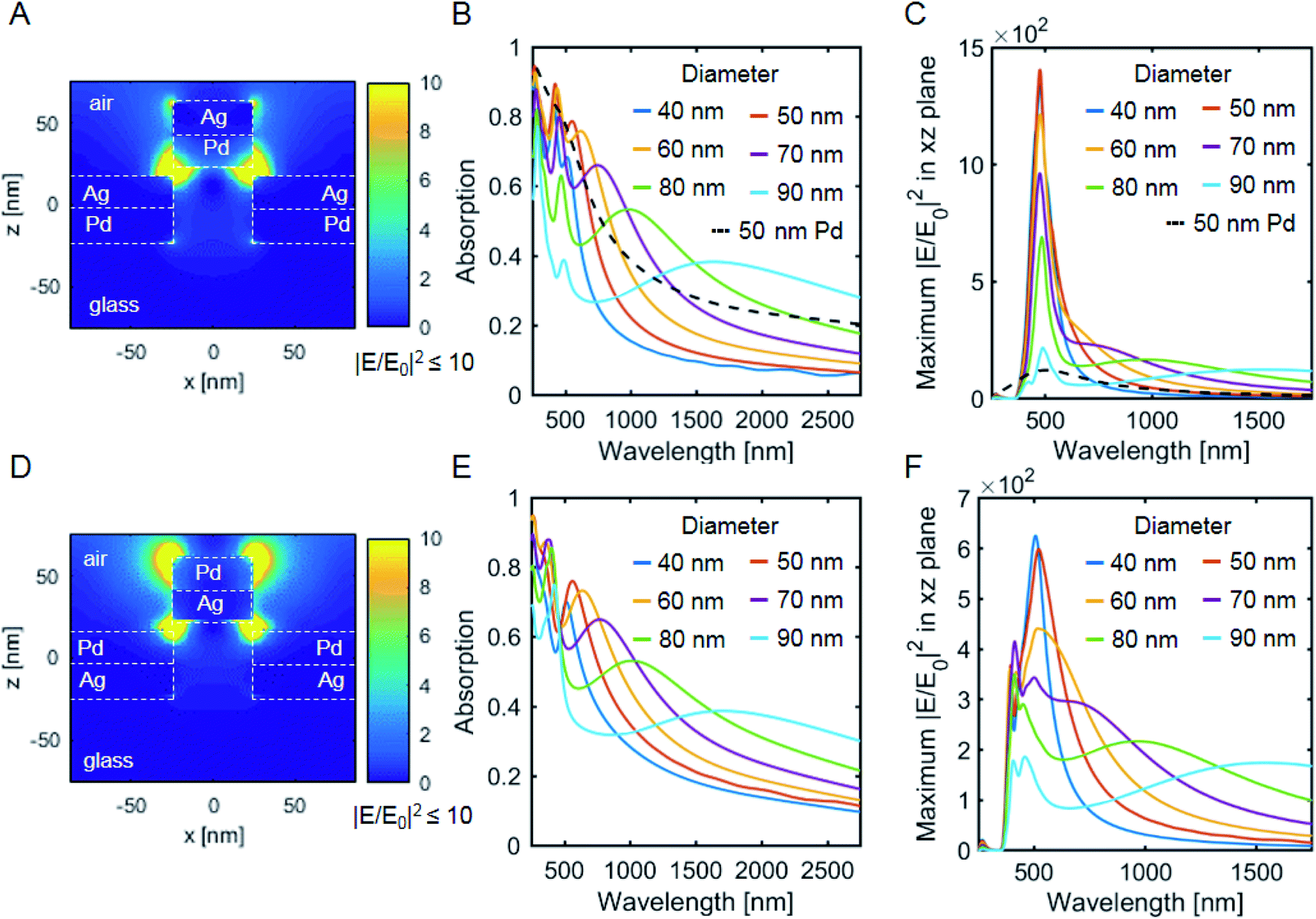 | ||
| Fig. 6 Metallic bilayers on glass nanopillars with pitch = 100 nm, metal thickness = 40 nm and pillar height 45 nm. (A–C) Ag on top of Pd. (A) Cross section with 50 nm diameter. (B) Absorption spectra and (C) electric near-field enhancement with varying diameter. The black dotted lines are the respective spectra for pure Pd and 50 nm pillar diameter. (D–F) Pd on top of Ag. (D) Cross section with 50 nm diameter. (E) Absorption spectra and (F) electric near-field enhancement with varying diameter. | ||
3. Conclusions
The plasmonic response of vertically coupled plasmonic arrays (VCPA) obeys Babinet's principle qualitatively and is dominated by the extraordinary optical transmission (EOT) effect which can be tuned by geometric and refractive index parameters as explored in detail herein. The diameter of the disks/holes has the largest influence on the resonance position. The EOT maxima red shift for decreasing lateral and vertical plasmonic gap sizes. The near-field maxima correspond to the quadrupolar mode which corresponds to the transmission minima. The best electric near-field enhancements are observed for short vertical gaps and large lateral gaps. Ag showed superior near-field enhancement compared to the other metals. The plasmon resonance of Pd and Ni VCPAs show only a weak and broad EOT response and small electric near-field enhancements. The resonance of Al is considerably blue shifted as compared to the other metals. The variation of refractive index of the nanopillar shows a small linear dependence on the linewidth, near-field enhancement and absolute EOT resonance position up to n = 3.4. Finally, Ag–Pd heterostructures were considered for plasmon driven catalytic applications and exhibit light absorption up to 90% and superior electric near-field enhancements compared to pure Pd VCPAs. The ability to tune the near- and far-field optical response of these VCPAs with such an array of structural parameters, combined with their potentially cheap and scalable manufacture, makes VCPAs an exciting target substrate for surface-enhanced spectroscopic and photocatalytic applications.4. Methods
The electric field was simulated with the FDTD method and the open-source software package MEEP.45 The dielectric function of the metals were based on Lorentz-Drude models with experimental data obtained from Rakić et al.46 A periodic boundary was placed in all dimensions and an artificial absorber layer was placed parallel to the plasmonic array at the end of the simulation cell to block transmission through the cell. The plasmonic arrays and nanopillars were hexagonally arranged. The light is polarized in the x-direction for all simulations except when stated otherwise. The electric near-field cross-sections were simulated over a broad spectrum. The maximum value was extracted for each cross section and plotted vs. the wavelength. The simulated spectra are based on idealized structures. Slight variations in the geometrical dimensions or defects that would lead to an inhomogeneous broadening of the optical response are not considered. The native oxide layer of the materials (e.g. of silicon and aluminum) were also not considered in the simulations.Conflicts of interest
There are no conflicts to declare.Acknowledgements
Calculations were performed on the Spartan cluster maintained by the University of Melbourne47 and the Kelvin cluster maintained by the Trinity Centre for High Performance Computing. Kelvin cluster was funded through grants from the Higher Education Authority of Ireland, through its PRTLI program. The project has received funding by the Australian Government through the Australian Research Council Grant CE170100026 and in part from the European Union's Horizon 2020 research and innovation program under grant agreement No 760915(SUN-PILOT). G. E. A. acknowledges funding by the Australian Government Research Training Program (RTP) Scholarship. E. M. A. acknowledges funding by the Science and Technology Program of Guangdong (No. 2021A0505030014) and the Guangdong Innovative and Entrepreneurial Team Program (No. 2016ZT06C517). J. A. H acknowledges support from Australian Research Council (ARC) Future Fellowship (FT180100295).References
- B.-R. Lu, C. Xu, J. Liao, J. Liu and Y. Chen, Opt. Lett., 2016, 41, 1400–1403 CrossRef CAS PubMed.
- M. F. Shahin Shahidan, J. Song, T. D. James and A. Roberts, Nanoscale Adv., 2020, 2, 2177–2184 RSC.
- S. Murthy, H. Pranov, N. A. Feidenhans, J. S. Madsen, P. E. Hansen, H. C. Pedersen and R. Taboryski, Nanoscale, 2017, 9, 14280–14287 RSC.
- E. Højlund-Nielsen, J. Clausen, T. Mäkela, L. H. Thamdrup, M. Zalkovskij, T. Nielsen, N. Li Pira, J. Ahopelto, N. A. Mortensen and A. Kristensen, Adv. Mater. Technol., 2016, 1, 1600054 CrossRef.
- G. E. Akinoglu, S. H. Mir, R. Gatensby, G. Rydzek and P. Mokarian-Tabari, ACS Appl. Mater. Interfaces, 2020, 12(19), 23410–23416 CrossRef CAS PubMed.
- J. S. Clausen, E. Højlund-Nielsen, A. B. Christiansen, S. Yazdi, M. Grajower, H. Taha, U. Levy, A. Kristensen and N. A. Mortensen, Nano Lett., 2014, 14, 4499–4504 CrossRef CAS PubMed.
- G. E. Akinoglu and J. A. Hutichson, ECS J. Solid State Sci. Technol., 2021, 10, 035005 CrossRef CAS.
- G. E. Akinoglu, E. M. Akinoglu, K. Kempa and M. Giersig, Opt. Express, 2019, 27, 22939–22950 CrossRef CAS PubMed.
- W.-D. Li, J. Hu and S. Y. Chou, Opt. Express, 2011, 19, 21098–21108 CrossRef CAS PubMed.
- M.-S. Ahn, T. Chung and K.-H. Jeong, Nanoscale, 2018, 10, 6313–6317 RSC.
- W. Yue, S. Gao, S.-S. Lee, E.-S. Kim and D.-Y. Choi, Laser Photonics Rev., 2017, 11, 1600285 CrossRef.
- S. Li and W.-D. Li, Opt. Express, 2017, 25, 29380 CrossRef CAS.
- D. Kotlarek, S. Fossati, P. Venugopalan, N. Gisbert Quilis, J. Slabý, J. Homola, M. Lequeux, F. Amiard, M. Lamy de la Chapelle, U. Jonas and J. Dostálek, Nanoscale, 2020, 12, 9756–9768 RSC.
- Y. Shen, J. Zhou, T. Liu, Y. Tao, R. Jiang, M. Liu, G. Xiao, J. Zhu, Z.-K. Zhou, X. Wang, C. Jin and J. Wang, Nat. Commun., 2013, 4, 2381 CrossRef PubMed.
- D. Franklin, S. Modak, A. Vázquez-Guardado, A. Safaei and D. Chanda, Light: Sci. Appl., 2018, 7, 93 CrossRef PubMed.
- T. D. James, P. Mulvaney and A. Roberts, Nano Lett., 2016, 16, 3817–3823 CrossRef CAS PubMed.
- K. Kumar, H. Duan, R. S. Hegde, S. C. W. Koh, J. N. Wei and J. K. W. Yang, Nat. Nanotechnol., 2012, 7, 557 CrossRef CAS PubMed.
- J. S. Pang, I. G. Theodorou, A. Centeno, P. K. Petrov, N. M. Alford, M. P. Ryan and F. Xie, ACS Appl. Mater. Interfaces, 2019, 11, 23083–23092 CrossRef CAS PubMed.
- F. Zang, Z. Su, L. Zhou, K. Konduru, G. Kaplan and S. Y. Chou, Adv. Mater., 2019, 31, 1902331 CrossRef PubMed.
- W.-D. Li, F. Ding, J. Hu and S. Y. Chou, Opt. Express, 2011, 19, 3925–3936 CrossRef PubMed.
- X. Chen, C. Wang, Y. Yao and C. Wang, ACS Nano, 2017, 11, 8034–8046 CrossRef CAS PubMed.
- Y. Peng, C. Marcoux, P. Patoka, M. Hilgendorff, M. Giersig and K. Kempa, Appl. Phys. Lett., 2010, 96, 133104 CrossRef.
- Y. Wang, E. W. Plummer and K. Kempa, Adv. Phys., 2011, 60, 799–898 CrossRef CAS.
- I. Zorić, M. Zäch, B. Kasemo and C. Langhammer, ACS Nano, 2011, 5, 2535–2546 CrossRef PubMed.
- S. A. Maier, Plasmonics: fundamentals and applications, Springer Verlag, New York, 2007 Search PubMed.
- T. W. Ebbesen, H. J. Lezec, H. F. Ghaemi, T. Thio and P. A. Wolff, Nature, 1998, 391, 667 CrossRef CAS.
- P. Nordlander, C. Oubre, E. Prodan, K. Li and M. Stockman, Nano Lett., 2004, 4, 899–903 CrossRef CAS.
- E. Panchenko, L. Wesemann, D. E. Gómez, T. D. James, T. J. Davis and A. Roberts, Adv. Opt. Mater., 2019, 7, 1900893 CrossRef CAS.
- F. Le, D. W. Brandl, Y. A. Urzhumov, H. Wang, J. Kundu, N. J. Halas, J. Aizpurua and P. Nordlander, ACS Nano, 2008, 2, 707–718 CrossRef CAS PubMed.
- J. Zuloaga and P. Nordlander, Nano Lett., 2011, 11, 1280–1283 CrossRef CAS PubMed.
- B. M. Ross and L. P. Lee, Opt. Lett., 2009, 34, 896–898 CrossRef CAS PubMed.
- C. Langhammer, Z. Yuan, I. Zorić and B. Kasemo, Nano Lett., 2006, 6, 833–838 CrossRef CAS PubMed.
- J. Chen, P. Albella, Z. Pirzadeh, P. Alonso-González, F. Huth, S. Bonetti, V. Bonanni, J. Åkerman, J. Nogués, P. Vavassori, A. Dmitriev, J. Aizpurua and R. Hillenbrand, Small, 2011, 7, 2341–2347 CrossRef CAS PubMed.
- D. Gérard and S. K. Gray, J. Phys. D: Appl. Phys., 2014, 48, 184001 CrossRef.
- B. Lee, I. Park, J. Yoon, S. Park, J. Kim, K.-W. Kim, T. Chang and M. Ree, Macromolecules, 2005, 38, 4311–4323 CrossRef CAS.
- M. Fan, F.-J. Lai, H.-L. Chou, W.-T. Lu, B.-J. Hwang and A. G. Brolo, Chem. Sci., 2013, 4, 509–515 RSC.
- T. Sun, E. Metin Akinoglu, C. Guo, T. Paudel, J. Gao, Y. Wang, M. Giersig, Z. Ren and K. Kempa, Appl. Phys. Lett., 2013, 102, 101114 CrossRef.
- V. Liberman, R. Adato, T. H. Jeys, B. G. Saar, S. Erramilli and H. Altug, Opt. Express, 2012, 20, 11953–11967 CrossRef CAS PubMed.
- M. A. Otte, M.-C. Estévez, L. G. Carrascosa, A. B. González-Guerrero, L. M. Lechuga and B. Sepúlveda, J. Phys. Chem. C, 2011, 115, 5344–5351 CrossRef CAS.
- S. Pedram, W. Kaiyu, R. Tomas, B. Anja and S. Silvan, Nanophotonics, 2017, 7, 497–505 Search PubMed.
- K. J. Major, C. De and S. O. Obare, Plasmonics, 2009, 4, 61–78 CrossRef CAS.
- K. Sytwu, M. Vadai and J. A. Dionne, Adv. Phys.: X, 2019, 4, 1619480 CAS.
- D. F. Swearer, H. Zhao, L. Zhou, C. Zhang, H. Robatjazi, J. M. P. Martirez, C. M. Krauter, S. Yazdi, M. J. McClain, E. Ringe, E. A. Carter, P. Nordlander and N. J. Halas, Proc. Natl. Acad. Sci., 2016, 113, 8916–8920 CrossRef CAS PubMed.
- B. Seemala, A. J. Therrien, M. Lou, K. Li, J. P. Finzel, J. Qi, P. Nordlander and P. Christopher, ACS Energy Lett., 2019, 4, 1803–1809 CrossRef CAS.
- A. F. Oskooi, D. Roundy, M. Ibanescu, P. Bermel, J. D. Joannopoulos and S. G. Johnson, Comput. Phys. Commun., 2010, 181, 687–702 CrossRef CAS.
- A. D. Rakić, A. B. Djurišić, J. M. Elazar and M. L. Majewski, Appl. Opt., 1998, 37, 5271–5283 CrossRef PubMed.
- L. Lafayette, G. Sauter, L. Vu and B. Meade, OpenStack Summit, Barcelona, 2016, p. 27 Search PubMed.
Footnote |
| † Electronic supplementary information (ESI) available. See DOI: 10.1039/d1na00647a |
| This journal is © The Royal Society of Chemistry 2021 |