In situ photoconductivity measurements of imidazole in optical fiber break-junctions†
Zhikai
Zhao
,
Chenyang
Guo
,
Lifa
Ni
,
Xueyan
Zhao
,
Surong
Zhang
and
Dong
Xiang
 *
*
Tianjin Key Laboratory of Micro-scale Optical Information Science and Technology Institute of Modern Optics, Nankai University, Tianjin 300350, China. E-mail: xiangdongde@126.com
First published on 19th March 2021
Abstract
We developed a method based on the mechanically controllable break junction technique to investigate the electron transport properties of single molecular junctions upon fiber waveguided light. In our strategy, a metal-coated tapered optical fiber is fixed on a flexible substrate, and this tapered fiber serves as both the optical waveguide and metal electrodes after it breaks. For an imidazole bridged single-molecule junction, two probable conductance values below 1G0 are observed. The higher value shows an approximately 40% enhancement under illumination, while the lower one does not show distinguishable difference under illumination. Theoretical calculations reveal these two conductance values resulting from the imidazole monomer junction and the imidazole dimer junction linked via a hydrogen bond, respectively. In imidazole monomer junctions, the absorption of a single photon strongly shifts the transmission function resulting in optical-induced conductance enhancement. In contrast, the transmission function of imidazole dimer junctions remains at the same level in the bias window despite the light illumination. This work provides a robust experimental framework for studying the underlying mechanisms of photoconductivity in single-molecule junctions and offers tools for tuning the optoelectronic performance of single-molecule devices in situ.
New conceptsInspired by the mechanically controllable break junction (MCBJ) technique which has set a milestone in the development of molecule electronics history, we develop an optical fiber-based break junction (F-BJ) technique, in which the optical fiber covered with a metal layer can work as both electrodes and optical waveguide, providing potential to address the electrical and optical signals of single molecule junctions, simultaneously. By repeatedly forming thousands of gold-molecules–gold junctions by employing this F-BJ technique, we demonstrate that both single imidazole monomer junctions and H-bonding imidazole dimer junctions were stably formed with imidazole molecules. More interestingly, we found that the conductance of the imidazole monomer is enhanced by approximately 40% upon light illumination, while that of the imidazole dimer junctions is not enhanced. Based on the single-photon absorption model, the underlying mechanism for the observations is clarified, and a new concept is subsequently put forward that photon-assisted tunneling is determined by the transmission function of the original molecule junction in the dark. Our method opens up a route for a low-cost measurement system with potential integration of optical components and electrical components into molecular optoelectronic devices, assisting the understanding of inaction between single molecules and confined light waves. |
Introduction
The manipulation of electron transport through single-molecule junctions via external stimuli has attracted growing interest because of their potential applications in the integration of functional components.1–3 To trigger stimuli-related single-molecule electronic devices, several external stimuli are investigated, including light,4,5 electrostatic field,6–8 mechanical force,9,10 PH11 and temperature.12 In particular, light, as a controllable and non-invasive stimulus, has been widely utilized in single-molecule optoelectronic devices.13 Several mechanisms explaining the electron transport through single-molecule junctions under light have been proposed, including photo-induced intramolecular structural change,14,15 photo-induced proton transfer,16 photon-assisted tunneling,13,17,18 resonant optical transitions,19,20 and exciton binding.21Techniques typically used to form single-molecule junctions include scanning tunneling microscopy break junction (STM-BJ),22,23 mechanically controllable break junction (MCBJ),24–26 and electromigration breakdown junction (EBJ).6,27 In the STM-BJ technique, an absolutely flat metallic substrate serves as one of the electrodes, and a metallic tip serves as the other electrode. In the MCBJ technique, a nanoscale metallic bridge with a central constriction is fabricated on a flexible structure normally using lithographic techniques or a scalpel blade.28 The metallic wire can generate two separated electrodes with cleanly fractured surfaces by subsequent bending. Similar to the MCBJ technique, the EBJ technique includes a central constricted metallic nanowire patterned on a substrate using lithographic techniques as well. The electromigration process is employed to construct a nanogap matching the molecular length, due to the mass flux of the metal ions driven by a high electrical current density. All techniques are capable of investigating the light responses of single molecule conductance by direct illumination of free space light at the junction region.9,21 Despite the fact that molecular electronics thrives to use functional molecules for fast reliable optoelectronic devices, it meets the challenge of integrating optical components into molecular junctions, because of the prerequisite of large space for light illumination. Therefore, the applications of single-molecule optoelectronic devices will somehow be restricted, i.e. in a vacuum chamber.
Optical fibers typically include a glass core surrounded by a transparent cladding material with a lower index of refraction. Light can be kept in the core by the phenomenon of total internal reflection which causes the fiber to act as a waveguide. To this end, fibers are often used for illumination so they may be used to carry light into confined spaces. To overcome the challenge mentioned above, we develop a new method to address the light response of electron transport characteristics through single molecules based on the MCBJ technique. Replacing the mechanically cutt gold wire with a tapered optical fiber coated with approximately 2 nm Cr and 50 nm gold layers allows us to optically manipulate the conductance in situ.
In this paper, we use the F-MCBJ technique to address the optical response of single-molecule conductance. We use a 650 nm wavelength laser to illuminate the junctions by means of a specialized optical fiber connector. Experimental investigations and theoretical calculations based on imidazole molecular junctions are performed in the absence and presence of light illumination.
Results and discussion
Mechanically controllable fiber break junction measurements
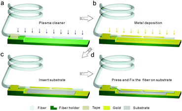
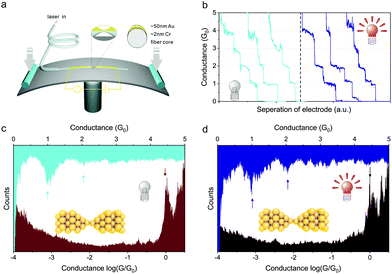
To fabricate F-MCBJ chips, we first stripped off the fiber cladding at one end of a single-mode optical fiber (∼0.5 m in length). We then placed the optical fiber wiped with alcohol cotton in an optical fiber fusion splicer (FITEL S179) and tapered it to form a constriction (∼25 μm in diameter). Since the optical fiber is relatively brittle, it can be easily broken in subsequent fabrication processes from the constriction region. Therefore, we used a piece of tape to fix the optical fiber on a step-shape holder, as shown in Fig. 1a. Following that, plasma cleaning and metal deposition processes were carried out sequentially, see Fig. 1b. Meanwhile, poly (pyromellitic dianhydride-co-4,4′-oxydianiline), amic acid (PAA) solution was spin-coated on the flexible substrate, which could be hardened by heating to form an insulation layer. The flexible substrate was prefabricated with three layers of PPA to achieve a better insulation effect, and the fourth layer of PPA solution serves as a fixed layer. After inserting the prefabricated flexible substrate between the optical fiber and the step-shape holder (Fig. 1c), we then pressed the fiber and heated it on a hot plate; the fiber will be automatically fixed on the substrate by the heating and hardening process of the PPA for 12 hours (Fig. 1d). During the whole heating process, a piece of tape is used to keep the optical fiber adhered to the metal-side facing up until it is fixed on the substrate completely. Using polyimide instead of epoxy resin to fix the tapered optical fiber core can achieve a better attenuation factor when the junction is mechanically bent and elongated using a piezo element. The fabrication and characterization of optical fiber tapering and deposition processes are presented in Fig. S1 (ESI†).To verify the reliability of the F-MCBJ, we first measured the conductance of bare metal electrodes with and without light illumination in a shielding box, as presented in Fig. 2a. We employed a home-build acquisition system to achieve automatic measurement by using the LabVIEW programming environment and the MC DT9824 USB DAQ module (see Fig. S2, ESI†). For each measurement, the electrodes were brought into contact until a conductance larger than 7 G0 was achieved, and separated until a conductance lower than 8 × 10⁻⁵G0 was achieved, where G0 = 2e2/h is the quantum of conductance. Fig. 2c and d show the conductance histograms during the electrode separation process in the absence and presence of light illumination, respectively. The typical conductance traces are presented in Fig. 2b for both cases. The individual conductance traces show characteristic plateaus at integer multiples of G0 as the electrode separation increases under dark conditions and show the same feature as well under light conditions (650 nm light passing through the fiber), as shown in Fig. 2b. Consequently, it can be found that the conductance of bare metal junctions displayed integer-multiple G0 peaks in the conductance histograms with linear coordinates, and no extra peak below 1G0 is observed with logarithmic coordinates irrespective of whether the bare metal junctions are illuminated or not.
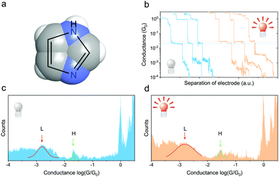
Imidazole is a planar 5-membered heterocyclic aromatic compound with two nitrogen atoms, one pyridine-like and pyrrole-like nitrogen, as depicted in Fig. 3a. By taking advantage of detailed knowledge of the transport properties of imidazole in the metal–molecule–metal junctions,29–31 we experimentally investigated the relationship between the molecular junctions and light-induced conductance enhancement. These junctions can be formed with deprotonated molecules (imidazolates), which coordinate to the metal electrodes through the nitrogen atoms.
In our experiments, the imidazole molecules were dissolved in water (10 mM) and self-assembled on the metal covered fiber for approximately 14 hours. Compared with the theoretical size of a single-imidazole junction (approximately 5 Å), the thickness of the molecular layer obtained from an ellipsometer is approximately 5.54 Å, which indicates a single-layer film. The conductance traces were recorded at a constant bias of 18 mV under ambient conditions after drying the samples in nitrogen. Similar to the bare metal junction, we observed plateaus at decreasing integer multiples of G0, indicating the mechanical thinning of gold junctions until elongating the junction into a single atom prior to rupture. We observed plateaus far below 1G0 as well, indicating that the electrodes were bridged with the target molecules. From the analysis of the conductance 1D histogram presented in Fig. 3c, two discernible peaks below 1G0 can be observed at approximately 2.1 × 10⁻²G0 and 1.6 × 10⁻³G0, labelled H and L, respectively. Because the 2D histogram may include particular information regarding the formation/evolution of junctions, we plot the 2D conductance histogram as well, see Fig. S3 (ESI†) for detailed information.
In the presence of illumination by a 650 nm light passing through the fiber, we obtain a similar molecular conductance profile, as shown in Fig. 3d. Taking a close look at the conductance histogram, two discernible peaks below 1G0 can also be found at approximately 2.9 × 10⁻²G0 and 1.6 × 10⁻³G0. Several representative traces recorded in the absence (sky blue) and presence (sand) of light illumination are shown in Fig. 3b, and the dashed lines correspond to the position of the H peak in the conductance histograms. We can draw a conclusion that the H peak shifts to a higher conductance in the presence of illumination of about 40% enhancement compared to the conductance in the dark. In contrast, the L peak mainly remains unchanged.
The conductance enhancement of single-molecule junctions upon light illumination has been reported recently by employing the STM-BJ approach.13,21,32 We want to point out that (1) the field near the tip is considerably enhanced for both the STM-BJ approach and the F-MCBJ approach, which strongly strengthen the interaction between light and single molecules; (2) the gap size can be more precisely controlled by F-MCBJ due to the pronounced attenuation factor (the ratio between the vertical movement of push rod and the horizontal separation of electrodes) originated from the three-point bending mechanism, which is critical for extreme optics.
Theoretical modelling
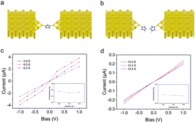
To provide a theoretical model for two peaks obtained from the F-MCBJ measurements, we have performed transport calculations by employing density functional theory (DFT) in TranSIESTA electronic transport package.33,34 We first carried out geometric optimizations of the single-imidazole junction with various gap sizes (5.8 Å, 6.0 Å and 6.2 Å) in the Gaussian 09 package.35 For each gap size, the Lanl2DZ basis was chosen, and the electrode atoms were frozen when performing the geometric optimization. The models for geometric optimizations consist of two innermost layers of Au(100) electrode units and a single imidazole bonded to the electrodes on the top sites. The deprotonated imidazole is absorbed on the gold electrodes through interactions with the lone pair on the sp2 nitrogen, as illustrated in Fig. 4a. The optimized structures for different gap sizes are shown in Fig. S4 (ESI†).We then calculated the zero-voltage transmission coefficient as a function of energy using Siesta and Gollum codes23,33 to verify the H peak in the histograms. The whole device includes three parts: two semi-infinite electrodes and the central region. Here, the unit cell of the left/right semi-infinite electrode consists of 4 layers of Au(100), 100(5 × 5 × 4) atoms in total. And the geometric structure of the central region was inherited from the result of optimization in Gaussian 09. The simulations were performed with the Perdew–Burke–Ernzerhof (PBE) functional in the generalized gradient approximation (GGA) for exchange–correlation.36 A basis set of double-zeta plus single polarization (DZP) for H, C, N and single-zeta plus single polarization (SZP) for Au was employed. The mesh cut-off value for real-space grid sampling is 230 Ry. During the self-consistent loop calculations, the convergence criterion for Hamiltonian was set to be 1.0 × 10⁻⁴ Hartree. The current of the investigated molecular devices under a finite bias voltage can be evaluated based on equilibrium theory by employing Gollum codes. Fig. 4c shows the current–voltage characteristics in the bias range of [−1.0 V, 1.0 V], and the inset illustrates the relationship between the corresponding average conductance value and the gap size. The average conductance from simulations (6.2 × 10⁻²G0 @5.8 Å, 3.2 × 10⁻²G0 @6.0 Å, and 4.2 × 10⁻²G0 @6.2 Å) is in agreement with the experiment, although slightly larger than the experimental conductance (2.1 × 10⁻²G0). The evolution of the molecular projected self-consistent Hamiltonian (MPSH) states and their energy eigenvalues of the imidazole monomer junction from HOMO−2 to LUMO+2 at 6.2 Å gap size are presented in Fig. S5 (ESI†).
Experimental and theoretical studies on the conductance of DNA junctions have been reported,37,38 in which the nitrogenous bases of the two separate polynucleotide strands are bound together with hydrogen bonds to make double-stranded DNA. Depending on the environment of the donor and acceptor atoms, the energy of a hydrogen bond can vary between 0.2 and 40 kcal mol−1, which makes them stronger than van der Waals interactions.39 Therefore, imidazole can form a strong H-bonding dimer due to the presence of both a hydrogen bond donor and a hydrogen bond acceptor. To this end, we further investigated the dimer linked by hydrogen bonds in the single-molecule junctions, and the structure is shown in Fig. 4b. After geometric optimization, the transport characteristics for different gap sizes can be observed from Fig. 4d and Fig. S4 (ESI†). The average conductance from simulations (2.9 × 10⁻³G0 @10.0 Å, 2.7 × 10⁻³G0 @10.2 Å and 2.5 × 10⁻³G0 @10.4 Å) is in agreement with the L peak in the experiments. The evolution of MPSH states and their energy eigenvalues of the imidazole dimer junction from HOMO−2 to LUMO+2 at 10.2 Å gap size are presented in Fig. S6 (ESI†).
We now turn to reveal the mechanism for the conductance enhancement, shown in Fig. 3b. One can calculate the current under an applied bias voltage in the absence of light using the Landauer formula.40
 | (1) |
![[thin space (1/6-em)]](https://www.rsc.org/images/entities/char_2009.gif) ωt can induce inelastic tunnel events when the electrons exchange energy quanta, i.e. photons, with the oscillating field, so-called photon-assisted tunneling.41 The junction transmission function under illumination can be described as42
ωt can induce inelastic tunnel events when the electrons exchange energy quanta, i.e. photons, with the oscillating field, so-called photon-assisted tunneling.41 The junction transmission function under illumination can be described as42 | (2) |
 . Higher-order Bessel function values can be neglected due to the small oscillation field compared to the photon energy. Herein, we only consider single-photon absorption during the electron transport process in the presence of illumination. Therefore, the current under illumination can be described by substituting the modified transmission function into eqn (1).
 | (3) |
 is a constant. Eqn (3) suggests that the current under illumination is proportional to the dark current with a downward shifting of the transmission function by ħω (or upward shifting of the bias window by ħω).
To calculate the current under illumination, we technically carried out the dark current calculations by shifting the reference energy down ħω (1.907 eV) in Gollum codes. Fig. 5a and b show the schematic diagram of the bias windows shifting from the original region (ice blue) to the photon absorption region (magenta) based on the zero-voltage transmission function of the imidazole monomer and dimer, respectively. The integral of the transmission function in the bias windows represent the conductance. We can observe that there is a dramatical conductance enhancement in the modified transmission function for imidazole monomer junctions, while a slight change for imidazole dimer junctions. Fig. 5c shows the current–voltage characteristics in the bias range of [−1.0 V, 1.0 V] based on the modified transmission function for imidazole monomer junctions, and the inset illustrates the relationship between the corresponding average conductance value and the gap size in the absence (black) and presence (red) of illumination. The average conductance from the modified transmission function simulations (15.2 × 10⁻²G0 @5.8 Å, 14.6 × 10⁻²G0 @6.0 Å, and 22.2 × 10⁻²G0 @6.2 Å) is approximately 310% higher than the dark conductance. Fig. 5d shows the current–voltage characteristics based on the modified transmission function for imidazole dimer junctions, and the inset illustrates the relationship between the corresponding average conductance value and the gap size in the absence (black) and presence (red) of illumination. The average conductance from the modified transmission function simulations (2.8 × 10⁻³G0 @10.0 Å, 2.9 × 10⁻³G0 @10.2 Å and 3.1 × 10⁻³G0 @10.4 Å) is only approximately 11% higher than the dark conductance. Considering the given probability  , the conductance enhancement of imidazole dimer junctions can be neglected. This can explain the obvious difference of the H peak before and after the light illumination in the experiments, while the L peak has no obvious change. Our further calculations show that this probable conductance is unlikely to originate from a pi–pi stacking dimer, see Fig. S7 (ESI†) for detailed information. Finally, we want to point out that the process of photon absorption and emission is a dynamical process, and the photon adsorption assisted tunneling might be inefficient to shift the transmission function (especially upon weak photo flux). Therefore, a more elaborated theoretical model is desired.
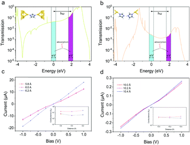 | ||
| Fig. 5 Zero-bias transmission spectrum of the imidazole monomer junction at 6.2 Å gap size (a), and of the imidazole dimer at 10.2 Å gap size (b). The bias voltage window shifts from the ice blue region to the magenta region due to photon absorption. Calculated current–voltage characteristics for the imidazole monomer (c) and imidazole dimer (d) with electron-photon coupling. The corresponding features in the dark are shown in Fig. 4c and d. Insets: Log conductance values in the absence (black) and presence (red) of photon absorption under different gap sizes. | ||
In this work, a tapered optical fiber is used as a light wave guide. This lens-free F-MCBJ, on one hand, can be used to address the electrical properties of single-molecule junctions under focused light illumination. On employing this F-MCBJ, the molecule is only exposed to the light carried by the fiber with fixed parameters (e.g., polarization, intensity), and unexpected influence (e.g., scattering from an underneath substrate) can be suppressed. On the other hand, this F-MCBJ can also be potentially employed to detect the optical signals of single molecules (e.g., photoluminescence, scattering/adsorption spectrum) due to its particular configuration: the metal coated fiber was broken into two probes, thus one can serve as an optical source channel and the other can serve as an optical collection channel. This tip-to-tip configuration, similar to double-probe aperture-type scanning near-field optical microscopy (SNOM),43 can be used to improve the efficiency of effective signal collection via near-field detection, in which the far-field background signal from electrodes/substrate can be excluded considerably.
Conclusions
In conclusion, we developed an in situ single-molecule photoconductivity integrated test system based on fiber tapering and mechanically controllable break junction technique. In experiments, we verified the stability and reliability of the system by investigating the bare metal junctions and single-imidazole junctions in the absence and presence of light illumination. We found two peaks below 1G0 in single-imidazole conductance measurements, which resulted from the formation of imidazole monomers and hydrogen bond linked dimers, respectively. The theoretical simulations by employing the DFT method agree well with the experimental results. Notably, we experimentally show that the conductance of a single-imidazole junction can be enhanced by approximately 40% upon light illumination, which is coherent with theoretically calculated results employing the single-photon absorption model. In contrast, the conductance almost remains unchanged for imidazole dimer junctions, indicating that the photon assisted tunneling strongly depends on the type of junction, i.e, the transmission function of the junction. This work provides a platform for the observation of the interaction between single molecules and fiber transmitted light, which can carry fruitful information, such as polarization, modes and orbital angular momentum.Author contributions
Z. Z., L. N. and D. X. conceived the work. Z. Z. and C. G. performed the break junction experiments and analysed the data. Z. Z. and X. Z. performed the DFT calculations and compiled the theoretical contributions.Conflicts of interest
The authors declare no competing financial interest.Acknowledgements
We acknowledge the financial support from the National Natural Science Foundation of China (91950116 and 11804170), the Natural Science Foundation of Tianjin (19JCZDJC31000 and 19JCJQJC60900).Notes and references
- D. Xiang, X. Wang, C. Jia, T. Lee and X. Guo, Chem. Rev., 2016, 116, 4318–4440 CrossRef CAS PubMed.
- C. Jia, A. Migliore, N. Xin, S. Huang, J. Wang, Q. Yang, S. Wang, H. Chen, D. Wang, B. Feng, Z. Liu, G. Zhang, D.-H. Qu, H. Tian, M. A. Ratner, H. Q. Xu, A. Nitzan and X. Guo, Science, 2016, 352, 1443–1445 CrossRef CAS PubMed.
- S. V. Aradhya and L. Venkataraman, Nat. Nanotechnol., 2013, 8, 399 CrossRef CAS PubMed.
- M. Vadai, N. Nachman, M. Ben-Zion, M. Bürkle, F. Pauly, J. C. Cuevas and Y. Selzer, J. Phys. Chem. Lett., 2013, 4, 2811–2816 CrossRef CAS.
- A. Giguère, M. Ernzerhof and D. Mayou, J. Phys. Chem. C, 2018, 122, 20083–20089 CrossRef.
- H. Song, Y. Kim, Y. H. Jang, H. Jeong, M. A. Reed and T. Lee, Nature, 2009, 462, 1039–1043 CrossRef CAS.
- C. Guo, X. Chen, S.-Y. Ding, D. Mayer, Q. Wang, Z. Zhao, L. Ni, H. Liu, T. Lee, B. Xu and D. Xiang, ACS Nano, 2018, 12, 11229–11235 CrossRef CAS PubMed.
- D. Xiang, H. Jeong, D. Kim, T. Lee, Y. Cheng, Q. Wang and D. Mayer, Nano Lett., 2013, 13, 2809–2813 CrossRef CAS.
- L. Gerhard, K. Edelmann, J. Homberg, M. Valášek, S. G. Bahoosh, M. Lukas, F. Pauly, M. Mayor and W. Wulfhekel, Nat. Commun., 2017, 8, 14672 CrossRef PubMed.
- I. Franco, C. B. George, G. C. Solomon, G. C. Schatz and M. A. Ratner, J. Am. Chem. Soc., 2011, 133, 2242–2249 CrossRef CAS PubMed.
- X. Xiao and N. Tao, J. Am. Chem. Soc., 2004, 126, 5370–5371 CrossRef CAS.
- M. Kamenetska, J. R. Widawsky, M. Dell’Angela, M. Frei and L. Venkataraman, J. Chem. Phys., 2017, 146, 092311 CrossRef.
- E. D. Fung, O. Adak, G. Lovat, D. Scarabelli and L. Venkataraman, Nano Lett., 2017, 17, 1255–1261 CrossRef CAS.
- N. Darwish, A. C. Aragonès, T. Darwish, S. Ciampi and I. Díez-Pérez, Nano Lett., 2014, 14, 7064–7070 CrossRef CAS PubMed.
- Y. Kim, T. J. Hellmuth, D. Sysoiev, F. Pauly, T. Pietsch, J. Wolf, A. Erbe, T. Huhn, U. Groth, U. E. Steiner and E. Scheer, Nano Lett., 2012, 12, 3736–3742 CrossRef CAS PubMed.
- S. Cai, W. Deng, F. Huang, L. Chen, C. Tang, W. He, S. Long, R. Li, Z. Tan, J. Liu, J. Shi, Z. Liu, Z. Xiao, D. Zhang and W. Hong, Angew. Chem., Int. Ed., 2019, 58, 3829–3833 CrossRef CAS PubMed.
- S. Kohler, J. Lehmann and P. Hänggi, Phys. Rep., 2005, 406, 379–443 CrossRef CAS.
- R. Arielly, A. Ofarim, G. Noy and Y. Selzer, Nano Lett., 2011, 11, 2968–2972 CrossRef CAS PubMed.
- M. Galperin and A. Nitzan, J. Chem. Phys., 2006, 124, 234709 CrossRef PubMed.
- M. Galperin and A. Nitzan, Phys. Chem. Chem. Phys., 2012, 14, 9421–9438 RSC.
- J. Zhou, K. Wang, B. Xu and Y. Dubi, J. Am. Chem. Soc., 2018, 140, 70–73 CrossRef CAS PubMed.
- B. Xu and N. J. Tao, Science, 2003, 301, 1221–1223 CrossRef CAS PubMed.
- J. Ferrer, C. J. Lambert, V. M. García-Suárez, D. Z. Manrique, D. Visontai, L. Oroszlany, R. Rodríguez-Ferradás, I. Grace, S. W. D. Bailey, K. Gillemot, H. Sadeghi and L. A. Algharagholy, New J. Phys., 2014, 16, 093029 CrossRef.
- D. Xiang, H. Jeong, T. Lee and D. Mayer, Adv. Mater., 2013, 25, 4845–4867 CrossRef CAS.
- C. Huang, M. Jevric, A. Borges, S. T. Olsen, J. M. Hamill, J.-T. Zheng, Y. Yang, A. Rudnev, M. Baghernejad, P. Broekmann, A. U. Petersen, T. Wandlowski, K. V. Mikkelsen, G. C. Solomon, M. B. Nielsen and W. Hong, Nat. Commun., 2017, 8, 15436 CrossRef CAS.
- M. A. Reed, C. Zhou, C. J. Muller, T. P. Burgin and J. M. Tour, Science, 1997, 278, 252–254 CrossRef CAS.
- H. Park, A. K. L. Lim, A. P. Alivisatos, J. Park and P. L. McEuen, Appl. Phys. Lett., 1999, 75, 301–303 CrossRef CAS.
- Z. Zhao, R. Liu, D. Mayer, M. Coppola, L. Sun, Y. Kim, C. Wang, L. Ni, X. Chen, M. Wang, Z. Li, T. Lee and D. Xiang, Small, 2018, 14, 1703815 CrossRef PubMed.
- C. Wu, A. Alqahtani, S. Sangtarash, A. Vezzoli, H. Sadeghi, C. M. Robertson, C. Cai, C. J. Lambert, S. J. Higgins and R. J. Nichols, Nanoscale, 2020, 12, 7914–7920 RSC.
- X. Pan, B. Lawson, A. M. Rustad and M. Kamenetska, Nano Lett., 2020, 20, 4687–4692 CrossRef CAS PubMed.
- T. Fu, S. Smith, M. Camarasa-Gómez, X. Yu, J. Xue, C. Nuckolls, F. Evers, L. Venkataraman and S. Wei, Chem. Sci., 2019, 10, 9998–10002 RSC.
- Z. Bei, Y. Huang, Y. Chen, Y. Cao and J. Li, Chem. Sci., 2020, 11, 6026–6030 RSC.
- J. M. Soler, E. Artacho, J. D. Gale, A. García, J. Junquera, P. Ordejón and D. Sánchez-Portal, J. Phys.: Condens. Matter, 2002, 14, 2745–2779 CrossRef CAS.
- K. Stokbro, J. Taylor, M. Brandbyge and P. OrdejÓN, Ann. N. Y. Acad. Sci., 2003, 1006, 212–226 CrossRef CAS PubMed.
- M. J. Frisch, G. W. Trucks, H. B. Schlegel, G. E. Scuseria, M. A. Robb, J. R. Cheeseman, G. Scalmani, V. Barone, G. A. Petersson, H. Nakatsuji, X. Li, M. Caricato, A. V. Marenich, J. Bloino, B. G. Janesko, R. Gomperts, B. Mennucci, H. P. Hratchian, J. V. Ortiz, A. F. Izmaylov, J. L. Sonnenberg, F. D. Williams, F. Lipparini, F. Egidi, J. Goings, B. Peng, A. Petrone, T. Henderson, D. Ranasinghe, V. G. Zakrzewski, J. Gao, N. Rega, G. Zheng, W. Liang, M. Hada, M. Ehara, K. Toyota, R. Fukuda, J. Hasegawa, M. Ishida, T. Nakajima, Y. Honda, O. Kitao, H. Nakai, T. Vreven, K. Throssell, J. A. Montgomery Jr., J. E. Peralta, F. Ogliaro, M. J. Bearpark, J. J. Heyd, E. N. Brothers, K. N. Kudin, V. N. Staroverov, T. A. Keith, R. Kobayashi, J. Normand, K. Raghavachari, A. P. Rendell, J. C. Burant, S. S. Iyengar, J. Tomasi, M. Cossi, J. M. Millam, M. Klene, C. Adamo, R. Cammi, J. W. Ochterski, R. L. Martin, K. Morokuma, O. Farkas, J. B. Foresman and D. J. Fox, Gaussian 09 Rev. D.01, Wallingford, CT, 2009 Search PubMed.
- J. P. Perdew, K. Burke and M. Ernzerhof, Phys. Rev. Lett., 1996, 77, 3865–3868 CrossRef CAS PubMed.
- B. Xu, P. Zhang, X. Li and N. Tao, Nano Lett., 2004, 4, 1105–1108 CrossRef CAS.
- S. Afsari, L. E. Korshoj, G. R. Abel, S. Khan, A. Chatterjee and P. Nagpal, ACS Nano, 2017, 11, 11169–11181 CrossRef CAS PubMed.
- T. Steiner, Angew. Chem., Int. Ed., 2002, 41, 48–76 CrossRef CAS.
- R. Landauer, IBM J. Res. Dev., 1957, 1, 223–231 Search PubMed.
- P. K. Tien and J. P. Gordon, Phys. Rev., 1963, 129, 647–651 CrossRef.
- G. Platero and R. Aguado, Phys. Rep., 2004, 395, 1–157 CrossRef.
- P. Bazylewski, S. Ezugwu and G. Fanchini, Appl. Sci., 2017, 7, 973 CrossRef.
Footnote |
| † Electronic supplementary information (ESI) available: Optical tapering process and additional calculation results. See DOI: 10.1039/d1nh00031d |
| This journal is © The Royal Society of Chemistry 2021 |

