
 Open Access Article
 This Open Access Article is licensed under a Creative Commons Attribution-Non Commercial 3.0 Unported Licence
Fermi level tuning in modified Bi2Te3 system for thermoelectric applications
P. Shyni and
P. P. Pradyumnan*
Department of Physics, University of Calicut, Kerala, India. E-mail: shynip1981@gmail.com; drpradyumnan@gmail.com
First published on 22nd January 2021
Abstract
The techniques of size reduction and defect engineering have attracted great interest as an effective strategy for developing new and modified thermoelectric materials with high performance. Here, we investigated the thermoelectric properties of the Bi2Te3 system modified by Fermi level tuning through the methods of nanostructuring and doping. Band structure modification and Fermi level shift contribute to the better thermoelectric performance of the material. A minimum thermal conductivity of 0.72 W K−1 was obtained at 440 K with a reduction of 50% as compared to the pristine sample. The improved transport properties along with considerably reduced thermal conductivity result in a two-fold improved figure of merit of 0.295 at 420 K for the nanostructured sample Bi0.4Sb1.6Te3 over pristine Bi2Te3.
Introduction
Nowadays, research has been focused on searching for alternative energy sources as a remedy for the energy crisis and environmental deterioration.1–3 The demand for energy is rising significantly and we still depend mainly on fossil fuels for energy generation. Tremendous energy is wasted in the form of heat, escalating global warming. Thermoelectric materials, capable of interconverting heat and electricity, can be assembled to construct a thermoelectric generator (TEG) which can be used to collect wasted heat and to convert it into useful energy, thereby improving fuel efficiency. Thermoelectric power generation offers an alternative energy source and sustainable technology. Without mechanical parts, noise and gas emission, TEGs can work for a long period without any maintenance. TEGs are utilized in deep space missions, automotive industry, gas and temperature sensors and in many other applications.4,5However, the use of TEGs is limited due to their low conversion efficiency. An efficiency of 12% is reported for Bi2Te3 based skutterudite materials, but still non-competitive with conventional machines.6 The ever-growing market of alternative energy sources demand thermoelectric materials with better conversion efficiency. The conversion efficiency of a thermoelectric material can be expressed in terms of its dimensionless figure of merit, ZT = S2σT/κ, where S, σ, κ and T represents the Seebeck coefficient, electrical conductivity, thermal conductivity and absolute temperature respectively.7 A good thermoelectric material should have high value of Seebeck coefficient for producing more voltages for a given temperature gradient, low electrical resistivity for reducing Joule's heating and low thermal conductivity to maintain the applied temperature gradient across the legs. Thermoelectric figure of merit of a material is the parameter evaluating all these interconnected properties. The main challenge in designing a superior thermoelectric material is to decouple these inter-related physical quantities via various strategies and optimize them simultaneously.
Bi2Te3 has been recognized as a benchmark thermoelectric material for near-room temperature power generation and cooling applications. It is a multi-valleyed material with a highly anisotropic isoenergy surface near the L point in the Brillouin zone. Thermoelectric devices based on bismuth telluride are widely used in the fabrication of thermal sensors, laser diodes, thermoelectric refrigeration and power generation.8–10 The large-scale production of Bi2Te3 based alloys has been limited by their relatively low efficiency. The conversion efficiency of Bi2Te3 is to be improved so that their practical applications can be boosted in wide areas of interest. The idea of using low dimensional structures to extent the value of figure of merit was proposed in early 1990's to improve the thermoelectric performance of materials, which opens up a new era in the field of thermoelectricity. Nanosized Bi2Te3 with excellent thermoelectric properties was reported by several research groups and the high performance is attributed to the reduction in grain size and thermal conductivity reduction at phonon scattering centers.11–13 The reduction in dimensions enhances (i) the density of states near the vicinity of the Fermi energy (ii) the phonon boundary scattering at interfaces and (iii) carrier mobility at a given concentration due to quantization effect. Among Bi2Te3 based alloys, n-type Bi2(Te,Se)3 and p-type (Bi,Sb)2Te3 alloys are of great interest for room temperature applications because of their potential for improving the conversion efficiency by structural and compositional modifications.14,15 The electrical transport properties can be optimized by modifying the carrier concentration and energy band structure of material and thermal conductivity reduction can be achieved by nanostructuring and defect engineering. Lipeng Hu et al. reported the role of point defect engineering in tuning thermoelectric properties.16 Thermal conductivity reduction through augmenting lattice scattering by ionized impurity scattering and improved thermoelectric performance is reported for the combination of Bi0.4Sb1.6Te3.17,18
In this study, Bi2Te3 was synthesized via solid state reaction route, nanostructured via ball milling and compacted by hot pressing method. The effect of Fermi level modification, through grain size reduction and point defect engineering, on the thermoelectric properties of the as synthesized samples was studied in the temperature range of 300–480 K.
Experimental procedure
Elemental Bi (99%) and Te (99.99%) powder, obtained from Sigma Aldrich, were weighed according to the stoichiometric composition and the powder mixture was loaded into carbon coated quartz ampoule, evacuated and sealed under vacuum at 10−3 pascal. The ingot obtained after pre heating was hand ground using agate mortar and pestle and the powder was mechanically pressed to form a pellet. This pellet was again charged into a carbon coated quartz tube, evacuated and sealed at 10−5 Pa, heated in a furnace at 823 K for 18 hours, furnace cooled to room temperature, ground in agate mortar and pestle to form Bi2Te3 powder. This manually ground powder was subjected to ball milling for 4 hours at milling speed of 200 rpm to obtain nanopowder of Bi2Te3 (sample BT).The as prepared BT nanopowder was again ball milled for 1 hour at a milling speed of 400 rpm to obtain nanopowder of Bi2Te3 with reduced grain size (BTN).
The synthesis of Bi0.4Sb1.6Te3 sample through solid state reaction route was reported in our previous work.19 The as synthesized powder was subjected to ball milling for 4 hours at milling speed of 200 rpm and then again ball milled at 400 rpm for 1 hour to obtain nanopowder of Bi0.4Sb1.6Te3 (sample BSbTN).
The crystal phase of the samples was confirmed by analyzing X-ray diffraction pattern obtained from Rigaku Miniflex X-ray diffractometer using Cu Kα radiation (λ = 1.54 Å) before and after hot pressing. The micro structural morphology was observed by field emission scanning electron microscopy (ZEISS-FESEM) and energy dispersive spectroscope attached with SEM respectively. Archimedes method was used to determine the density of the samples and verification is done by volumetric method. The Hall coefficient RH, carrier concentration n and mobility of the carrier μ were measured using van der Pauw method with magnetic field strength of 0.55 T. Thermoelectric parameters such as Seebeck coefficient and electrical resistivity of the samples were determined by using Ulvac-Riko ZEM-3 (M8) equipment under low pressure helium environment with temperature ranging from 300 K to 480 K. The thermal conductivity of the rectangular bar shaped (10 × 3 × 1 mm3) sample was measured by steady state method. The temperature gradient was maintained in the sample and the temperature was recorded using the standard copper–constantan thermocouple.
Results and discussion
Morphological and structural analysis
XRD pattern of the samples BT, BTN and BSbTN are shown in Fig. 1. The diffraction peaks of the samples BT and BTN can be indexed to JCPDS card no. 00-015-0863 indicating the formation of single phase and polycrystalline Bi2Te3 with rhombohedral structure. All the peaks of BSbTN be indexed to # JCPDS 01-72-1836 which indicates the formation of single phase and polycrystalline Bi0.4Sb1.6Te3 having hexagonal structure with lattice parameters a = 4.248 Å and c = 30.28 Å. The average crystallite size was calculated by using Debye–Scherrer equation, d = kλ/β![[thin space (1/6-em)]](https://www.rsc.org/images/entities/char_2009.gif) cosθ, where k = 0.93, λ is Cu-Kα wavelength (λ = 1.54 Å), θ is the Bragg's angle and β is the full width at half maximum of the peak. The average crystallite size for the planes [015], [1010] and [110] was calculated to be 41.2 nm, 32.5 nm and 24.8 nm for the samples BT, BTN and BSbTN respectively. It can be seen that the average crystallite size is reduced by 20% for the samples BTN and 40% for the sample BSbTN compared to pristine BT.
cosθ, where k = 0.93, λ is Cu-Kα wavelength (λ = 1.54 Å), θ is the Bragg's angle and β is the full width at half maximum of the peak. The average crystallite size for the planes [015], [1010] and [110] was calculated to be 41.2 nm, 32.5 nm and 24.8 nm for the samples BT, BTN and BSbTN respectively. It can be seen that the average crystallite size is reduced by 20% for the samples BTN and 40% for the sample BSbTN compared to pristine BT.
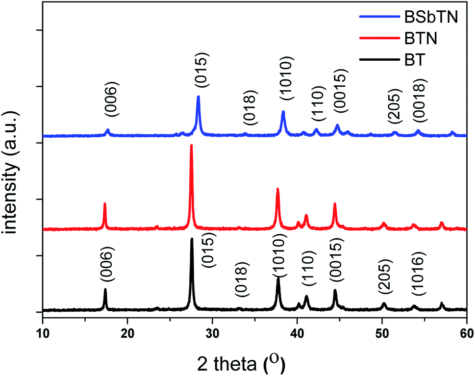 | ||
| Fig. 1 XRD pattern of the samples BT, BTN and BSbTN. | ||
The morphological analysis of the samples was carried out and the FESEM images depicted in Fig. 2(a–c) shows agglomerated grains of the samples BT, BTN and BSbTN respectively with size ranging from 20 nm to 1 μm. The layered structure of Bi2Te3 and Bi0.4Sb1.6Te3 is visible in the figure.
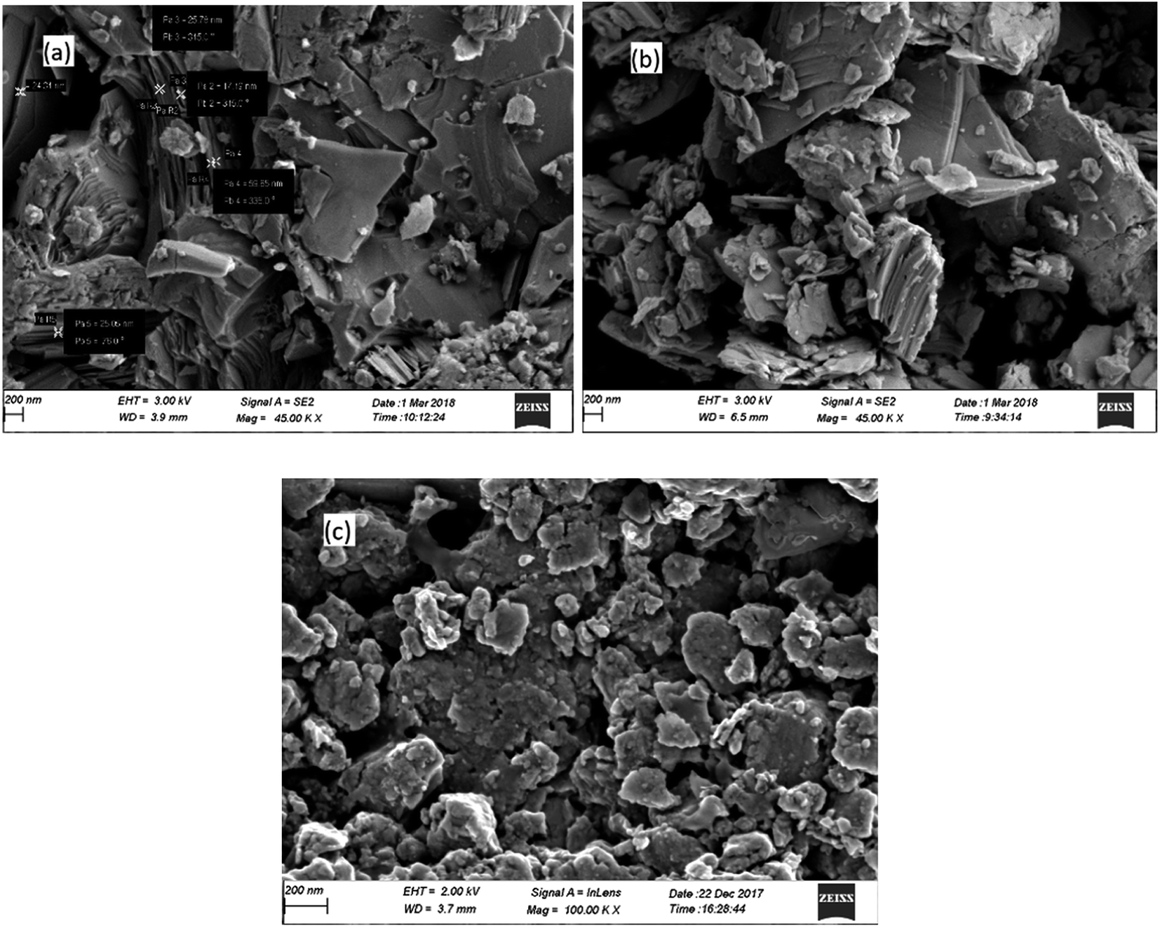 | ||
| Fig. 2 FESEM images of the samples (a) BT, (b) BTN and (c) BSbTN. | ||
Archimedes method was used to determine the density of the samples and verification was done by volumetric method. The density values obtained were presented in Table 1. All the samples were found to be compacted well.
| Sample name | Actual density (g cm−3) | Relative density (%) |
|---|---|---|
| BT | 7.66 | 99.5 |
| BTN | 7.08 | 91.9 |
| BSbTN | 6.31 | 93.1 |
Electrical transport property studies
The variation of electrical conductivity of the samples BT, BTN and BSbTN are depicted in Fig. 5(a). The electrical conductivity of all the samples falls off with increase in temperature for the entire temperature range, indicating degenerate semiconducting behavior of the material. The sample BTN shows escalated electrical conductivity and the sample BSbTN shows declined electrical conductivity compared to that of the pristine sample. The sample BTN shows an electrical conductivity around three-fold greater than that of pristine sample at room temperature.The electrical conductivity of a material is related to carrier concentration (n) and mobility of charge carrier (μ) through the relation, σ = neμ, where e is the electronic charge.
The Hall coefficient RH, n, μ and effective mass m* were measured using van der Pauw method with magnetic field strength of 0.55 T and the obtained values are recorded in Table 2.
| Sample name | n (1019 cm−3) | μ (cm2 V−1 s−1) | m* (me) |
|---|---|---|---|
| BT | 2.49 | 61.42 | 0.548 |
| BTN | 5.93 | 113.98 | 0.534 |
| BSbTN | 6.49 | 11.19 | 0.305 |
From the table, it can be seen that n is greater for the samples BTN and BSbTN than BT. The Hall mobility is found to be decreased for BSbTN sample, presumably due to scattering of carriers by point defects and carrier–carrier scattering due to high carrier density.
The hike in carrier concentration of BTN may be attributed to a donor-like effect induced due to the mechanical deformation by excessive ball milling and subsequent hot pressing.20 Deformation induces non-basal slip and creates an average of 3Te to 2Bi vacancy–interstitial pairs.21 When large number of Bi vacancies are created, the Bi atoms occupying the Te sites diffuses back to their original sublattices producing Te vacancies.20

 and
and  represents the Bi and Te vacancies generated during the ball milling deformation process,
  is the antisite defect formed during crystal growth and e′ is an excess electron. The Te layers are connected by the weak van der Waals bonding and due to mechanical deformation, cleavage slip occurs between Te layers generating Te vacancies. Due to the small electronegativity difference between Bi and Te, Bi atoms occupying Te vacancies results in an antisite defect
  and a vacancy VBi.22,23 The available additional electrons create donor-like effect which accounts for the large value of n for the nanostructured sample BTN. The impact level of donor-like effect is determined by the concentration of antisite defects.
In the sample BSbTN, n increases with respect to the sample BT as a result of the higher antisite defects due to larger electro negativity difference between Bi and Te than that between Sb and Te.24,25 The formation of antisite defects in Bi0.4Sb1.6Te3 crystals was caused by the low polarity of Bi–Te and Sb–Te bonds. Whenever the difference in electro negativity value of the component atoms decreases, the ability to form antisite defects increases (χSb = 1.9, χBi = 1.8 and χTe = 2.1). The Bi and Sb atoms occupying the Te sites account for the creation of holes and p-type semiconducting behavior of the material.26 It was already reported that in BixSb1−xTe3 crystals the hole concentration increases with increase in concentration of Sb.27,28 In Bi0.4Sb1.6Te3 structure, inherent point defects occur during growth of crystal from the melt. Here, antisite defects refers to Bi or Sb atoms occupying Te(1) sites  , Bi or Sb atoms occupying Te(2) sites
  and Te atoms occupying Bi or Sb sites (TeBi(Sb)). The formation energies of these antistructure defects were reported as 0.47, 0.76 and 0.94 eV respectively by T. Thonhauser et al.29
For the sample BTN, the higher value of n and μ account for the shoot up in its electrical conductivity. The diminished mobility of charge carriers conceals the hike in carrier concentration in the sample BSbTN, thus reduces its electrical conductivity.
The variation in Seebeck coefficient of the samples with temperature are plotted in Fig. 5(b). For the samples BT and BTN, Seebeck coefficients are negative showing that the samples are n-type semiconductors. Seebeck coefficient is positive for the sample BSbTN showing the p-type semiconducting nature of the sample. With increase in temperature, Seebeck coefficient initially increases, reaches a maximum and then decreases. Bipolar effects account for the diminishing of Seebeck coefficient at higher temperatures.30 Here, minority carriers are thermally excited at sufficiently high temperatures. Seebeck coefficient for electrons and holes are opposite in nature, hence its value decreases.
The magnitude of an individual gain in S scales roughly with the distance from Fermi energy (EF) in units of energy. Fritzsche proposed a model depicting the correlation connecting Seebeck coefficient to the energy difference between the conduction band and Fermi level when the density of states edge allows carrier motion only in the conduction band or in the valence band.31 For the n and p type semiconductors,
The terms Ac and Av accounts for the distribution of carriers beyond the conduction band Ec and below the valence band Ev respectively.

A graph is plotted with 1/T on the x-axis and −S along the y axis for n type BT and BTN samples, as shown in Fig. 3(a and b). Slope of the graph gives value of Ec − EF.32 Slope of the graph plotted with 1/T along x-axis and S along y-axis for p type BSbTN sample gives the value of EF − Ev, as estimated from Fig. 3(c). The obtained values are listed in Table 3.
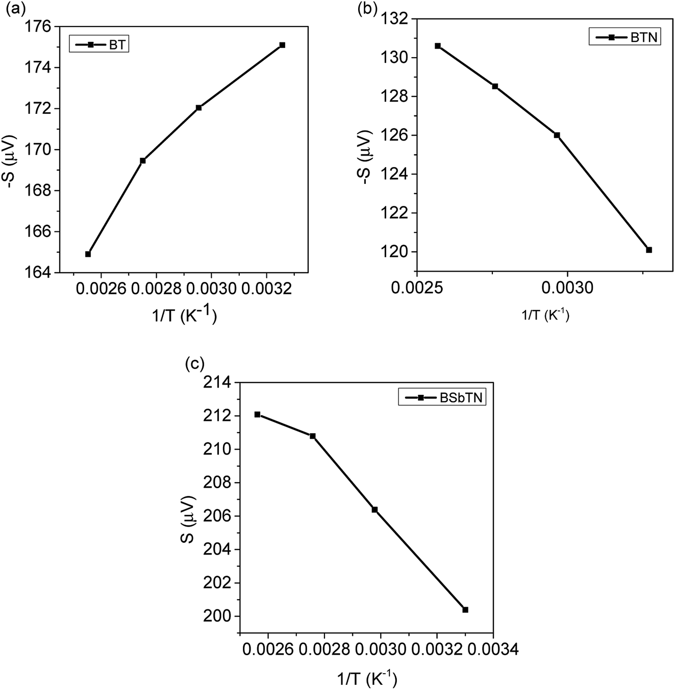 | ||
| Fig. 3 Variation of S with 1/T for the samples (a) BT, (b) BTN and (c) BSbTN. | ||
| Sample | Ec − EF (eV) | EF − Ev (eV) |
|---|---|---|
| BT | 0.011 ± 0.003 | — |
| BTN | −0.015 ± 0.001 | — |
| BSbTN | — | −0.016 ± 0.002 |
The obtained results reveal that the derived Fermi level, as measured from the conduction band edge, is positive for the sample BT showing that the Fermi level resides inside the band gap. The lower electrical conductivity of the sample BT also implies that the Fermi level is located inside the band gap. The negative value of (Ec − EF) obtained for the sample BTN shows that the Fermi level shifts above the conduction band edge and the material becomes degenerate. Electrical conductivity of the sample is enhanced, as expected. (EF − Ev) is positive for the sample BSbTN informing that the Fermi level shifts below the valence band. Here, Sb acts as an acceptor and down shift the Fermi level towards the valence band. The n to p type transition on addition of Sb also implies the Fermi level tuning from bottom of conduction band edge to top of valence band edge.
For a degenerate semiconductor, Seebeck coefficient measures the asymmetry in the electronic structure and scattering rates near Fermi energy and is connected to carrier concentration (n) and effective mass of charge carrier (m*) through Mott's relation,
Widening of band gap
The UV-visible spectroscopy studies were conducted to determine the optical band gap of the material. The fundamental optical band gap energy was calculated by using the Tauc-plot relation,| (hνF(R))2 = A(hν − Eg) |
The absolute reflectance value, R is obtained from UV-visible diffuse reflectance spectroscopy. The band gap energy of the samples BT, BTN and BSbTN were found out by extrapolating the linear part of (F(R)hν)2 to the energy axis, i.e., by extrapolating the absorption edge to zero absorption, as shown in Fig. 4(a–c). The obtained values of band gap energy were listed in Table 4.
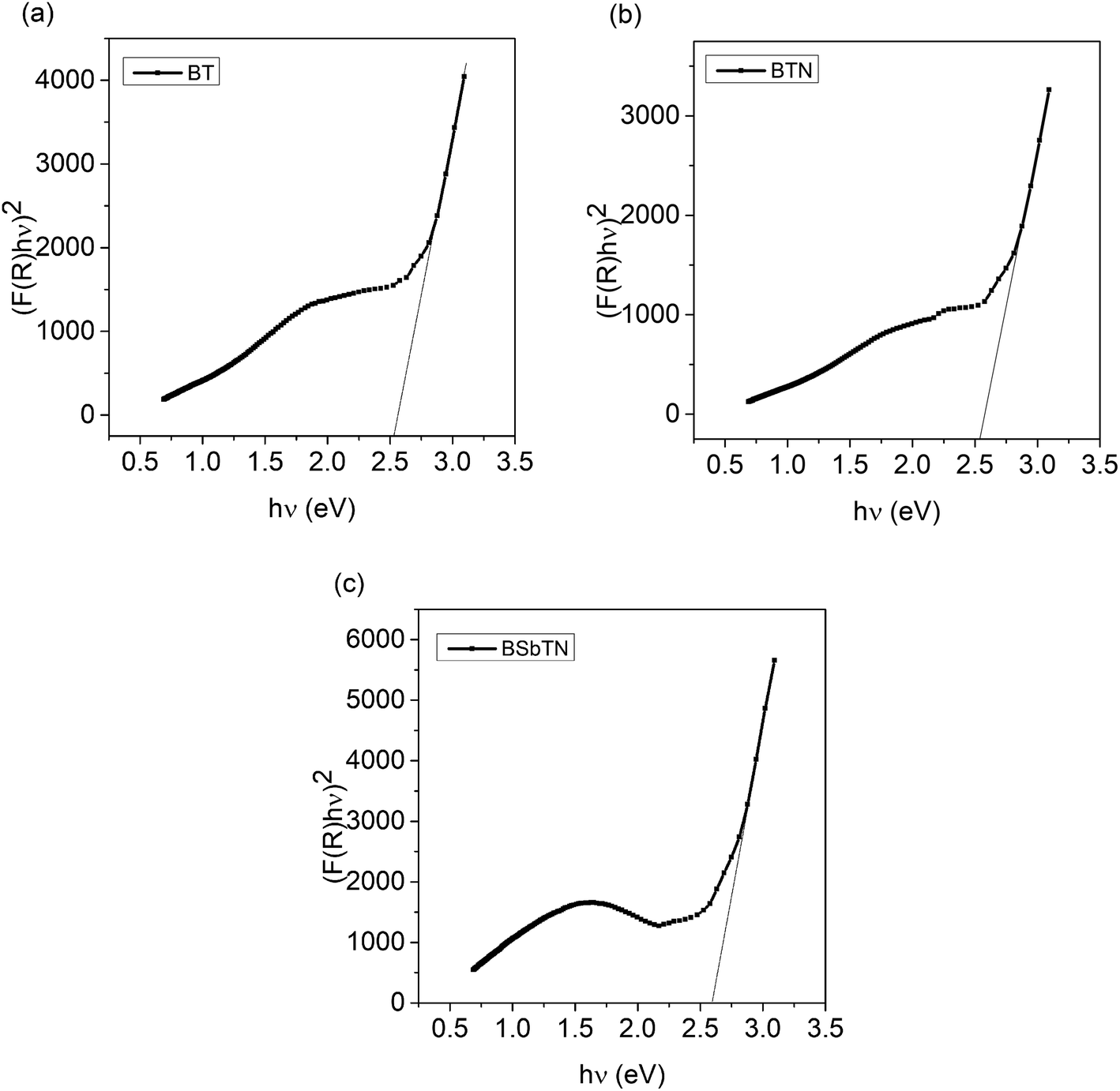 | ||
| Fig. 4 Modified Kubelka–Munk function versus hν graph of the samples (a) BT, (b) BTN and (c) BSbTN. | ||
| Sample code | Eg (eV) |
|---|---|
| BT | 2.528 ± 0.002 |
| BTN | 2.534 ± 0.001 |
| BSbTN | 2.591 ± 0.004 |
It is clear that, nanostructuring widens the band gap of Bi2Te3 by an amount of 0.014 eV for the sample BTN and the combined effect of nanostructuring and defect engineering widens the energy gap by an amount of 0.063 eV. Increment in band gap energy can be ascertained due to the apparent shift in Fermi level defined as Burstein–Moss shift.35
The variations in electrical conductivity and Seebeck coefficient with temperature reflects in the value of power factor (S2σ) as shown in Fig. 5(c). Power factor value of the sample BTN is higher and BSbTN is lower compared to that of the BT for the entire temperature range indicating that nanostructuring alone is beneficial for improving the power factor while doping with Sb results in diminished power factor. A maximum power factor value of 1.18 W mK−2 is obtained for the sample BTN at a temperature of 340 K.
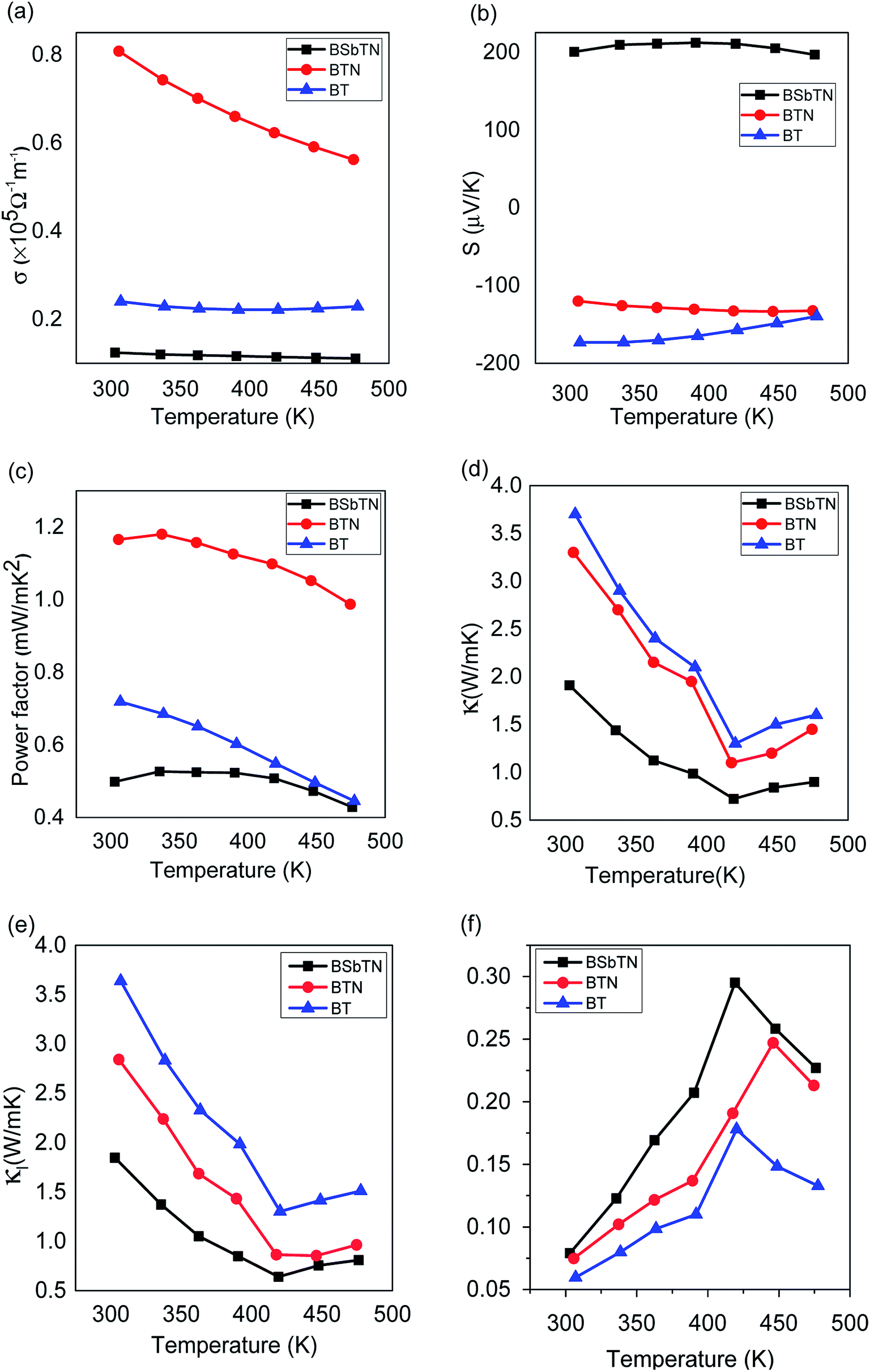 | ||
| Fig. 5 Variation of thermoelectric properties of the samples BT, BTN and BSbTN (a) electrical conductivity (b) seebeck coefficient (c) power factor (d) total thermal conductivity (e) lattice thermal conductivity and (f) figure of merit. | ||
Thermal conductivity measurements
The change in total thermal conductivity and lattice thermal conductivity of the samples BT, BTN and BSbTN with temperature were plotted in Fig. 5(d and e) respectively. The total thermal conductivity (κ) of a material is the sum of electronic, phononic and bipolar contributions.| κ = κe + κl + κb |
Weidemann–Franz law defines electronic thermal conductivity in terms of electrical conductivity as,34
| κe = L0σT |
| L0 = 1.5 + exp[−|S|/116] |
As seen in Fig. 5(d and e), the samples show similar trend in variation of κ and κl with temperature. κ initially decreases, reaches a minimum and then starts to increase. The further increase in κ at high temperature is due to onset of bipolar conduction. κ and κl values of BTN and BSbTN are lower than that of BT showing that the technique of nanostructuring and defect engineering were effective in reducing thermal conductivity of Bi2Te3. Comparing the values of κ and κl shows that the reduction in κ mainly comes from reduced κl due to enhanced scattering of phonons. It was reported that phonons with short, intermediate and long wavelengths can be scattered by structures with comparable sizes.37 In nanostructured BTN sample, phonons with intermediate wavelengths can be scattered by increased grain boundaries resulting in reduced thermal conductivity. The enhanced electrical conductivity and reduced thermal conductivity of BTN implies that phononic transport is more affected than electrons. In the sample BSbTN, phonons with short and intermediated wavelengths can be scattered by increased grain boundaries and point defects created by the substitutional Sb atoms leading to further diminished thermal conductivity.38 Both nanostructuring and defect engineering contribute to reduction in thermal conductivity and minimum κ of 0.72 W mK−1 at 420 K is obtained for the sample BSbTN, reduced by a factor of 2 compared to the sample BT.
Figure of merit
Fig. 5(f) presents the variation of ZT with temperature. It is evident that ZT value is substantially increased for the samples BTN and BSbTN compared to that of the sample BT. A peak ZT value of 0.295 is obtained at 420 K for the sample BSbTN which is two-fold greater than that of the pristine sample. The better performance of BSbTN can be attributed to the reduction in thermal conductivity due to intensified phonon scattering at the increased boundaries offered by grain size reduction and defect engineering.Conclusions
In this study, Bi2Te3 is synthesized through solid state reaction route and variation in thermoelectric properties induced via techniques of nanostructuring and defect engineering are studied. The donor-like effect induced by the mechanical deformation is found to modify the Fermi level and hence the carrier concentration, leading to better electrical properties. Thermal conductivity reduction is achieved via nanostructuring and probing antisite defects by incorporating dopant. Tuned Fermi level due to impurity addition and enhanced phonon scattering at increased boundaries of nanograins effectively change the thermoelectric figure of merit of the sample. A minimum thermal conductivity of 0.72 W mK−1 at 420 K is obtained for the sample BSbTN, reduced by a factor of 2 and a peak ZT value of 0.295 is obtained at 420 K which is two-fold greater than that of the pristine sample.Conflicts of interest
There are no conflicts of interest to declare.Acknowledgements
The authors wish to thank UGC-SAP and FIST 2 (SR/FIST/PS1-159/2010) (DST, Government of India) for the research facilities in the Department of Physics, University of Calicut. The Central Sophisticated Instrumentation Facility (CSIF), University of Calicut, provided the characterization facilities for the research work. P. P. Pradyumnan is thankful to DST SERB (Govt. of India) for a major research project (SB/EMEQ-002/20013). Shyni P. is thankful to UGC, Govt. of India for the award of Teacher Fellowship under XIIth plan of UGC SWRO's Faculty Development Programme (FIP/12th Plan/KLCA064 TF 05).References
- T. Zhu, Y. Liu, C. Fu, J. P. Heremans, J. G. Snyder and X. Zhao, Adv. Mater., 2017, 29, 1605884 CrossRef.
- C. Gayner and K. K. Kar, Prog. Mater. Sci., 2016, 83, 330 CrossRef CAS.
- G. Han, Z.-G. Chen, J. Drennan and J. Zou, Small, 2014, 10, 2747 CrossRef CAS.
- G. J. Snyder and E. S. Toberer, Nat. Mater., 2008, 7, 105–114 CrossRef CAS.
- E. Abbe, T. Schmiel and M. Tajmar, Energies, 2016, 9, 541 CrossRef.
- Q. Zhang, J. Liao, Y. Tang, M. Gu, C. Ming, P. Qiu, S. Bai, X. Shi, C. Uher and L. Chen, Energy Environ. Sci., 2017, 10, 956 RSC.
- Y. G. Deng and J. Liu, J. Renewable Sustainable Energy, 2009, 1, 052701 CrossRef.
- H. Scherrer and S. Scherrer, in Thermoelectric Handbook, ed. D. M. Rowe, CRC, New York, 2006, p. 27 Search PubMed.
- J. R. Drabble and C. H. L. Goodman, J. Phys. Chem. Solids, 1958, 5, 142–144 CrossRef CAS.
- S. Nakajima, J. Phys. Chem. Solids, 1963, 24(3), 479–485 CrossRef CAS.
- R. Venkatasubramanian, E. Siivola, T. Colpitts and B. O'Quinn, Nature, 2001, 413, 597–602 CrossRef CAS.
- L. D. Hicks and M. S. Dresselhaus, Phys. Rev. B: Condens. Matter Mater. Phys., 1993, 47, 12727 CrossRef CAS.
- B. Poudel, H. Qing, Y. Ma, Y. Lan, M. Austin, B. Yu, X. Yan, D. Wang, A. Muto, D. Vashaee, X. Chen, J. Liu, M. S. Dresselhaus, G. Chen and Z. Ren, Science, 2008, 320, 634 CrossRef CAS.
- M. Takashiri, J. Appl. Phys., 2008, 104, 084302 CrossRef.
- Z. Yan-fei, X.-y. Lin and B. Sheng-qiang, J. Cryst. Growth, 2010, 312, 775–780 CrossRef.
- L. Hu, T. Zhu, X. Liu and X. Zhao, Adv. Funct. Mater., 2014, 24(33), 5211–5218 CrossRef CAS.
- H. C. Kim, T. S. Oh and D. B. Hyun, J. Phys. Chem. Solids, 2000, 61, 743–749, DOI:10.1016/S0022-3697(99)00269-3.
- H. J. Goldsmid, J. Thermoelectr., 2006, 4, 3 Search PubMed.
- P. Shyni, P. P. Pradyumnan, P. Rajasekar, A. M. Narayanan and A. M. Umarji, J. Alloys Compd., 2020, 853, 156872, DOI:10.1016/j.jallcom.2020.156872.
- J. Navratil, Z. Stary and T. Plechacek, Mater. Res. Bull., 1996, 31, 1559 CrossRef CAS.
- R. Ionescu, J. Jaklovszky, N. Nistor and A. Chiculita, Phys. Status Solidi A, 1975, 27, 27 CrossRef CAS.
- H. C. Kim, T. S. Oh and D. B. Hyun, J. Phys. Chem. Solids, 2000, 61, 743 CrossRef CAS.
- L. D. Zhao, B. P. Zhang, J. F. Li, H. L. Zhang and W. S. Liu, Solid State Sci., 2008, 10, 651–658 CrossRef CAS.
- J. Horak, K. Cermak and L. Koudelka, J. Phys. Chem. Solids, 1986, 47, 805 CrossRef CAS.
- Z. Stray, J. Horak and M. Strordeur, J. Phys. Chem. Solids, 1988, 49, 29–34 CrossRef.
- Y. Pan, T. R. Wei, C. F. Wu and J. F. Li, J. Mater. Chem. C, 2015, 3(40), 10583–10589 RSC.
- R. F. Brebrick, J. Phys. Chem. Solids, 1969, 30, 719 CrossRef CAS.
- J. Jianga, L. Chena, S. Baia, Y. Qin and Q. Wang, J. Cryst. Growth, 2005, 277, 258–263 CrossRef.
- T. Thonhauser, G. S. Jeon, G. D. Mahan and J. O. Sofo, Phys. Rev. B: Condens. Matter Mater. Phys., 2003, 68, 205207 CrossRef.
- Y. Yuan, L. Zhang, J. Xing, M. Iqbal Bakti Utama, X. Lu, K. Du, Y. Li, X. Hu, S. Wang, G. Aziz, R. Dunin-Borkowski, J. Arbiold and Q. Xiong, Nanoscale, 2015, 7, 12343–12350 RSC.
- F. H. Fritzsche, Solid State Commun., 1971, 9, 1813e1815 CrossRef.
- A. Paulson, N. A. Muhammed saber and P. P. Pradyumnan, J. Alloys Compd., 2019, 786, 581e587 CrossRef.
- J. R. Sootsman, D. Y. Chung and M. G. Kanatzidis, Angew. Chem., Int. Ed., 2009, 48(46), 8616–8639 CrossRef CAS.
- A. Paulson, N. A. M. Sabeer and P. P. Pradyumnan, J. Alloys Compd., 2019, 786, 581–587 CrossRef CAS.
- N. R. Yogamalar and A. Chandra Bose, Appl. Phys. A: Mater. Sci. Process., 2011, 103, 33–42, DOI:10.1007/s00339-011-6304-5.
- H.-S. Kim, Z. M. Gibbs, Y. Tang, H. Wang and G. Jeffrey Snyder, APL Mater., 2015, 3, 041506 CrossRef.
- E. S. Toberer, A. Zevalkink and G. J. Snyder, J. Mater. Chem., 2011, 21, 15843 RSC.
- J. Callaway and H. C. von Baeyer, Phys. Rev., 1960, 120, 1149 CrossRef CAS.
| This journal is © The Royal Society of Chemistry 2021 |