
 Open Access Article
 This Open Access Article is licensed under a Creative Commons Attribution-Non Commercial 3.0 Unported Licence
The origins of charge separation in anisotropic facet photocatalysts investigated through first-principles calculations†
Shun-Chiao Chana,
Yu-Lin Chenga,
Bor Kae Chang *b and
Che-Wun Hong*a
*b and
Che-Wun Hong*a
aDepartment of Power Mechanical Engineering, National Tsing Hua University, Hsinchu City 300, Taiwan. E-mail: cwhong@pme.nthu.edu.tw
bDepartment of Chemical & Materials Engineering, National Central University, Taoyuan City 320, Taiwan. E-mail: BKChang@ncu.edu.tw
First published on 21st May 2021
Abstract
It was recently discovered that the oxygen evolution reaction (OER) and hydrogen evolution reaction (HER) can be completed on the {110} and {001} facets, respectively, of a 18-facet SrTiO3 mono-crystal. The effective charge separation is attributed to the facet junction at the interface between two arbitrary anisotropic crystal planes. Theoretical estimation of the built-in potential at the facet junction can greatly improve understanding of the mechanism. This work employs density functional theory (DFT) calculations to investigate such potential at the (110)/(100) facet junction in SrTiO3 crystals. The formation of the facet junction is verified by a calculated work function difference between the (110) and (100) planes, which form p-type and n-type segments of the junction, respectively. The built-in potential is estimated at about 2.9 V. As a result, with the ultra high built-in potential, electrons and holes can effectively transfer to different anisotropic planes to complete both photo-oxidative and photo-reductive reactions.
1. Introduction
Photoelectrochemistry has great potential for storing solar energy. Sunlight is absorbed by a photocatalyst to produce fuels such as oxygen and hydrogen through the oxygen evolution reaction (OER) and hydrogen evolution reaction (HER).1 The process is clean and does not need external electrical energy input, but so far, the efficiency of photoelectrochemical reactions is still very low due to low efficiency of charge separation. The photogenerated electrons and holes recombine too easily to reach active sites in the photoelectrochemical reaction, even if they have sufficient Gibbs free energy for water splitting.To enhance the charge separation efficiency, previous strategies include: (1) combining the photocatalyst with a cocatalyst to form a p–n heterojunction and introduce a built-in potential on the photocatalyst surface to promote charge separation during photocatalysis.2–16 For instance, Afshar et al. put p-type tetrahexahedron-SrTiO3 cocatalyst on n-type TiO2 to form a heterojunction to improve the efficiency of the photocatalytic reaction.17 (2) Introducing different types of defects in photocatalyst crystals to control the distribution of surface photogenerated charges and resulting charge separation.18–30 Defect engineering exploits the interesting fact that the properties of TiO2 are closely related to defect disorder in structure or composition, first proposed by Bak et al.31
For strategy (1), however, heterojunctions will gradually encounter morphological degradation, interface degradation, and photo-oxidation in time, resulting in the decrease of separation efficiency.32,33 For strategy (2), the size and location of defects are the most important factors in defect engineering.18,19 However, systematic investigations into the identity and distribution of defects before and after photocatalytic reactions have not been comprehensively performed for understanding the role of vacancies. Moreover, the stability of defects under light illumination and after photocatalytic reactions is still a question because the concentration of defects will gradually reduce after every cycle.18
Recently, it was reported that semiconductors with characteristic anisotropic facets, such as TiO2 and BiVO4, can effectively separate photogenerated electrons and holes into different facets.34–38 The phenomenon results in selective reductive or oxidative reactivity on different crystal facets. Later, it was experimentally verified that built-in potential exists at the interface between adjacent anisotropic facets of BiVO4.39 Moreover, Mu et al. even successfully used “nanocrystal morphology tailoring” strategy to transform an isotropic 6-facet SrTiO3 photocatalyst into an anisotropic 18-facet SrTiO3 crystal and improved the electron/hole separation to a great extent.40 They found that OER and HER will occur on different crystal facets after forming an anisotropic-facet SrTiO3. Therefore, the new concepts of “facet engineering” and “facet junction” were introduced.41–46 Facet engineering not only effectively avoids the recombination of electron holes, but also reduces the need to find different semiconductors to form a heterojunction. Hence, it is the most promising way to enhance photocatalytic ability.
Theoretical estimation of the built-in potential in such an anisotropic-facet photocatalyst is still lacking and cannot provide details of the mechanism. In this work, to challenge this issue, SrTiO3 is chosen as the system of interest due to its easily calculated cubic unit cell. Density functional theory (DFT) calculations have been employed to elucidate the mechanism of charge separation and calculate the built-in potential at the facet junction between the anisotropic facets in SrTiO3. Although band offsets have been calculated for a facet junction demonstrated with TiO2,63 built-in potential calculations have not been attempted on such materials. This work is the first instance of estimating the value of built-in potential at a facet junction and not just the band offsets, demonstrated with SrTiO3, and verifies that the built-in potential is the driving force for charge separation for the facet junction.
2. Computational method
2.1 Details of the DFT simulations
All the DFT calculations were performed using the CASTEP code, which uses plane waves basis sets.47,48 The generalized gradient approximation (GGA) with the Perdew–Burke–Ernzerhof (PBE) method is utilized as the exchange–correlation functional.49 The GGA+U approach is adopted to describe the correlation effects in transition metal oxide semiconductors.50 Typically, the on-site +U correction is only applied on the d and f orbitals in transition metals. However, it has been found that in certain cases the band gap is still underestimated compared with the experimental result even with high U values. To obtain the ideal band-structure, in addition to the d orbitals in transition metals (Ud), a few theoretical studies of the +U effect on p orbitals (Up) in oxygen have been discussed and has been shown to be crucial in oxides.51–55 Therefore, in this work, the GGA+Up+Ud method is used to best describe the localized transition and generate the most reliable result of band gap of SrTiO3, with the Up (4.20 eV) on O 2p and Ud (5.95 eV) on Ti 3d. On-the-fly generated (OTFG) ultrasoft pseudopotentials are employed to describe the interactions of ionic core and valance electrons.56 Also, Koelling–Harmon relativistic treatment is used for spin-polarised calculations.57 The density mixing electronic minimization algorithm is chosen for variable occupancy calculations.58 A 550 eV cut-off energy and 6 × 6 × 6 k-point Monkhorst–Pack grid have been used.59 Convergence criteria of 0.03 eV Å−1 maximum force, 0.05 GPa maximum stress, 10−3 Å maximum atomic displacement, and self-consistent field (SCF) tolerance of 10−6 eV per atom have been used in all the calculations.2.2 Average potential method
The theoretical model for estimating the conduction band offset (CBO) and the valence band offset (VBO) at a non-polar semiconductor–semiconductor interface was described by Van de Walle.60,61 Combined with DFT or hybrid DFT calculations, this model has been successfully verified for various heterojunction materials and is the most widely used one. For instance, it was combined with hybrid DFT to calculate the band offsets for SrTiO3/TiO2 (anatase) heterojunction by Liberto et al.62 Furthermore, it has been employed to study the band offsets at the (001)/(101) facet junction in anatase TiO2.63 In this work, GGA+U was employed, as it is one of the most reliable and cost-effective method for electronic band correction, allowing for calculation of larger facet models. To estimate a band offset of a non-polar heterojunction, the electrostatic potential V(x,y,z) throughout the simulated structure should be averaged with respect to the area of a unit cell S perpendicular to the direction of the extended superlattice. It was set to the xy-plane in this work. Therefore, the planar average electrostatic potential (PAEP) Ṽ(z) can be expressed as eqn (1) proposed by Van de Walle and Martin.61
 | (1) |
![[V with combining macron]](https://www.rsc.org/images/entities/i_char_0056_0304.gif) is the average of Ṽ(z) over one period with the period length p:
is the average of Ṽ(z) over one period with the period length p:
 | (2) |
Finally, the CBO and VBO of a junction A/B can be determined by eqn (3). The first two terms describe the band discontinuity across the interface between materials A and B lattice segments, and the last term is the band lineup at the interface.
|
BOC/V = [EC/V]A − [EC/V]B + Δ
| (3) |
|
Δ = [A − B]A/B
| (4) |
of A and B segments respectively. The band lineup Δ, which accounts for the built-in potential, is described as the difference of MAEP between materials A and B after the junction is formed.
3. Results and discussion
The structure model for cubic SrTiO3 is from experimental data recorded in the inorganic crystal structure database (ICSD: 23076).64 In this work, the final equilibrium structure, shown in Fig. 1(a), with lattice constants of a = b = c = 3.905 Å, β = 90.00° are consistent with the experimental results found by Nelmes et al.64 For comparison, other experimental and theoretical lattice constants along with the band gap are listed in Table 1.54,55,65,66 The band structure of cubic SrTiO3 is shown in Fig. 2(a), and the calculated indirect band gap of 3.252 eV is very close to the experimental data of 3.22–3.25 eV at room temperature.67,68 Without considering anharmonic effects in nuclear motion and full vibronic coupling, this work may be further improved with the state-of-art “band-resolved spectral function” approach,69 especially for high temperature (T > 300 K) in the future. However, for calculations in the range of low band energy and temperature (0 to 300 K), the conventional perturbative harmonic method with appropriate correction still closely follows experimental results.69 The corresponding partial electron density of states (PDOS) is shown in Fig. 2(b), where it clearly shows that the valence band (VB) is dominated by O atom characteristics, and the conduction band (CB) is dominated by Ti and Sr. The VBM and CBM are mainly contributed by O 2p and Ti 3d, respectively. The result is consistent with previous published research.70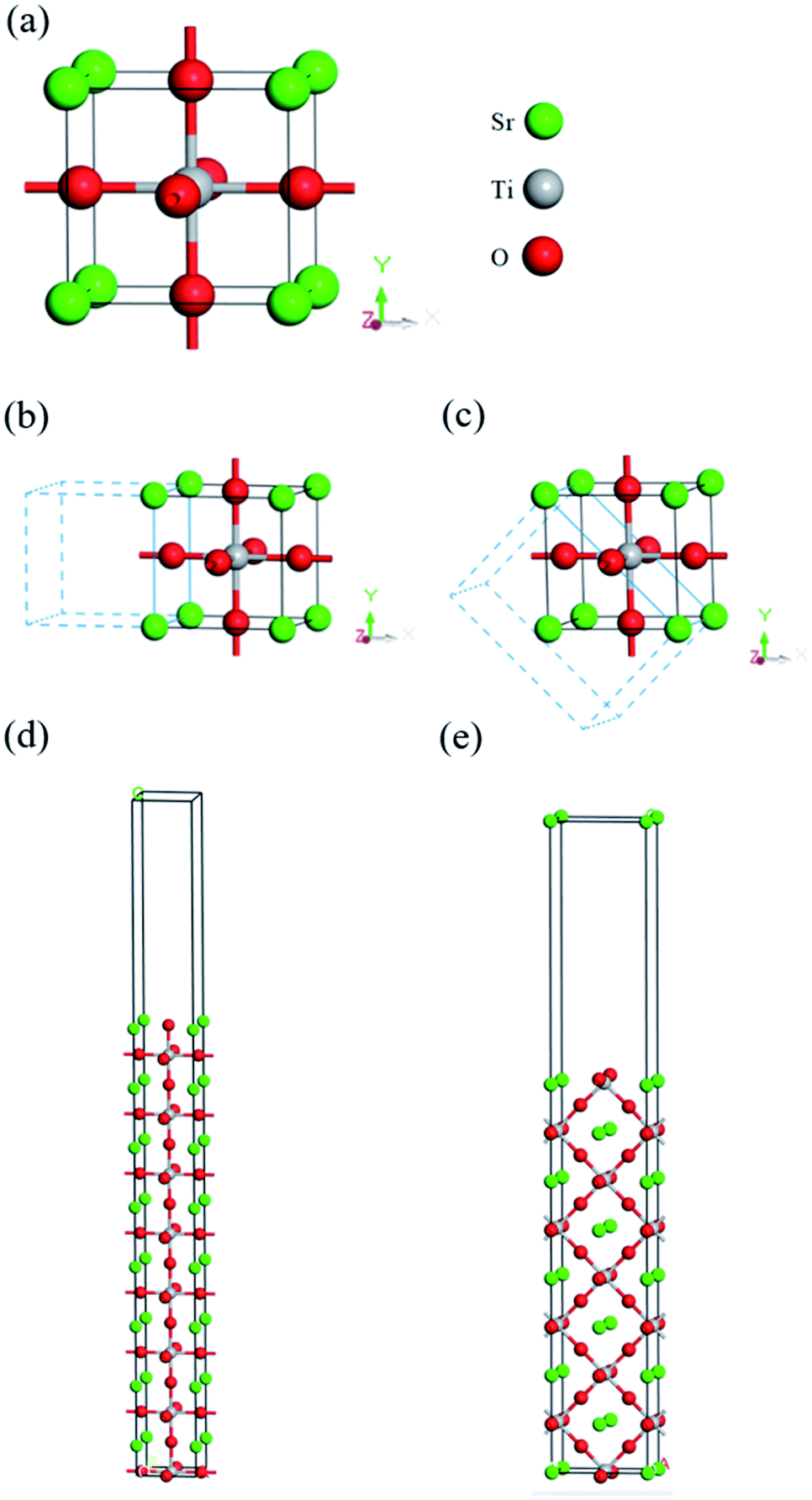 | ||
| Fig. 1 Models of cubic SrTiO3: (a) unit cell with lattice constant a = b = c = 3.905 Å, α = β = γ = 90.0°, (b) (100) plane, (c) (110) plane, and 8-layered superlattices of (d) (100) plane and (e) (110) plane. | ||
| XC-Functional | Computational method | Lattice constants | Eg (eV) | ||
|---|---|---|---|---|---|
| a/b/c (Å) | α/β/γ (°) | ||||
| Present work | PBE | GGA+Up+Ud | 3.905 | 90.00 | 3.252 |
| Other simulation results | PBE | GGA+Up+Ud | 3.919a | 90.00 | 3.222a |
| PBE | GGA+Up+Ud | 3.952b | 90.00 | 3.220b | |
| Experimental data | NA | NA | 3.905c | 90.00 | — |
| NA | NA | 3.910d | 90.00 | — | |
| NA | NA | — | — | 3.220e | |
| NA | NA | — | — | 3.250f | |
 | ||
| Fig. 2 Calculated (a) band structure and (b) PDOS of cubic SrTiO3. The Fermi level is set to 0 eV. GGA+Up+Ud correction is used to describe the localized transition with Up (4.20 eV) on O 2p and Ud (5.95 eV) on Ti 3d. The calculated band gap is 3.252 eV, and the VBM and CBM are characteristic of O 2p and Ti 3d. | ||
According to the results of Takata et al., the oxidative and reductive reactions primarily happen on {110} and {100} facets of 18-facet SrTiO3, respectively.71 Hence, in this work, the (100) and (110) crystal planes of SrTiO3, shown in Fig. 1(b)–(e), were chosen as representative models for the built-in potential estimation of the facet junction at the (110)/(100) interface. For each plane, the convergence of sufficient number of layers was tested to avoid surface reconstruction due to the different forces exerted on the internal atoms and the surface atoms. Theoretically, the MAEPs of the inner slab, the potential on the side of the vacuum region, for layered (110) and (100) should be identical after reaching convergence, as they are the same material. Therefore, the difference of the inner slab MAEPs between (100) and (110) are calculated for different layered structures shown in Fig. S1.† It can be seen that the difference of inner slab MAEPs between (100) and (110) will gradually reduce as the layers increase. However, when the MAEP difference reduces to about 0.885 ± 0.006 eV, it becomes almost steady and converged. Hence, the eight layered structure was chosen as Fig. S1† revealed that eight layers are enough to reach convergence of work function calculated for both (100) and (110) planes.
The formation of a facet junction is different from that of a conventional homojunction. The former is a result of different ordering of atoms in the crystal planes. The surface potentials of the two planes will be located at different positions, with the potential drop driving the charge flow. The latter is formed by doping holes or electrons in a host material to cause a difference in chemical potential (Fermi level) between p-type and n-type semiconductors and thus forming a p–n junction. However, the facet junction can be seen as a homojunction because it is only composed of one material. Therefore, in this work, eqn (1)–(4) are employed to calculate the built-in potential at the (110)/(100) facet junction in SrTiO3.
Normally, the built-in potential of a homojunction can be calculated by the work function difference between the two segments in conjunction. Therefore, the built-in potential at the (110)/(100) facet junction can be estimated with eqn (5).
| Vbi(110)/(100) = ϕ(110) − ϕ(100) | (5) |
The work function of the two planes are calculated based on electrostatic potential shown in Fig. 3, with values of 3.098 eV (100) and 6.168 eV (110), respectively. The resulting built-in potential is 3.07 V.
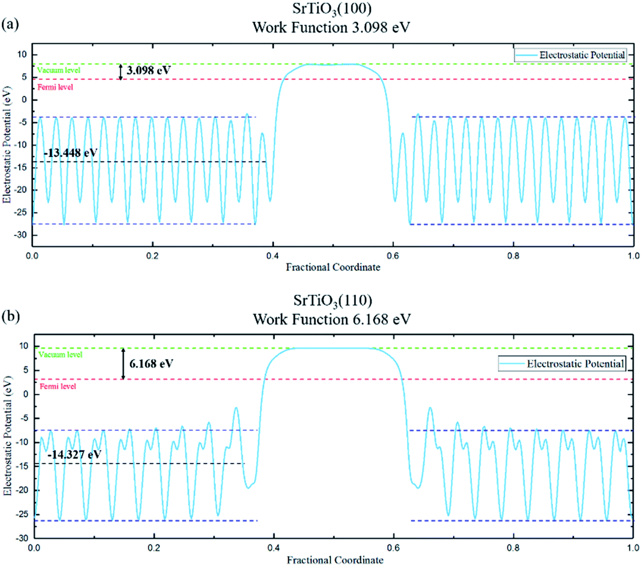 | ||
| Fig. 3 The average potential and work function (difference between vacuum level and Fermi level) of (a) (100) and (b) (110) planes. Green dashed line is vacuum level, red dashed line is Fermi level, dark blue dashed lines denote the upper/lower converged values of the side of the vacuum region, i.e., the inner slab, while black dashed line represents the MAEP of the inner slab. | ||
In addition, the electrostatic potential and band calculations of (110) and (100) facets are shown in Fig. S2 and S3.† The use of five repeating units for (110) and seven repeating units for (100) for construction of super lattice segments ensures the stability of energy variation for enough cycles. It can be seen that the PAEPs of (110) and (100) are very stable, and the MAEPs are both about −11.319 eV. The calculated band edges of (100) and (110) are the same, with VBM at 5.682 eV and CBM at 8.933 eV. Thus, the band gaps of both planes are 3.251 eV, which is consistent with the fact that they are just different arrangements of the same mono-crystal plane.
To further estimate the band offset of the (110)/(100) junction, a superlattice was built by joining the two segments, as shown in Fig. 4(a). The formation energy of the facet junction, Ef(110)/(100), has been calculated by eqn (6).
 | (6) |
 | ||
| Fig. 4 (a) Schematic and relaxed superlattice, (b) average electrostatic potential, and (c) band diagram of the (110)/(100) facet junction. The built-in potential is estimated at 2.913 eV, which is equal to the VBO and CBO. The p-type and n-type segments are formed by (110) and (100), respectively. | ||
After aligning the Fermi level, a clear potential drop of the MAEP exists across the (110)/(100) facet junction seen in Fig. 4(b), resulting in the generation of a built-in electric field. As the work function of (110) is higher than that of (100), the MAEP of (110) is higher as well. The values of the MAEPs are −9.736 eV for the (110) segment and −12.649 eV for the (100) segment, with a resulting built-in potential of 2.913 V calculated by eqn (4). This value is very close to the work function difference between pure (100) and (110) planes, with an error of about 5.39%. The complete band diagram of the junction is shown in Fig. 4(c). The values of CBO and VBO in the (110)/(100) facet junction are the same as the built-in potential since the facet junction is a homojunction, with no contribution of the band discontinuity, i.e., only built-in potential contributes to the band offsets. Additionally, the CBM and VBM of (110) segment is higher than that of (100) segment after forming the (110)/(100) facet junction, indicating that the p-type and n-type roles are played by (110) and (100) planes, respectively.
The electronic structures of the (110) and (100) planes are evaluated in the same manner as bulk SrTiO3, with Fig. 5(a)–(h) showing that in both of (110) and (100) planes, the VBM is determined by O 2p, and the VB is mainly composed of O 2s, O 2p, Sr 4p with small contribution from Ti 3d. On the other hand, the CBM is dominated by Ti 3d, and the CB is mainly contributed by d orbital in Ti and Sr atoms with slight O 2p contribution. From the calculations, it can be seen that both the VBM and CBM values of (110) are higher than that of (100), verifying the p-type and n-type characteristics of (110) and (100) after the facet junction is formed. In addition, compared with bulk SrTiO3, the peaks of all the atomic orbitals of the two planes are similar in energy as the bulk, with slight shifts as expected of surfaces. Also, the PDOS of the atoms in the bulk are compared with the atoms locate near the facet junction (atom selections are shown in Fig. S4†), shown in Fig. 6(a)–(h). The peaks of all atomic orbitals shifted to lower energy by approximately 2 to 5 eV after facet junction formation. Moreover, the PDOS of Ti 3d and Sr 4d in the (110)/(100) facet junction are broadened compared to that in bulk SrTiO3, shown in Fig. 6(c) and (f), with the same trend found in normalized total DOS of the bulk and the facet junction shown in Fig. S5.† The broadening in the PDOS of these orbitals provides more energy states for trapping electrons and promote charge separation in the facet junction. As a result, holes and electrons will mainly concentrate on (110) and (100), respectively, to form an effective p–n junction to separate charges. This interesting phenomenon is due to the varying work function of these crystal planes, caused solely by different atom distribution in the planes. Hence, the photogenerated electrons will migrate from (110) to (100), and photogenerated holes migrate in opposite direction. The simulation result is consistent with experimental results showing that the OER and HER will occur on {110} and {100} facets respectively, reported by Takata et al.71
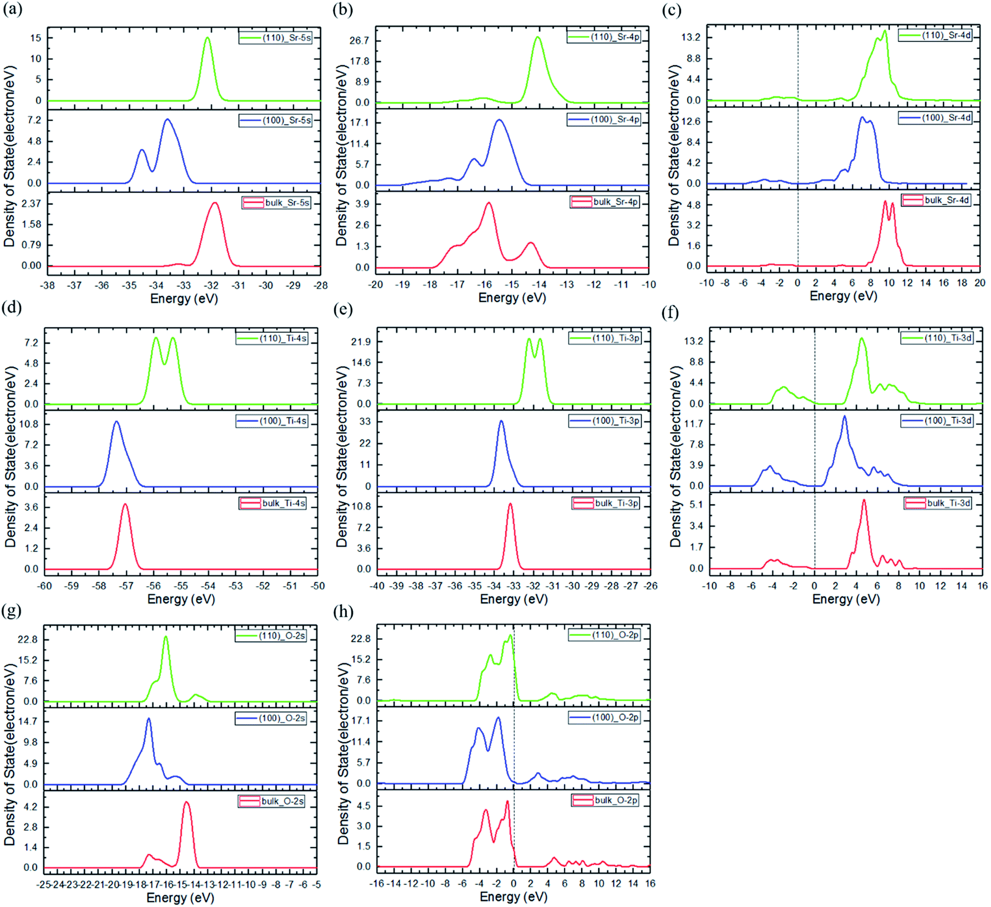 | ||
| Fig. 5 PDOS of bulk, (100) and (110) models: (a) Sr 5s, (b) Sr 4p, (c) Sr 4d, (d) Ti 4s, (e) Ti 3p, (f) Ti 3d, (g) O 2s, and (h) O 2p. Peaks of all the atomic orbitals of (110) and (100) are close to energies in the bulk, with slight shifts. Peaks in (100) are all shifted to lower energies compared to counterparts in (110), including O 2p and Ti 3d. The Fermi level is set to 0 eV. | ||
 | ||
| Fig. 6 PDOS of bulk atoms compared to those located near or on the facet junction for (a) Ti-4s, (b) Ti-4p, (c) Ti-3d, (d) Sr-5s, (e) Sr-5p, (f) Sr-4d, (g) O-2s, and (h) O-2p orbitals. Peaks for atoms in the junction are all shifted to lower energies compared to bulk. The width of Ti 3d and Sr 4d broadens after the facet junction is formed. The Fermi level is set to 0 eV. | ||
In this work, the result of estimated built-in potential of approximately 2.9 V for SrTiO3 which is very large compared to a standard silicon diode with a built-in potential of 0.7 V. This is also much higher than the many reported SrTiO3-based heterojunction structures, where values usually fall in the range of 0.9–1.2 V.72,73 Therefore, the built-in potential at the (110)/(100) facet junction is a very strong driving force for charge (electron/hole) separation, which is very important to the reaction efficiency of OER and HER. The results verified that the spontaneous forming of a built-in potential at the interface of anisotropic facet SrTiO3 can provide significant charge separation enhancement and can be completed in a mono-crystal without any dopant or band modulation.
4. Conclusions
The facet junction formed in anisotropic-fact catalyst is very important to charge separation in the photocatalysis. Though the band offsets at the facet junction in anatase TiO2 have been calculated, there is no direct theoretical estimation of built-in potential in such an anisotropic-facet photocatalyst. In this work, SrTiO3 is chosen, and the calculated band gap is in good agreement with experimental data. The result verified the reliability of calculation with GGA+Up+Ud method presented in this work. The built-in potential at the (110)/(100) facet function is estimated at 2.9 V using first principles calculations. It was revealed that different atom distribution on the crystal planes will cause a difference in work functions, and lead to the formation of a facet junction. The VBM and CBM of (110) and (100) were also calculated, and it was verified that the holes and electrons preferentially migrate to (110) and (100) planes, respectively. Thus, the OER and HER will occur on different planes with the separated electrons and holes. Through this work, the mechanism of the charge separation at the facet junction was elucidated, and demonstrated for the first time a method for estimation of built-in potential at the junction in anisotropic-facet materials. The technique can help in further design and development of efficient photocatalysts by means of anisotropic-facet engineering.Conflicts of interest
There are no conflicts to declare.Acknowledgements
The authors are grateful for the support provided by project (MOST 107-2221-E-007-047-MY3) from the Ministry of Science and Technology (MOST), Taiwan. We also appreciate the computational services provided by the National Center for High-performance Computing (NCHC), National Applied Research Laboratories (NAR Labs), Taiwan.References
- A. Fujishima and K. Honda, Nature, 1972, 238, 37 CrossRef CAS PubMed.
- S. Lin, H. Huang, T. Ma and Y. Zhang, Adv. Sci., 2020, 2002458 Search PubMed.
- L. E. Strange, J. Yadav, X. Li and S. Pan, J. Electrochem. Soc., 2020, 167, 146518 CrossRef CAS.
- R. Li, H. Chen, J. Xiong, X. Xu, J. Cheng, X. Liu and G. Liu, Materials, 2020, 13, 5057 CrossRef CAS PubMed.
- Parul, K. Kaur, R. Badru, P. P. Singh and S. Kaushal, J. Environ. Chem. Eng., 2020, 8, 103666 CrossRef CAS.
- T. Di, Q. Xu, W. Ho, H. Tang, Q. Xiang and J. Yu, ChemCatChem, 2019, 11, 1394 CrossRef CAS.
- K. Yang, X. Li, C. Yu, D. Zeng, F. Chen, K. Zhang, W. Huang and H. Ji, Chin. J. Catal., 2019, 40, 796 CrossRef CAS.
- N. Syed, J. Huang, Y. Feng, X. Wang and L. Cao, Front. Chem., 2019, 7, 713 CrossRef CAS.
- A. Kumar, M. Khan, J. He and I. M. C. Lo, Water Res., 2020, 170, 115356 CrossRef CAS PubMed.
- W. Zhang, A. R. Mohamed and W. J. Ong, Angew. Chem., Int. Ed., 2020, 59, 22894 CrossRef CAS PubMed.
- K. Perović, F. M. Rosa, M. Kovačić, H. Kušić, U. L. Štangar, F. Fresno, D. D. Dionysiou and A. L. Bozic, Materials, 2020, 13, 1338 CrossRef PubMed.
- Y. Li, M. Zhou, B. Cheng and Y. Shao, J. Mater. Sci. Technol., 2020, 56, 1 CrossRef.
- M. Du, S. Cao, X. Ye and J. Ye, J. Nanosci. Nanotechnol., 2020, 20, 5861 CrossRef CAS PubMed.
- B. Rhimi, C. Wang and D. W. Bahnemann, J. Phys.: Energy, 2020, 2, 42003 CAS.
- V. Hasija, P. Raizada, V. K. Thakur, A. A. P. Khan, A. M. Asiri and P. Singh, J. Environ. Chem. Eng., 2020, 8, 104307 CrossRef CAS.
- C. Wang and X. Zhang, Chem. Res. Chin. Univ., 2020, 36, 992 CrossRef CAS.
- M. Afshar, A. Badiei, H. Eskandarloo and G. M. Ziarani, Res. Chem. Intermed., 2016, 42, 7269 CrossRef CAS.
- D. Maarisetty and S. S. Baral, J. Mater. Chem. A, 2020, 8, 18560 RSC.
- R. Chen, S. Pang, H. An, T. Dittrich, F. Fan and C. Li, Nano Lett., 2019, 19, 18 Search PubMed.
- Y. Zhang, N. Afzal, L. Pan, X. Zhang and J. Zou, Adv. Sci., 2019, 6, 1900053 CrossRef PubMed.
- D. Maarisetty and S. S. Baral, J. Mater. Chem. A, 2020, 8, 18560 RSC.
- J. Nowotny, M. A. Alim, T. Bak, M. A. Idris, M. Ionescu, K. Prince, M. Z. Sahdan, K. Sopian, M. A. M. Teridi and W. Sigmund, Chem. Soc. Rev., 2015, 44, 8424 RSC.
- S. Bai, N. Zhang, C. Gao and Y. Xiong, Nano Energy, 2018, 53, 296 CrossRef CAS.
- M. Samadi, M. Zirak, A. Naseri, M. Kheirabadi, M. Ebrahimi and A. Z. Moshfegh, Res. Chem. Intermed., 2019, 45, 2197 CrossRef CAS.
- R. Malik and V. K. Tomer, Renewable Sustainable Energy Rev., 2021, 135, 110235 CrossRef CAS.
- L. Andronic and A. Enesca, Front. Chem., 2020, 8, 565489 CrossRef CAS PubMed.
- R. Fernández-Climent, S. Giménez and M. García-Tecedor, Sustainable Energy Fuels, 2020, 4, 5916 RSC.
- J. Huang, P. Yue, L. Wang, H. She and Q. Wang, Chin. J. Catal., 2019, 40, 1408 CrossRef CAS.
- A. Naldoni, M. Altomare, G. Zoppellaro, N. Liu, Š. Kment, R. Zbořil and P. Schmuki, ACS Catal., 2019, 9, 345 CrossRef CAS PubMed.
- H. Yu, L. Jiang, H. Wang, B. Huang, X. Yuan, J. Huang, J. Zhang and G. Zeng, Small, 2019, 15, 1901008 CrossRef PubMed.
- T. Bak, J. Nowotny, N. J. Sucher and E. Wachsman, J. Phys. Chem. C, 2011, 115, 15711 CrossRef CAS.
- M. Jørgensen, K. Norrman, S. A. Gevorgyan, T. Tromholt, B. Andreasen and F. C. Krebs, Adv. Mater., 2012, 24, 580 CrossRef PubMed.
- M. Jørgensen, K. Norrman and F. C. Krebs, Sol. Energy Mater. Sol. Cells, 2008, 92, 686 CrossRef.
- T. Ohno, K. Sarukawa and M. Matsumura, New J. Chem., 2002, 26, 1167 RSC.
- H. G. Yang, C. H. Sun, S. Z. Qiao, J. Zou, G. Liu, S. C. Smith, H. M. Cheng and G. Q. Lu, Nature, 2008, 453, 638 CrossRef CAS PubMed.
- J. Pan, G. Liu, G. Q. Lu and H. M. Cheng, Angew. Chem., Int. Ed., 2011, 50, 2133 CrossRef CAS PubMed.
- T. Tachikawa, S. Yamashita and T. Majima, J. Am. Chem. Soc., 2011, 133, 7197 CrossRef CAS PubMed.
- R. Li, F. Zhang, D. Wang, J. Yang, M. Li, J. Zhu, X. Zhou, H. Han and C. Li, Nat. Commun., 2013, 4, 1432 CrossRef PubMed.
- J. Zhu, F. Fan, R. Chen, H. An, Z. Feng and C. Li, Angew. Chem., Int. Ed., 2015, 54, 9111 CrossRef CAS PubMed.
- L. Mu, Y. Zhao, A. Li, S. Wang, Z. Wang, J. Yang, Y. Wang, T. Liu, R. Chen, J. Zhu, F. Fan, R. Li and C. Li, Energy Environ. Sci., 2016, 9, 2463 RSC.
- G. Liu, J. C. Yu, G. Q. Luc and H. M. Cheng, Chem. Commun., 2011, 47, 6763 RSC.
- Y. Zhang, H. Gong, Y. Zhang, K. Liu, H. Cao, H. Yan and J. Zhu, Eur. J. Inorg. Chem., 2017, 2017, 2990 CrossRef CAS.
- L. Shan, C. Lu, L. Dong and J. Suriyaprakash, J. Alloys Compd., 2019, 804, 385 CrossRef CAS.
- J. Yang, Y. Peng, S. Chen, B. Yang, Y. Liu, L. Peng and J. Zhang, Mater. Res. Express, 2019, 6, 85501 CrossRef CAS.
- Y. Luo, S. Suzuki, Z. Wang, K. Yubuta, J. J. M. Vequizo, A. Yamakata, H. Shiiba, T. Hisatomi, K. Domen and K. Teshima, ACS Appl. Mater. Interfaces, 2019, 11, 22264 CrossRef CAS.
- M. Li, S. Yu, H. Huang, X. Li, Y. Feng, C. Wang, Y. Wang, T. Ma, L. Guo and Y. Zhang, Angew. Chem., Int. Ed., 2019, 58, 9517 CrossRef CAS.
- S. J. Clark, M. D. Segall, C. J. Pickard, P. J. Hasnip, M. J. Probert, K. Refson and M. C. Payne, Z. Kristallogr., 2005, 220, 567 CAS.
- M. D. Segall, P. J. D. Lindan, M. J. Probert, C. J. Pickard, P. J. Hasnip, S. J. Clark and M. C. Payne, J. Phys.: Condens. Matter, 2002, 14, 2717 CrossRef CAS.
- J. P. Perdew, K. Burke and M. Ernzerhof, Phys. Rev. Lett., 1996, 77, 3865 CrossRef CAS.
- L. Wang, T. Maxisch and G. Ceder, Phys. Rev. B: Condens. Matter Mater. Phys., 2006, 73, 195107 CrossRef.
- M. Nolan and G. W. Watson, J. Chem. Phys., 2006, 125, 144701 CrossRef.
- X. Ma, Y. Wu, Y. Lv and Y. Zhu, J. Phys. Chem. C, 2013, 117, 26029 CrossRef CAS.
- J. Li, S. Meng, L. Li, H. Lu and T. Tohyama, Comput. Mater. Sci., 2014, 81, 397 CrossRef CAS.
- Y. Wang, C. Zhang, Y. Liu, M. Zhang and F. Min, Phys. Status Solidi B, 2019, 256, 1800574 CrossRef.
- Y. Q. Wang, W. Lian and Y. Liu, Optik, 2021, 228, 166128 CrossRef CAS.
- K. Lejaeghere, V. Van Speybroeck, G. Van Oost and S. Cottenier, Crit. Rev. Solid State Mater. Sci., 2014, 39, 1 CrossRef CAS.
- D. D. Koelling and B. N. Harmon, J. Phys. C: Solid State Phys., 1977, 10, 3107 CrossRef CAS.
- G. Kresse and J. Furthmüller, Phys. Rev. B: Condens. Matter Mater. Phys., 1996, 54, 11169 CrossRef CAS PubMed.
- H. J. Monkhorst and J. D. Pack, Phys. Rev. B: Solid State, 1976, 13, 5188 CrossRef.
- C. G. V. de Walle, Phys. Rev. B: Condens. Matter Mater. Phys., 1989, 39, 1871 CrossRef PubMed.
- C. G. V. de Walle and R. M. Martin, Phys. Rev. B: Condens. Matter Mater. Phys., 1986, 34, 5621 CrossRef.
- G. D. Liberto, S. Tosoni, F. Illas and G. Pacchioni, J. Chem. Phys., 2020, 152, 184704 CrossRef PubMed.
- G. D. Liberto, S. Tosoni and G. Pacchioni, J. Phys. Chem. Lett., 2019, 10, 2372 CrossRef.
- R. J. Nelmes, G. M. Meyer and J. Hutton, Ferroelectrics, 1978, 21, 461 CrossRef CAS.
- A. Janotti, B. Jalan, S. Stemmer and C. G. Van de Walle, Appl. Phys. Lett., 2012, 100, 262104 CrossRef.
- D. Xu, Y. Yuan, H. Zhu, L. Cheng, C. Liu, J. Su, X. Zhang, H. Zhang, X. Zhang and J. Li, Materials, 2019, 12, 138 CrossRef CAS PubMed.
- M. Cardona, Phys. Rev., 1965, 140, A651 CrossRef.
- K. van Benthem, C. Elsässer and R. H. French, J. Appl. Phys., 2001, 90, 6156 CrossRef CAS.
- M. Zacharias, M. Scheffler and C. Carbogno, Phys. Rev. B, 2020, 102, 45126 CrossRef CAS.
- M. Arai, S. Kohiki, H. Yoshikawa, S. Fukushima, Y. Waseda and M. Oku, Phys. Rev. B: Condens. Matter Mater. Phys., 2002, 65, 85101 CrossRef.
- T. Takata, J. Jiang, Y. Sakata, M. Nakabayashi, N. Shibata, V. Nandal, K. Seki, T. Hisatomi and K. Domen, Nature, 2020, 581, 411 CrossRef CAS.
- R. Comes and S. Chambers, Phys. Rev. Lett., 2016, 117, 226802 CrossRef.
- K. H. L. Zhang, R. Wu, F. Tang, W. Li, F. E. Oropeza, L. Qiao, V. K. Lazarov, Y. Du, D. J. Payne, J. L. MacManus-Driscoll and M. G. Blamire, ACS Appl. Mater. Interfaces, 2017, 9, 26549 CrossRef CAS PubMed.
Footnote |
| † Electronic supplementary information (ESI) available. See DOI: 10.1039/d1ra01711j |
| This journal is © The Royal Society of Chemistry 2021 |