
 Open Access Article
 This Open Access Article is licensed under a Creative Commons Attribution-Non Commercial 3.0 Unported Licence
Tunable photoluminescence and SERS behaviour of additively manufactured Au nanoparticle patterns†
Saleh Aghajani *,
Angelo Accardo and
Marcel Tichem
*,
Angelo Accardo and
Marcel Tichem
Delft University of Technology, Faculty of Mechanical, Maritime, and Materials Engineering (3ME), Department of Precision and Microsystems Engineering (PME), Mekelweg 2, Delft 2628 CD, The Netherlands. E-mail: S.Aghajani@tudelft.nl
First published on 6th May 2021
Abstract
The ability to tune the localised surface plasmon resonance (LSPR) behaviour of metal nanostructures has great importance for many optical sensor applications such as metal (plasmon) enhanced fluorescence spectroscopy and surface-enhanced Raman scattering (SERS). In this paper, we used Aerosol Direct Writing (ADW) to selectively deposit fine gold nanoparticles (AuNPs) patterns. A low-temperature thermal post-treatment (below 200 °C) provides enough energy to merge and transform AuNPs into larger features significantly different from non-thermally treated samples. The optical behaviour of non-treated and thermally treated AuNP films was investigated by photoluminescence (PL) spectroscopy. The PL measurements showed a red-shift, compared to bulk gold, using 488 nm and 514 nm laser excitation, and a blue-shift using 633 nm laser excitation. The thermal post-treatment leads to a further blue-shift compared to non-treated samples in the presence of both 514 and 633 nm laser. Finally, the AuNPs patterns were employed as a SERS-active substrate to detect low-concentrated (10−8 M) rhodamine B. This method's ability to selectively deposit 3D gold nanostructures and tune their optical behaviour through a low-temperature thermal treatment allows optimisation of the optical response and enhancement of the Raman signal for specific bio-analytes.
Introduction
Metal nanoparticles (MNPs) and metal nanostructures (MNSs) are used for detection purposes in optical biosensors due to their unique optical behaviours.1–5 Biosensors based on MNPs and MNSs allow simple, rapid, straightforward, and label-free detection of analytes and biomarkers in very low concentrations with high selectivity and sensitivity6–9 due to the electromagnetic field enhancement of the structures.8,10 The electromagnetic enhancement comes from the coherent oscillation of electron clouds, excited by incident light at the metal/dielectric interface. These collective oscillations are either confined on the surface of the metallic structure and referred to as surface plasmon resonance (SPR) or confined in nanometric features and referred to as localised surface plasmon resonance (LSPR).11,12 This effect has been used in detection methods such as surface-enhanced infrared absorption spectroscopy (SEIRAS),13 metal (plasmon) enhanced fluorescence (MEF/PEF),14–16 surface-enhanced Raman scattering (SERS) spectroscopy,17–20 and surface-enhanced resonance Raman scattering (SERRS) spectroscopy.21–23 SERS and SERRS are used in many applications because they can provide unique Raman spectroscopy fingerprints of low concentrated analytes down to micro and nanomolar.7,24For an ideal SERS-active substrate, a high enhancement of SERS signal, low limit-of-detection (LOD), high reproducibility of the SERS response, and low manufacturing cost are needed. This requires tailoring the size, shape, and density of nanostructures and selecting optimal material. The typical material for the fabrication of a SERS substrate is gold because of its visible range LSPRs and high chemical stability. Different methods are proposed for the fabrication of SERS-active substrates, such as electron beam lithography25 and photolithography.26 However, the complexity and multi-step processing nature of these methods increase the time and cost of fabrication of SERS-substrates. To overcome the complexity of the previous methods, different strategies have been developed to manufacture SERS substrates, such as nanosphere lithography (NSL),27–29 Langmuir–Blodgett technique,30 chemical reduction,31 self-assembly,32 and electrochemical deposition.33 However, all these methods use either wet processes, which involve the presence of different liquids, hazardous chemicals and high risk of contamination, or high temperature and expensive instruments. Moreover, for SERS bio-applications, the active surface ideally needs to be integrated into a microfluidic device, which requires the ability to manufacture SERS-active regions on the substrate selectively. In this work, we used our recently reported aerosol direct writing method (ADW)20 to create patterns of gold nanoparticles on a silicon substrate and study the effect of post-deposition thermal treatment on the morphology and photoluminescence of the deposited AuNPs patterns as well as the performance of these patterns as SERS-active substrates. The ADW method allows direct, spatially selective, one-step processing and robust deposition of metal or alloy NPs (with a particle size distribution of 0–20 nm) on a wide variety of substrates, including Si, polymers, paper, and glass. The technique allows fine control over the density of NPs and the resolution of the patterns through process parameters, such as the deposition speed and nozzle to substrate distance. The absence of any chemical for particle generation or stabilisation of NPs and the presence of argon as carrier gas prevents the introduction of impurities. The deposited AuNPs patterns, typically characterised by hills and valleys with hundreds of nanometers differences in height, form a porous 3D microstructure with nanometric features. We report the effect of low-temperature (below 200 °C) post-deposition thermal treatment resulting in a conversion of the nanoscale-roughness porous microstructure into larger nanostructure with smooth surfaces. Furthermore, we show that the evolution of morphology affects the AuNPs film's photoluminescence, especially when subjected to laser excitation of 514 nm and 632 nm, leading to a blue-shift in the peak compared to the non-treated deposited Au patterns. The deposited AuNPs demonstrated high SERS sensitivity in detecting Rhodamine B (RhB) as a probe molecule, with a 10−8 M and a 10−7 M detection limit under, respectively, laser excitation of 514 nm and 633 nm.
Materials and methods
Sample preparation
To fabricate SERS-active substrates, a previously developed experimental setup exploiting Aerosol Direct Writing (ADW)20 was used to deposit AuNPs in the form of patterns on a silicon substrate. In brief, the ADW setup consists of a commercial particle generator (VSParticle G1) and a vacuum deposition chamber. In this method, very fine and pure AuNPs with a polydispersed size distribution of 0 to 20 nm are generated by a spark ablation method (SAM) from gold electrodes (99.99% pure) and are carried to the deposition chamber in an argon flow. A 3D printed converging nozzle with 400 μm outlet diameter aerodynamically focuses the AuNPs and deposits them on the substrate by impaction. All substrates were first cleaned with acetone and isopropanol and, immediately before the deposition, placed in an oxygen plasma chamber for 30 minutes to remove any impurity on the substrate and to increase the adhesion of AuNPs upon deposition. This cleaned substrate is then mounted on the stage in the vacuum chamber perpendicular to the nozzle. The substrate's distance to the nozzle is controlled with an out-of-plane precise SmarAct SLC-1750-O20-D-HV positioner, while the in-plane deposition pattern is controlled with two SmarAct SLC-1750-M-E-HV positioners. Following the same configuration of process parameters for earlier copper nanoparticle deposition,20 all samples were prepared with a fixed nozzle to substrate distance of 400 μm, a flux of 1050 sccm of argon gas, 1 bar upstream pressure, a vacuum pressure of 275 ± 2% Pa, deposition speed of 80 μm s−1, SAM voltage and the current setting of V = 0.9 kV and I = 5 mA respectively. For thermal post-treatment, AuNPs patterned on silicon substrates were placed in a Binder VD23 Vacuum oven with a vacuum pressure of 0.01 mbar, with 8 different thermal treatment programs in terms of temperature and time, see Table 1. For each sample, two silicon substrates with two lines of AuNPs patterns were made.| Sample | Temperature (°C) | Time (min) |
|---|---|---|
| S 1 | — | — |
| S 2 | 100 | 15 |
| S 3 | 100 | 30 |
| S 4 | 100 | 120 |
| S 5 | 120 | 15 |
| S 6 | 120 | 30 |
| S 7 | 150 | 5 |
| S 8 | 150 | 15 |
| S 9 | 200 | 5 |
Morphology characterisation
To study the deposited patterns' morphology, white light interferometry, scanning electron microscopy (SEM), and atomic force microscopy (AFM) were used. The white-light interferometry was performed with a Contour GT-K 3D optical profilometer (Bruker Corporation, Billerica, MA, USA) with ∼10–50 nm resolution and an objective of 20×. Line profiles were obtained by integrating three measurements at each location. The white-light interferometry data were post-processed with GWYDDION 2.55 software to remove the effect of the background. The SEM measurements were performed with a field-emission high-resolution Helios G4, all with a secondary electron through-the-lens (TLD) detector. A JPK Nanowizard 4 coupled to a Zeiss microscope in QI mode was used for AFM measurements. High-resolution silicon AFM tips of SAA-SPI-SS were used from Bruker with the nominal resonant frequency of 55 kHz, force constant of 0.25 N m−1, an aspect ratio of at least 5![[thin space (1/6-em)]](https://www.rsc.org/images/entities/char_2009.gif) :1 in the last 100 nm, and a nominal curvature radius of 1 nm. The combination of the low radius probe and the tip's high aspect ratio enables high-resolution imaging of surfaces with substantial height differences, thus decreasing the possible convolution effect to the minimum. All AFM measurements were performed at room temperature with two scan areas of 1.0 × 1.0 and 0.25 × 0.25 μm2. GWYDDION 2.55 software was used for the post-processing of AFM measurements data.
:1 in the last 100 nm, and a nominal curvature radius of 1 nm. The combination of the low radius probe and the tip's high aspect ratio enables high-resolution imaging of surfaces with substantial height differences, thus decreasing the possible convolution effect to the minimum. All AFM measurements were performed at room temperature with two scan areas of 1.0 × 1.0 and 0.25 × 0.25 μm2. GWYDDION 2.55 software was used for the post-processing of AFM measurements data.
SERS and photoluminescence measurements
Photoluminescence and Raman spectroscopy measurements were performed on a Horiba LabRAM HR setup, equipped with an argon-ion laser operating at 488 and 514 nm, and a helium–neon laser operating at 633 nm, a liquid-nitrogen cooled CCD camera, and objectives of 50× (NA = 0.5) and 10× (NA = 0.25). The photoluminescence (PL) studies were performed using an objective of 10× and acquisition time of 20 s, with the previously mentioned lasers over 30 random locations within the AuNPs deposited patterns, including centric and boundary regions of the patterns. The two optical filters in the excitation laser path and the scattered response path from the sample remove any wavelength below the desired excitation lasers. The spectra were collected over the range of 450–750 nm for the 488 nm excitation laser, 500–750 nm for the 514 nm excitation laser, and 600–1000 nm for the 633 nm excitation laser.For SERS studies, different Rhodamine B (RhB) concentrations were prepared out of RhB powder, purchased from Sigma-Aldrich, diluted in deionised water. For a homogeneous and monolayer distribution of the probe molecule on the nanostructured surface, at first, the silicon substrate containing AuNPs patterns was immersed in the RhB solution for 12 hours to have sufficient molecules adsorbed the samples. Then, samples were removed from the solution and washed with deionised water to remove an excess of RhB and dried with nitrogen. Two laser excitations of 514 nm and 633 nm focused with an objective of 50× were used for the SERS study, and spectrums were acquired with an acquisition time of 10 s and integration of 2. Similar to PL studies, data were recorded using LabSpec6 software, and baseline subtraction was performed to remove the background. The SERS signal of RhB was recorded over the spectral range 500–1700 cm−1 with a spectral resolution of 0.6 cm−1. The Raman signal of RhB on AuNPs deposited patterns with and without heat treatment was measured at 160 different random locations within the patterns to assess the SERS signal's reproducibility.
Results and discussion
Morphology of deposited film
Fig. 1 shows the white light interferometry image of a line of deposited AuNPs on a silicon substrate. The colour indicates the height of the deposited features, and, at specific locations, sudden peaks can be observed. This can also be seen in the 3D image of the line in Fig. 1b and the cross-sectional profile in Fig. 1(c1–c5). Peaks are related to agglomerates of primary nanoparticles or microparticles. Primary nanoparticles carried in argon gas from the generation site to the deposition site start to agglomerate by impaction or columbic forces, creating larger particles with random sizes and shapes. These agglomerates of AuNPs are characterised by higher mass and inertia; therefore, they will deposit mainly in the central region, as confirmed in Fig. 1a. Next to agglomerates of AuNPs, gold microparticles also exist in the flow related to molten gold ejection from electrodes.34,35 These microparticles are more than 500 nm diameter in size with a spherical shape, as shown in Fig. S1a–c,† they will deposit as well more often in the centric region due to their higher inertia.20 | ||
| Fig. 1 (a) White-light interferometry image of a line of AuNPs deposited on a silicon substrate, (b) 3D view of the line, (c1–c5) profile of the line at five sections showed in (a) with a Gaussian fit. The AuNPs were deposited with SAM voltage/current setting of V = 0.9 kV and I = 5 mA, the nozzle to substrate distance of 400 μm and deposition speed of ∼120 μm s−1. | ||
In ADW, particles are carried to the deposition chamber via the argon gas, and their final localisation on the substrate depends on their mass and velocity when leaving the nozzle system. The velocity depends on the NP's position relative to the nozzle's centreline since the gas' velocity profile has a maximum at the centreline and has zero velocity on the nozzle's wall. Therefore, particles closer to the centreline have higher velocity and higher inertia; hence they will more likely deposit on the substrate. Likewise, particles further away from the centreline and closer to the nozzle wall reach lower velocity due to a lower flow velocity; they will less likely deposit, particularly if their mass is small. Consequently, most particles in the centric region of the flow ended up on the substrate and formed the centric region of the patterned line (a yellowish region in Fig. 1a). Concerning particles far from the centric region of the flow, the majority of them follow the flow and do not deposit, while a minority of them deposit on the substrate but in a broader region (a white-bluish region in Fig. 1a). Therefore, the centric region of the line has a higher density of particles than the boundary of the deposited line and causes a Gaussian-like height distribution in the cross-sectional profile, as shown in Fig. 1(c1 to c5). See Fig. S2(a1 and a2)† for comparison between centric region and boundaries.
Fig. 2(a1) shows a deposited film of AuNPs on a silicon substrate and the film's characteristic morphology in a high-magnification SEM image. The film consists of dense and randomly shaped microstructures formed by aggregation of primary NPs with various sizes and agglomerates, resulting in a high-porosity three-dimensional (3D) structure with nanometric features. These microstructures have valleys and peaks with hundreds of nanometers difference in height, as indicated in AFM Fig. 3a and S3a.†
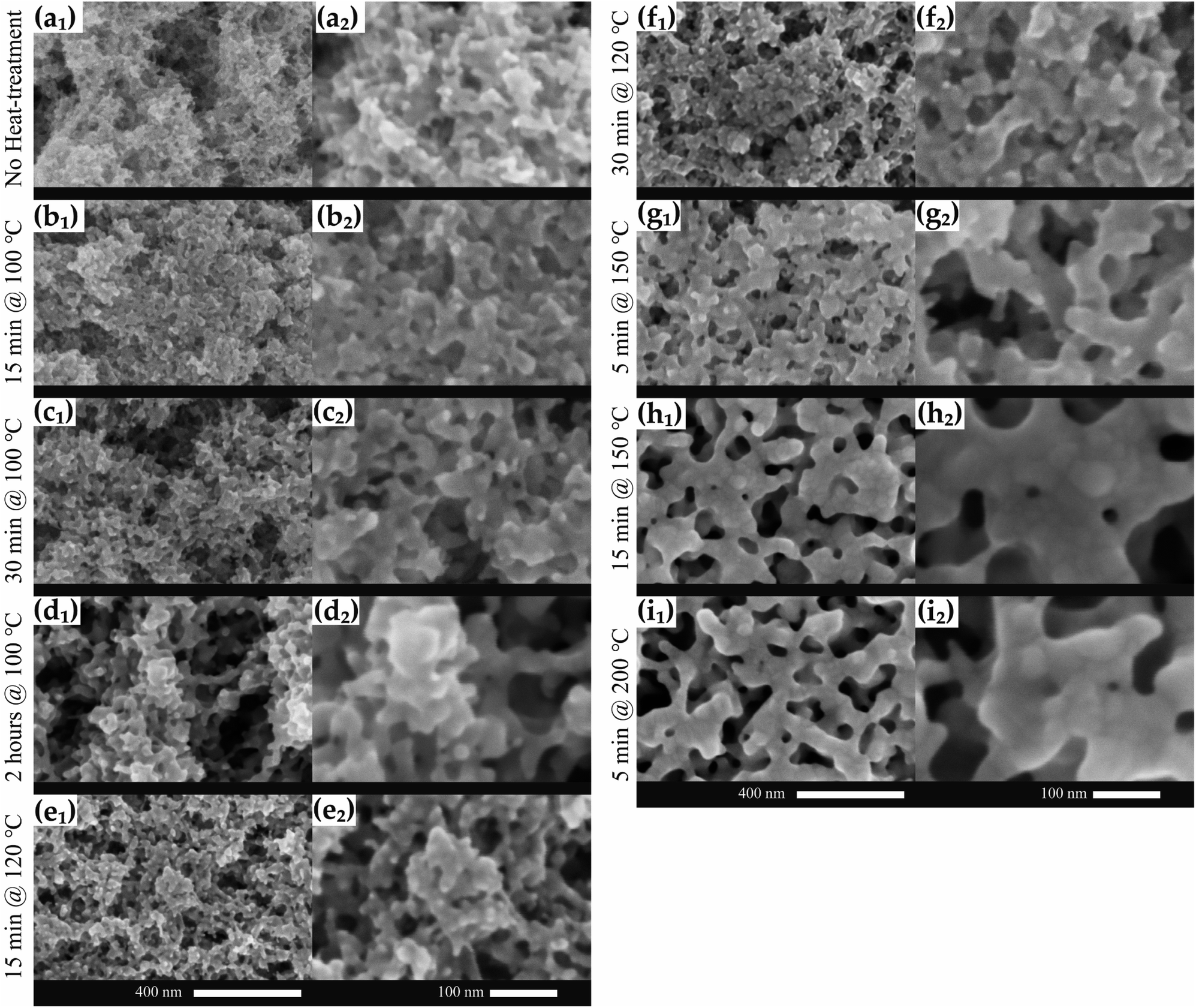 | ||
| Fig. 2 (a1 and a2) SEM images of the morphology of AuNPs deposited on a silicon substrate and transformation of the morphology (b–i) after thermal post-treatment in a vacuum environment. All AuNPs deposited with SAM voltage/current setting of V = 0.9 kV and I = 5 mA. | ||
 | ||
| Fig. 3 AFM morphology of 1.0 × 1.0 μm2 areas of (a) non-heat treated samples (b) 15 minutes at 100 °C, (c) 30 minutes at 100 °C, (d) 120 minutes at 100 °C, (e) 15 minutes at 120 °C, (f) 30 minutes at 120 °C, (g) 5 minutes at 150 °C, (h) 15 minutes at 150 °C, (i) 5 minutes at 200 °C. | ||
The transformation of the deposited film's surface morphology by different thermal post-treatment is summarised in SEM images in Fig. 2b–i, AFM images in Fig. 3b–i and S3b–i.† Comparing SEM images in Fig. 2(a2–f2) and AFM images in Fig. 3a–f, it is possible to see that temperature as high as 120 °C is not enough for inducing the coalescence of AuNPs and a significant change in the morphology of the AuNPs film, even by increasing the time of thermal treatment. Increasing the temperature to 150 °C, AuNPs start to merge, and larger structures are formed as depicted by SEM (Fig. 2(g1 and g2)) and AFM (Fig. 3g and S3g†). The further increase of thermal treatment time at 150 °C from 5 to 15 minutes promotes the coalescence of AuNPs and the formation of a morphology containing larger nanostructures and voids (Fig. 2(h1, h2), 3h and S3h†). A similar microstructure is formed in the samples thermally treated at 200 °C for 5 minutes, as shown in Fig. 2(i1, i2) and 3i. Looking at the high-magnification SEM images of Fig. 2(h2 and i2), it is observable that small particles merged to form larger structures, but their boundary is still visible and not entirely reshaped.
The temperatures used for the thermal post-treatment are much lower than the bulk melting temperature of gold (1064 °C) but high enough to trigger the coalescence of AuNPs, and the consequent evolution of the film's morphology. Nanoparticles have lower melting temperatures than their bulk counterpart, primarily due to a higher surface-to-volume ratio.36,37 This effect becomes more evident when particles' size becomes smaller than 20 nm.36 Moreover, the impaction deposition on a substrate as a result of ADW forms a dense, highly compacted AuNP film, which can play a positive role in the coalescence of neighbouring particles in the early stage of sintering.38
Photoluminescence experiment of the deposited film
To study the effect of thermal post-treatment on the optical behaviour of AuNPs film, photoluminescence (PL) spectroscopy with three laser excitations was employed. 30 PL spectrums were randomly measured in the cross-section of the line for each non-treated and heat-treated samples, along with the PL spectrum of bulk gold in response to laser excitations of 488 nm, 514 nm, and 633 nm (Fig. S4, S6, and S8†). The PL spectrum of each sample under different laser excitations shows that there are variations in the intensities. To compare the shape of the PL spectrums and their peak position, each spectrum was normalised with its peak intensity; therefore, all spectrums have a maximum unity (Fig. S5, S7, and S9†). Fig. S5, S7 and S9† show the normalised PL spectrums for all samples under different laser excitation, and it can be seen that the normalised PL spectrums of all 30 points for each sample are approximately similar. This similarity in each sample's shape and peak position indicates that the optical property in the line's cross-section is consistent; however, the AuNPs density and particle distribution are different in the line's cross-section. Therefore variation in the intensity of the non-normalised PL spectrum can be regarded as the difference in the density of AuNPs in the centric region of the line compared to the boundary region as depicted in Fig. S2.†Fig. 4 shows the averaged PL spectrum for each sample, using 30 normalised PL spectrums, along with one for bulk gold under different laser excitations. As shown in Fig. 4a and S5a–i† for laser excitation of 488 nm, spectrums of AuNPs deposited samples have similar shapes, consisting of a broad peak centred around 600–605 nm (2.049–2.066 eV) (Table 2). Comparing these results with the PL spectrum of bulk gold (Fig. S5j†), the spectral distribution broadened, and the intensity red-shifted about 110 nm (455 meV), as recorded in Table 2. This red-shift in the PL spectrum of AuNPs compared to bulk gold can be attributed to the localised surface plasmon resonance in the AuNPs film's nanostructure. Additionally, the similarity in the shape and peak position of PL spectrums of thermally treated samples compares to non-thermally treated samples indicates that the AuNPs have a weak plasmonic response under 488 nm laser excitation. This weak plasmonic response is also consistent with extinction spectrums of gold nanoparticles with different sizes calculated based on the Mie theorem.39,40
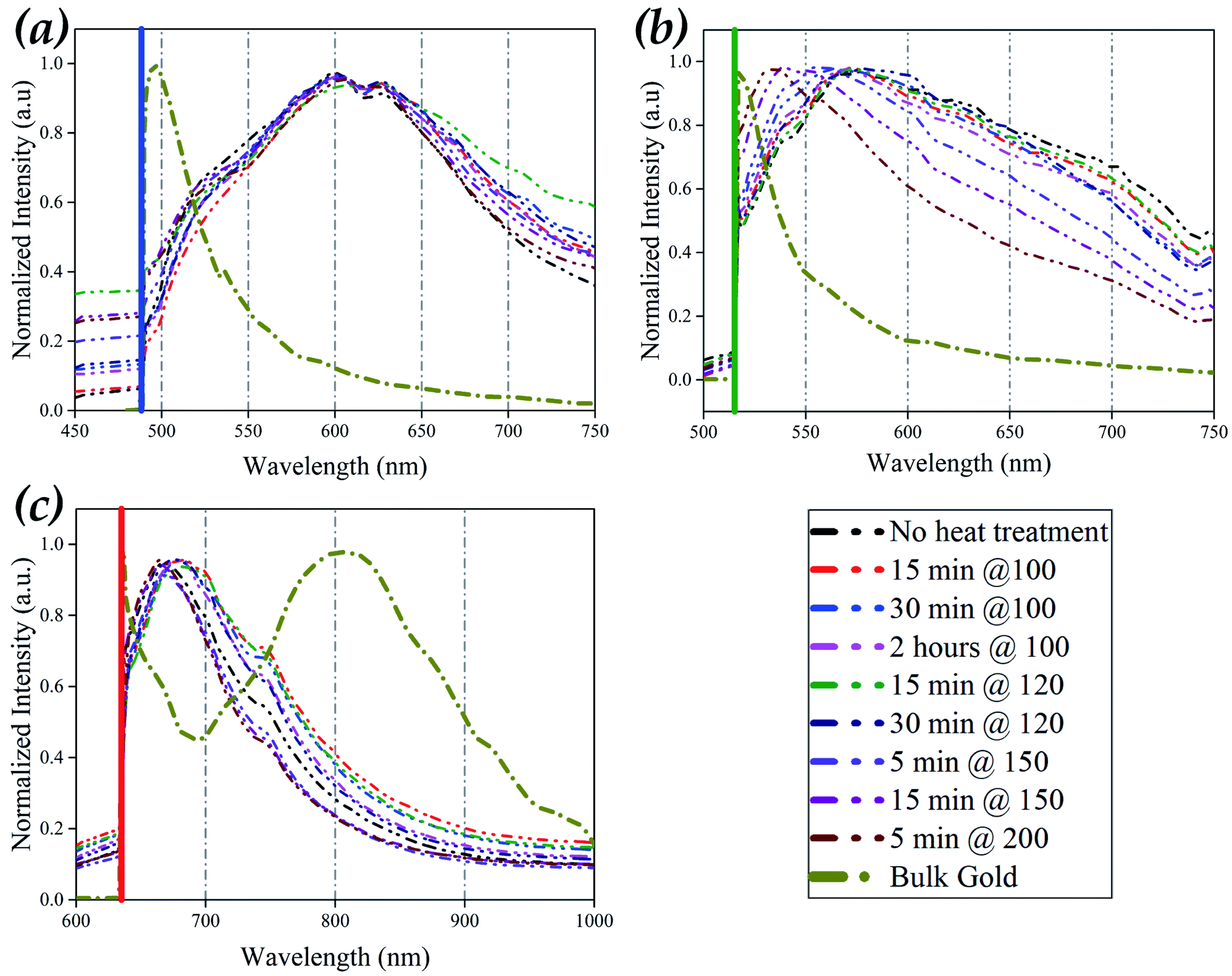 | ||
| Fig. 4 The average and normalized photoluminescence response spectrums of non-thermally treated and heat-treated samples compare to bulk gold at excitation laser of (a) 488 nm (b) 514 nm (c) 633 nm. PL measurement conditions: grating of 600 g cm−3, objective lens = 10× (NA = 0.25); for 488 nm laser: acquisition time = 20 s, integration time = 1; for 514 nm laser: acquisition time = 10 s, integration time = 2; 633 nm laser: acquisition time = 10 s, integration time = 1. For all lasers, 30 measurements (3 in length × 10 in cross-section) were performed, and the spectrums were normalized by the highest peak. All AuNPs deposited with SAM voltage/current setting of V = 0.9 kV and I = 5 mA. | ||
| Sample | Peak position under laser excitation of 488 nm (nm) – (eV) | Peak position under laser excitation of 514 nm (nm) – (eV) | Peak position under laser excitation of 633 nm (nm) – (eV) |
|---|---|---|---|
| No heat treatment | 600–2.066 | 577–2.148 | 668–1.856 |
| 15 minutes at 100 °C | 601–2.063 | 571–2.171 | 683–1.815 |
| 30 minutes at 100 °C | 601–2.063 | 569–2.179 | 679–1.825 |
| 2 hours at 100 °C | 602–2.059 | 571–2.171 | 677–1.831 |
| 15 minutes at 120 °C | 603–2.056 | 573–2.163 | 680–1.823 |
| 30 minutes at 120 °C | 601–2.063 | 573–2.163 | 677–1.831 |
| 5 minutes at 150 °C | 601–2.063 | 555–2.234 | 666–1.861 |
| 15 minutes at 150 °C | 603–2.056 | 539–2.300 | 665–1.864 |
| 5 minutes at 200 °C | 603–2.056 | 535–2.317 | 664–1.867 |
| Bulk gold | 495–2.504 | — | 800–1.549 |
Fig. 4b shows that the thermal post-treatment significantly affects the PL responses of AuNPs deposited film under 514 nm laser excitation. The PL spectrum of the sample without heat-treatment (Fig. S7a†) has a broad spectrum with maximum luminescence intensity around 577 nm (2.148 eV), which red-shifted about 60 nm (250 meV) compared to bulk gold (Fig. S7j† and Table 2). Thermal-treatments of 100 °C with a duration of up to 2 hours and 120 °C for 30 minutes (Fig. S7b–f†) have no significant effect on the PL spectrum's shape and peak position. However, a further increase in the thermal treatment's temperature or time leads to a significant blue-shift in the luminescence's peak and narrowing the PL spectrum compared to the non-treated AuNPs sample. The PL peaks' position of samples with heat treatment of 5 minutes and 15 minutes at 150 °C and 5 minutes at 200 °C are 555 nm (2.23 eV), 539 nm (2.3 eV), and 535 nm (2.317 eV), respectively (Fig. S7g–i† and Table 2). Considering the PL spectrums of heat-treated samples, it is observable that heat-treatment causes optical behaviour to move towards the bulk behaviour.
As shown in Fig. 4c and recorded in Table 2, the luminescence spectrum of bulk gold under 633 nm laser excitation has a broad peak at about 800 nm (1.549 eV). Fig. 4c and S9a–i† show a significant blue-shift of an average 130 nm (300 meV) and narrowing in the PL spectrum distribution of the AuNPs deposited film, with or without heat-treatment, compared to bulk gold. Additionally, heat-treatment of over 150 °C leads to PL spectrums with a peak centred around 666 nm (1.861 eV) and a narrower spectrum compared to other heat-treated and non-thermally treated samples. In contrast to the heat-treatment effect on the PL spectrum of AuNPs under 514 nm laser excitation, in 633 nm, heat-treatment causes a more pronounced peak in the PL spectrum far from the bulk spectrum.
SERS experiments on rhodamine B
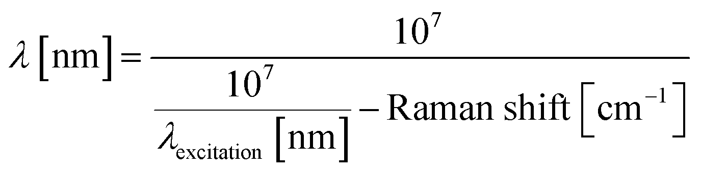
To evaluate the AuNPs film's efficiency as a SERS-active substrate, a series of Raman measurements were performed on different Rhodamine B (RhB) concentrations as a probe molecule. Rhodamine B's characteristic Raman peaks lie in the range of 550–1700 cm−1, namely 621 cm−1 (for xanthene ring deformation), 1199 cm−1 and 1279 cm−1 (for C–C bridge band stretching and aromatic C–H bending), 1358 cm−1 (for aromatic C–C bending) and 1648 cm−1 (for aromatic C–C bending and C![[double bond, length as m-dash]](https://www.rsc.org/images/entities/char_e001.gif) C stretching), which were considered in this study for SERS characterisation. The Raman spectral range can be converted from wavenumber into an absolute wavelength using eqn (1) as a laser excitation wavelength function. For 488 nm laser excitation, the RhB spectral range lies in the range of 501.5–532.5 nm; for 514 nm laser excitation, the RhB spectral range is 529.5–564 nm, and for 633 laser excitation, the RhB spectral range is 655.8–709.5 nm. Regarding the relative position of PL peak of AuNPs film and Raman spectral range of RhB, 514 nm and 633 nm laser excitations were chosen for the Raman experiment. A total of 160 Raman measurements (20 points in the cross-section of line and eight different cross-sections) were performed on AuNPs film for different concentrations of RhB.
C stretching), which were considered in this study for SERS characterisation. The Raman spectral range can be converted from wavenumber into an absolute wavelength using eqn (1) as a laser excitation wavelength function. For 488 nm laser excitation, the RhB spectral range lies in the range of 501.5–532.5 nm; for 514 nm laser excitation, the RhB spectral range is 529.5–564 nm, and for 633 laser excitation, the RhB spectral range is 655.8–709.5 nm. Regarding the relative position of PL peak of AuNPs film and Raman spectral range of RhB, 514 nm and 633 nm laser excitations were chosen for the Raman experiment. A total of 160 Raman measurements (20 points in the cross-section of line and eight different cross-sections) were performed on AuNPs film for different concentrations of RhB.
 | (1) |
The first sets of experiments are related to RhB detectability, the limit-of-detection (LOD), and the SERS signal's reproducibility on the AuNPs patterns deposited on a silicon substrate. Fig. 5a and b reports the Raman spectrum of RhB with concentrations of 1.0 × 10⁻³, 1.0 × 10⁻⁵, 1.0 × 10⁻⁶, 1.0 × 10⁻⁷, and 1.0 × 10⁻⁸ M, averaged over 160 measured spots under laser excitation of 514 nm and 633 nm, respectively. Comparing the SERS signal of RhB under different laser excitations shows that different characteristic peaks of RhB have different enhancement. This selective enhancement may be related to the relative position of LSPRs in the AuNPs films to the Raman spectral range of RhB. Considering the 621 cm−1, as the weakest characteristic peaks of RhB under excitation of 514 nm, appeared evidently from 1.0 × 10⁻³ to 1.0 × 10⁻⁷ M of RhB. At the concentration of 1.0 × 10⁻⁸ M, the 621 cm−1 peak is not observable, but the peak of 1648 cm−1 as the strongest peak is present; hence the LOD can be considered as 1.0 × 10⁻⁸ M. Using 633 nm laser excitation, all characteristic peaks are distinctively present in concentration as low as 1.0 × 10⁻⁷ M. But reducing the concentration to 1.0 × 10⁻⁸ M, the background data make the characteristic peaks of RhB less evident.
 | ||
| Fig. 5 Averaged Raman spectrums of 160 measurements on the RhB with concentrations of 1.0 × 10⁻³, 1.0 × 10⁻⁵, 1.0 × 10⁻⁶, 1.0 × 10⁻⁷, and 1.0 × 10⁻⁸ M RhB adsorbed on AuNPs patterns (a) under laser excitation of 514 nm and, (b) under laser excitation of 633 nm, (the inset in a and b is related to the concentration of 1.0 × 10⁻⁷ and 1.0 × 10⁻⁸ M RhB). Raman intensities and distribution of 160 main characteristic peaks of RhB at different concentrations under laser excitation of (c) of 514 nm and (d) 633 nm. Raman measurement conditions for 514 nm argon-ion laser and 633 nm He–Ne laser; acquisition time = 10 s, integration = 2; objective lens = 50× (NA = 0.5). | ||
Fig. 5c and d shows the correlation of the main characteristic peaks of RhB with the concentration of the RhB. Comparing the main characteristic peaks of RhB under the laser excitation wavelength of 514 nm and 633 nm, all characteristic peaks decreased about 2 cm−1 in the presence of the 633 nm laser, as depicted in Fig. 5c and d. This might be related to the shift in the peaks due to the enhanced resonance Raman scattering41,42 effect for 514 nm laser excitation as RhB has a sharp peak at 552 nm in UV-vis absorption,43,44 which is close to the 514 nm excitation laser. It can be seen from Fig. 5c and d that for each characteristic peak and concentration, there is a distribution of intensities, which shows the level of reproducibility of the SERS signal for RhB. The SERS signal distribution for similar concentration and corresponding characteristic peak shows that the 633 nm laser excitation leads to a broader intensity than 514 nm, yet both lasers have a good reproducibility level. Moreover, the results indicate that the Raman intensity of each characteristic peak increases with the concentration of RhB. A relatively good linear relationship was obtained between intensity and log[concentration] in the range of 10−3 M to 10−7 M for all characteristic peaks, with R2 in the range of 0.95–0.98.
Interestingly, the slopes of the lines at Fig. 5c and d under the same wavelength are different for different characteristic peaks, indicating that the SERS enhancement has a different effect on different vibrational modes. Under the wavelength of 514 nm, the Raman characteristic peaks of RhB have higher enhancement by increasing their wavenumber, i.e., 621 cm−1 has the lowest enhancement and 1648 cm−1 has the highest enhancement. Additionally, the slope of 1648 cm−1 is 1354 and 6 times higher than the slope of 621 cm−1, which shows that the 1648 cm−1 vibrational mode has a higher enhancement at a lower concentration than 621 cm−1. However, under excitation of 633 nm, the slope of the line has a narrower range between 320 at 1197 cm−1 646 for 619 cm−1 and 691 for 1646 cm−1.
The second set of experiments is related to the effect of different thermal post-treatments on the SERS performance and enhancement of AuNP films using 1.0 × 10⁻⁶ M RhB under laser excitation of 514 and 633 nm. Fig. 6a and b show that all characteristic peaks of RhB are distinguishably present for both laser excitations and all heat-treatments. The distributions of 160 intensities for each characteristic peak and laser excitations of 514 nm and 633 nm depicted in Fig. 6c and d show that all characteristic peaks of thermally treated samples follow approximately the same trends. For example, all characteristic peaks of samples heat-treated at 150 °C for 15 minutes have almost the same distribution level and compared to corresponding peaks in other samples have the same relations. Considering the results in Fig. 6, it can be seen that samples with no heat-treatment and heat-treatment of 2 hours at 100 °C have better performance than other heat-treatments for the detection of low-concentrated RhB under both laser excitations, with slightly a narrower distribution of 2 hours at 100 °C. Increasing the thermal treatment temperature to 120 °C leads to more uniform intensity distributions for the 514 nm laser, and, for the 633 nm laser, this happens at the thermal treatment of 150 °C and 15 min. At the same time, both heat-treatments have the lowest intensities in their corresponding laser excitation. The SERS performance results indicate that heat-treatment leads to a different effect on AuNP films than copper nanoparticles film and does not enhance the SERS signal of RhB20 as it did for copper SERS substrate.
 | ||
| Fig. 6 Averaged Raman spectrums of 160 measurements on the RhB with concentrations of 1.0 × 10⁻⁶, RhB adsorbed on AuNPs samples without heat-treatment and heat-treatment of 2 hours at 100 °C, 15 minutes at 120 °C, 30 minutes at 120 °C, 15 minutes at 150 °C, 5 minutes at 200 °C (a) under laser excitation of 514 nm and, (b) under laser excitation of 633 nm. Raman intensities and distribution of 160 main characteristic peaks of RhB on different samples (c) under laser excitation of 514 nm and (d) under laser excitation of 633 nm. Raman measurement conditions for 514 nm argon-ion laser and 633 nm He–Ne laser; acquisition time = 10 s, integration = 2; objective lens = 50× (NA = 0.5). | ||
Comparing the SERS results of different samples in Fig. 6c and d indicates that, surprisingly, samples have different intensity distributions for each laser. In Fig. 6c, samples with heat treatments of 2 hours at 100 °C and 15 minutes at 120 °C have the lowest distributions and samples of 15 minutes at 150 °C and 5 minutes at 200 °C have the highest distribution in the intensities of the characteristic peaks. However, an opposite trend is observable for laser excitation of 633 nm in Fig. 6d, which may be related to the relative position of AuNPs' LSPR to the laser excitation wavelength. Therefore, using the same sample may result in different distribution under 514 nm or 633 nm laser excitations.
Conclusions
The results of this work demonstrate: (1) the potential of the aerosol direct writing (ADW) method to deposit very fine gold nanoparticles with a size distribution of 0–20 nm on selected regions on a substrate; (2) the ability to tune the optical behaviour of the deposited film through low-temperature thermal treatment; (3) the suitability of the deposited metal nanoparticles (MNPs) patterns as SERS sensors. The advantage of directly coupling the nanoparticle generator unit with the deposition chamber enables solvent-free additive manufacturing of selectively deposited metal nanoparticles and alloys on wide ranges of substrates, without any need for surface functionalisation or conditioning chemicals in usual wet nanoparticle suspensions.We demonstrated that AuNPs patterns created by ADW on a silicon substrate have a Gaussian-shaped height distribution containing randomly formed microstructures of hundreds of nanometres' heights. These microstructures are formed by impaction of primary AuNPs or agglomerates of AuNPs on the substrate, caused by the kinetic energy they gained in the converging nozzle, and formed a high-porosity three-dimensional (3D) structure with nanometric features.
We also reported that a low-temperature thermal post-treatment affects the AuNPs patterns' morphology and their optical properties. SEM and AFM imaging revealed that temperatures much lower than the bulk melting point of gold are high enough to alter the microstructure of AuNPs, due to the extremely fine sizes of AuNPs and densely packed nanostructure. The results indicated that at temperatures as low as 150 °C and up to 200 °C, AuNP films' microstructure significantly evolves to form a nanostructure containing voids and networks of bridges. Concerning the optical properties of the manufactured films, photoluminescence (PL) measurement under three laser excitations of 488 nm, 514 nm, and 633 nm shows that the AuNPs patterns have significantly different optical behaviour than bulk gold. Moreover, thermally treated samples' optical behaviour alters with changing the time or temperature of thermal treatment, especially for temperatures higher than 150 °C and under laser excitation of 514 nm and 633 nm.
Finally, we explored AuNPs patterns' efficiency as a SERS-active substrate to detect low-concentrated Rhodamine B (RhB) as a probe molecule. We demonstrated that limit-of-detection (LOD) as low as 1.0 × 10⁻⁸ M could be achieved using a 514 nm laser excitation and 1.0 × 10⁻⁷ with a 633 nm laser. The stronger enhancement of RhB under laser excitation of 514 nm indicates that surface-enhanced resonance Raman scattering is involved in this process. We observed linear relation between the logarithmic concentration of RhB and the intensity of different characteristic peaks of RhB in the range of 1.0 × 10⁻⁷ to 1.0 × 10⁻³ with high coefficients of determination for all characteristic peaks. Moreover, we demonstrated the uniformity of the Raman signal of RhB in 160 random positions on the AuNPs patterns. Although a high level of uniformity of SERS signal is achieved in this study, it should be mentioned that this distribution in SERS signals is related to the distribution of hot-spots on the substrate and the defocusing of the laser beam on the substrate.
Although the heat-treatment of AuNPs did not lead to a significant enhancement of the Raman signal as happened in our previous copper nanopatterns,20 the ability to control the optical behaviour of AuNPs with a simple heat-treatment leads to the fabrication of SERS-active substrates enabling the resonance Raman scattering of analytes with different UV-vis peaks. This simple tunability of the morphology and, consequently, the metallic nanostructure's optical behaviour through a low-temperature thermal treatment could allow in the future to fabricate patterns with desired optical behaviour. Furthermore, the ability of ADW to selectively deposit nanoparticles of different metals and alloys on wide ranges of substrates (Si, glass, paper, and polymer) and integrability with other manufacturing techniques facilitate the fabrication of new on-chip SERS sensors.
Conflicts of interest
There are no conflicts to declare.Acknowledgements
The authors would like to thank Patrick van Holst, Gideon Emmanuel, Spiridon van Veldhoven and Rob Luttjeboer for their technical assistance. This project was supported by funding from the Delft University of Technology through the Nano Engineering Research Initiative (NERI, https://www.tudelft.nl/neri).References
- M. Liebel, N. Pazos-Perez, N. F. van Hulst and R. A. Alvarez-Puebla, Nat. Nanotechnol., 2020, 15, 1005–1011 CrossRef PubMed.
- C. Fang, A. Agarwal, K. D. Buddharaju, N. M. Khalid, S. M. Salim, E. Widjaja, M. V. Garland, N. Balasubramanian and D. L. Kwong, Biosens. Bioelectron., 2008, 24, 216–221 CrossRef CAS PubMed.
- H.-N. Wang, A. Dhawan, Y. Du, D. Batchelor, D. N. Leonard, V. Misra and T. Vo-Dinh, Phys. Chem. Chem. Phys., 2013, 15, 6008 RSC.
- E.-M. Höhn, R. Panneerselvam, A. Das and D. Belder, Anal. Chem., 2019, 91, 9844–9851 CrossRef.
- J. S. Chen, P.-F. Chen, H. T.-H. Lin and N.-T. Huang, Analyst, 2020, 145, 7654–7661 RSC.
- L. Zhang, J. Liu, G. Zhou and Z. Zhang, Nanomaterials, 2020, 10, 826 CrossRef CAS PubMed.
- K. Q. Lin, J. Yi, J. H. Zhong, S. Hu, B. J. Liu, J. Y. Liu, C. Zong, Z. C. Lei, X. Wang, J. Aizpurua, R. Esteban and B. Ren, Nat. Commun., 2017, 8, 14891 CrossRef CAS PubMed.
- S.-Y. Ding, J. Yi, J.-F. Li, B. Ren, D.-Y. Wu, R. Panneerselvam and Z.-Q. Tian, Nat. Rev. Mater., 2016, 1, 16021 CrossRef CAS.
- A. Y. F. Mahmoud, C. J. Rusin and M. T. McDermott, Analyst, 2020, 145, 1396–1407 RSC.
- B. Sharma, R. R. Frontiera, A. I. Henry, E. Ringe and R. P. Van Duyne, Mater. Today, 2012, 15, 16–25 CrossRef CAS.
- B. Doiron, M. Mota, M. P. Wells, R. Bower, A. Mihai, Y. Li, L. F. Cohen, N. M. N. Alford, P. K. Petrov, R. F. Oulton and S. A. Maier, ACS Photonics, 2019, 6, 240–259 CrossRef CAS.
- K. A. Willets and R. P. Van Duyne, Annu. Rev. Phys. Chem., 2007, 58, 267–297 CrossRef CAS PubMed.
- K. Ataka, S. T. Stripp and J. Heberle, Biochim. Biophys. Acta, Biomembr., 2013, 1828, 2283–2293 CrossRef CAS PubMed.
- J. F. Li, C. Y. Li and R. F. Aroca, Chem. Soc. Rev., 2017, 46, 3962–3979 RSC.
- M. Bauch, K. Toma, M. Toma, Q. Zhang and J. Dostalek, Plasmonics, 2014, 9, 781–799 CrossRef CAS PubMed.
- E. Kohr, B. I. Karawdeniya, J. R. Dwyer, A. Gupta and W. B. Euler, Phys. Chem. Chem. Phys., 2017, 19, 27074–27080 RSC.
- J. K. Majhi and P. K. Kuiri, J. Nanopart. Res., 2020, 22, 86 CrossRef CAS.
- G. Neri, E. Fazio, P. G. Mineo, A. Scala and A. Piperno, Nanomaterials, 2019, 9, 1–13 CrossRef PubMed.
- C. Li, J. Yu, S. Xu, S. Jiang, X. Xiu, C. Chen, A. Liu, T. Wu, B. Man and C. Zhang, Adv. Mater. Technol., 2018, 3, 1–11 CAS.
- S. Aghajani, A. Accardo and M. Tichem, ACS Appl. Nano Mater., 2020, 3, 5665–5675 CrossRef CAS.
- S. Harmsen, M. A. Wall, R. Huang and M. F. Kircher, Nat. Protoc., 2017, 12, 1400–1414 CrossRef CAS PubMed.
- S. Harmsen, S. Rogalla, R. Huang, M. Spaliviero, V. Neuschmelting, Y. Hayakawa, Y. Lee, Y. Tailor, R. Toledo-Crow, J. W. Kang, J. M. Samii, H. Karabeber, R. M. Davis, J. R. White, M. Van De Rijn, S. S. Gambhir, C. H. Contag, T. C. Wang and M. F. Kircher, ACS Nano, 2019, 13, 1354–1364 CAS.
- Y. Liu, Y. Chen, Y. Zhang, Q. Kou, Y. Zhang, Y. Wang, L. Chen, Y. Sun, H. Zhang and Y. Mee Jung, Molecules, 2018, 23, 1330 CrossRef PubMed.
- F. Nicolson, L. E. Jamieson, S. Mabbott, K. Plakas, N. C. Shand, M. R. Detty, D. Graham and K. Faulds, Analyst, 2018, 143, 5965–5973 RSC.
- L. Petti, R. Capasso, M. Rippa, M. Pannico, P. La Manna, G. Peluso, A. Calarco, E. Bobeico and P. Musto, Vib. Spectrosc., 2016, 86, 22–30 CrossRef.
- H. N. Wang, A. Dhawan, Y. Du, D. Batchelor, D. N. Leonard, V. Misra and T. Vo-Dinh, Phys. Chem. Chem. Phys., 2013, 15, 6008–6015 RSC.
- T.-J. Wang, K.-C. Hsu, Y.-C. Liu, C.-H. Lai and H.-P. Chiang, J. Opt., 2016, 18, 055006 CrossRef.
- P. C. Wuytens, A. G. Skirtach and R. Baets, Opt. Express, 2017, 25, 12926 CrossRef CAS PubMed.
- C.-C. Ho, K. Zhao and T.-Y. Lee, Nanoscale, 2014, 6, 8606–8611 RSC.
- M. Tahghighi, D. Janner and J. Ignés-Mullol, Nanomaterials, 2020, 10, 2264 CrossRef CAS PubMed.
- N. Schwenk, B. Mizaikoff, S. Cárdenas and Á. I. López-Lorente, Analyst, 2018, 143, 5103–5111 RSC.
- Z. Fusco, R. Bo, Y. Wang, N. Motta, H. Chen and A. Tricoli, J. Mater. Chem. C, 2019, 7, 6308–6316 RSC.
- Y. Song, T. Xu, L.-P. Xu and X. Zhang, Nanoscale, 2018, 10, 20990–20994 RSC.
- N. S. Tabrizi, M. Ullmann, V. A. Vons, U. Lafont and A. Schmidt-Ott, J. Nanopart. Res., 2009, 11, 315–332 CrossRef CAS.
- N. S. Tabrizi, Q. Xu, N. M. van der Pers and A. Schmidt-Ott, J. Nanopart. Res., 2010, 12, 247–259 CrossRef CAS.
- G. Guenther and O. Guillon, J. Mater. Sci., 2014, 49, 7915–7932 CrossRef CAS.
- P. Buffat and J.-P. Borel, Phys. Rev. A, 1976, 13, 2287–2298 CrossRef CAS.
- E. Goudeli and S. E. Pratsinis, AIChE J., 2016, 62, 589–598 CrossRef CAS.
- P. K. Jain, K. S. Lee, I. H. El-Sayed and M. A. El-Sayed, J. Phys. Chem. B, 2006, 110, 7238–7248 CrossRef CAS PubMed.
- G. V. Hartland, Chem. Rev., 2011, 111, 3858–3887 CrossRef CAS PubMed.
- R. A. Álvarez-Puebla, J. Phys. Chem. Lett., 2012, 3, 857–866 CrossRef PubMed.
- G. McNay, D. Eustace, W. E. Smith, K. Faulds and D. Graham, Appl. Spectrosc., 2011, 65, 825–837 CrossRef CAS PubMed.
- A. L. -Jobouri, Am. J. Environ. Sci., 2013, 9, 269–279 CrossRef.
- L. Zhang, P. Li, L. Luo, X. Bu, X. Wang, B. Zhao and Y. Tian, Appl. Spectrosc., 2017, 71, 2395–2403 CrossRef CAS PubMed.
Footnote |
| † Electronic supplementary information (ESI) available: Details on morphology of deposited AuNPs, and photoluminescence results. See DOI: 10.1039/d1ra02266k |
| This journal is © The Royal Society of Chemistry 2021 |