
 Open Access Article
 This Open Access Article is licensed under a Creative Commons Attribution-Non Commercial 3.0 Unported Licence
Sub-nanograin metal based high efficiency multilayer reflective optics for high energies†
Arindam Majhiab,
Maheswar Nayak *ab,
Paresh Chandra Pradhanc,
Suvendu Jenad,
Anil Gomee,
Manvendra Narayan Singha,
Himanshu Srivastavaa,
Varimalla Raghvendra Reddye,
Arvind Kumar Srivastavaab,
Anil Kumar Sinhaab,
Dinesh Venkatesh Udupabd and
Ullrich Pietschf
*ab,
Paresh Chandra Pradhanc,
Suvendu Jenad,
Anil Gomee,
Manvendra Narayan Singha,
Himanshu Srivastavaa,
Varimalla Raghvendra Reddye,
Arvind Kumar Srivastavaab,
Anil Kumar Sinhaab,
Dinesh Venkatesh Udupabd and
Ullrich Pietschf
aSynchrotrons Utilization Section, Raja Ramanna Centre for Advanced Technology, Indore 452013, India. E-mail: mnayak@rrcat.gov.in
bHomi Bhabha National Institute, Anushakti Nagar, Mumbai 400094, India
cAdvanced Photon Source, Argonne National Laboratory, Argonne, IL 60439, USA
dAtomic and Molecular Physics Division, Bhabha Atomic Research Centre, Mumbai 400085, India
eUGC-DAE Consortium for Scientific Research, University Campus, Khandwa Road, Indore 452001, India
fUniversität Siegen, Walter-Flex-Strasse 3, Siegen, 57072, Germany
First published on 19th August 2021
Abstract
The present finding illuminates the physics of the formation of interfaces of metal based hetero-structures near layer continuous limit as an approach to develop high-efficiency W/B4C multilayer (ML) optics with ML periodicity varying d = 1.86–1.23 nm at a fixed number of layer pairs N = 400. The microstructure of metal layers is tailored near the onset of grain growth to control the surface density of grains resulting in small average sizes of grains to sub-nanometers. This generates concurrently desirable atomically sharp interfaces, high optical contrast, and desirable stress properties over a large number of periods, which have evidence through the developed ML optics. We demonstrate significantly high reflectivities of ML optics measured in the energy range 10–20 keV, except for d = 1.23 nm due to quasi-continuous layers. The reflectivities at soft gamma-rays are predicted.
1. Introduction
Today, the central objective of nano-structured material science is the control of materials and their morphologies along with interface structures at atomic levels to tune their optical, magnetic, superconducting, and electronic properties.1–6 This, in turn, stipulates more demanding material synthesis requirements and the advancement of the understanding of complex interfacial morphology to improve the underlying performance of nano-scale devices. Much attention is being given in recent times to utilize soft gamma-rays (100 to 600 keV) for scientific and technological applications in the emerging frontier areas of nuclear technology7,8 and high energy astrophysics.9,10 One of the most important issues to exploit these high energies is the development of highly efficient soft gamma-ray multilayer (ML) optics, which is a challenging task owing to stringent requirements in the precision and quality control in angstrom scale as well as an understanding of its complex interfacial phenomena. X-ray ML mirror is a 1D periodic structure that works on modified Bragg's principle and provides significantly higher photon flux compared to diffractive crystal optics because of the much larger spectral bandpass. To realize Bragg's reflection of such high energies, the period thickness (d) of ML must be controlled to the shortest possible value with a desirable amorphous structure of layers having atomically sharp abrupt interfaces. The main hindrance in attaining the ultimate shortest d is the limitation imposed by the minimum thickness needed to form a continuous layer of homogeneous density (continuous limit), which depends on the material and its growth. In addition, the efficiency of such ML optics depends vitally on (i) interface width (σ), (ii) optical contrast, and (iii) residual stress in the ML stack.7,11,12 This demands the search for a suitable material system to grow the structure that allows for the preparation of a few hundreds of uniform layer pairs (N) with d down to ∼1–2 nm. In such an ultrathin limit, how the surface density of grains affects the physics of the formation of interfaces remains unclear.Taking into account these aspects, we propose here that W/B4C could be a potential candidate for efficient optics for high energy applications owing to very good optical contrast as well as 2D carpet-like growth of B4C.13 Previously, W/B4C MLs with different designs have been studied for X-ray regions.14–18 Although, the reported values of σ are in the range of σ = 0.29 nm (ref. 15) (N = 300 & d ∼0.7–1.2 nm) and σ = 0.24 nm (ref. 16) (N = 500–800 & d ∼0.7–1.2 nm), the designed thicknesses (t) of the W layers are in the range of 0.147–0.252 nm (ref. 15 and 16) (for high resolution application), which are in quasi-continuous/discontinuous region as W layer continuity begins to be lost at its thickness of ∼1 nm.17 The discontinuous layers lead to low optical contrast, which is unsuitable for higher photon flux. In addition, residual stress in W/B4C ML is poorly understood. Although reactive sputtering is used to improve σ and stress,18 impurities can alter the refractive index of materials and/or the structure of MLs on a nano-scale.19 These considerations prompted us to choose the W/B4C system as a candidate of choice if the microstructure of the W layer could be judiciously tailored near the onset of the continuous limit to amorphous structure or sub-nanocrystalline (tending towards amorphous structure) of W. It is noted that generally, metals form nanograins at nanometer thickness in metal based-ML films, for example, in La/B4C20 and in Ni/C MLs.21 Similarly, in sputtered W/Cu MLs with N = 90, W forms nanograins (7.5 and 4.1 nm) as the thickness of the W layer varies (12–1.5 nm) at a constant thickness of Cu of 0.5 nm.22 Different material systems are currently being developed for prospective ML optics for high energies, such as up to 200 keV.12,23,24 For further higher energies up to 600 keV, a metal compound based ML optics, such as the WC/SiC system, has been demonstrated.7,8,25 Considering metal carbide as the material of choice, one can obtain smoother interfaces due to the amorphous structure of the compound as compared to its bare metal counterpart, which shows the polycrystalline structure,26 but at the cost of lowering the optical contrast. For example, the mass density (ρ) contrast is decreased by 22.8% in WC/SiC compared to W/SiC. As the optical contrast decreases, the integrated Bragg peak intensities (proportional to the photon flux) decrease due to the cumulatively reduced contribution of a large number of interfaces to the total reflection coefficient.
It is noted that generally, an amorphous layer is smoother than that of the polycrystalline layer.27 Earlier, we attempted to understand how the microstructure of the film changes, as well as its effect on roughness and density contrast at the interfaces as the individual layer thickness varies from continuous to the discontinuous region in W/B4C ML system28,29 keeping a small value of N = 10. In the first case, the period was varied (∼4.94–1.34 nm) by changing the thickness of both the W (∼2.36–0.54 nm) as well as the B4C (∼2.58–0.80 nm).28 Whereas, in the second case, the individual thickness was varied (∼2.45–0.87 nm) keeping the thickness of the other layer fixed above the continuous limit.29 In the first case, as the period decreases from 4.94 nm to 1.34 nm, the density contrast (ρW − ρB4C) decreases from 14.2 g cm−3 to 11.1 g cm−3. In addition, although the interface width of W layers decreases from 0.63 nm to 0.36 nm, the physical roughness of W layers increases from 0.05 nm to 0.13 nm. A similar trend is observed in the second case also. For example, as W layer thickness decreases from 2.45 nm to 0.87 nm, the interface width of W decreases slightly from 0.63 nm to 0.54 nm, but the physical roughness of the W layer increases from 0.03 nm to 0.04 nm. In addition, the density contrast decreases from 14.2 g cm−3 to 13.1 g cm−3. It is noted that in the discontinuous region of both the earlier two cases (ref. 28 and 29), as the thickness was decreased, minimization of a certain degree of interface width was observed, which is unlike the general increasing trend, due to minimization of surface free energy as a result of compound formation. Similarly, Vainer et al.30 observed an increase in roughness as period thickness decreases below the layer continuous limit of the ultra-short period (d = 0.8–1.5 nm) W/B4C ML. The interface roughness is 0.24 nm for ML with a 1.31 nm period thickness. As the period decreases to 0.8 nm, the roughness continuously increases because it losses the continuousness of the films.
Here, we demonstrate efficient W/B4C ML optics by controlling the microstructure of films at the layer continuous limit and tailoring the σ resulting in high optical contrast. Taking these facts into account, we produce W layers with sub-nanograins in W/B4C ML optics that leads to a desirable low σ as well as low stress, which are comparable to its metal carbide-based ML7,31 and make use of a bonus of higher optical contrast of the former.
2. Experimental method
W/B4C ML samples were fabricated using a custom-built magnetron sputtering system.32 There are two rectangular cathodes having 500 mm × 100 mm size for the fabrication of large area ML mirrors. All the MLs were fabricated on ultrasonically cleaned super polished oxidized silicon wafer (100) substrates (rms roughness ∼0.3–0.4 nm) of size ∼30 mm × 20 mm. The ML mirrors are fabricated with varying periods d = ∼1.86–1.23 nm at a constant number of layer pairs N = 400. The period is varied by varying thickness of B4C at a fixed thickness of W at ∼0.94 nm. Understanding and precisely controlling microstructure near the onset of formation of the continuous layer is the key to achievement for the desired parameters of ML optics. The base pressure of the processing chamber prior to deposition was ∼4 × 10⁻⁸ mbar. All these MLs were fabricated at an optimized constant flow mode having Ar gas (purity ∼99.9995%) flow rate at 12 sccm, such that pressure is maintained at 4.2 × 10⁻³ mbar in the chamber. The warm up time was kept at 600 s to ensure stable plasma before the start of each deposition run. The ML stack starts with the W layer at the bottom and ends with the B4C layer at the top. The optimized DC power for tungsten was 70 W and RF power for B4C was 700 W. The purity of W and B4C target materials were 99.99% and 99.95%, respectively. The deposition rate of W and B4C was ∼8 nm min−1 and 0.5 nm min−1, respectively. XRR measurements were performed using BL-16 of Indus-2 synchrotron radiation.33 XRR measurements were carried out in s-polarized geometry with an angular step size of 0.005° and are carried out up to a very large incident angle of θ = 6° to access microstructural parameters of MLs more precisely through data fitting. The reliable structural parameters are ensured by simultaneous data fitting of measured curves at different photon energies from 10 to 20 keV. The measured reflectance was properly normalized with respect to the incident photon flux, and beam currents were recorded simultaneously. XRR data were analyzed by ‘IMD’ code under ‘XOP’ software package34 using an algorithm based on recursive methods of Fresnel equation.35 The fitting has been performed considering the modified Fresnel coefficient formalism while assuming an error–function interface profile.36 During XRR data fitting, a random thickness error (∼0.012 nm) is incorporated for each ML to account for a slight variation of the deposition rate during deposition. We also considered the instrumental angular resolution of 0.001° and the energy band width of the incident beam of ±1 eV. For calculations of reflectivity at the soft gamma-ray region, optical constants were derived from atomic scattering factors of elements compiled by Chantler et al.,37,38 followed by the weighted average for compounds considering bulk densities of materials for an ideal structure and the measured densities for real structure. The bulk densities of W, WC, Si, SiC, and B4C used for the calculations are 19.3 g cm−3, 15.63 g cm−3, 2.33 g cm−3, 3.21 g cm−3, and 2.52 g cm−3, respectively.39 The RSM measurements are done by omega scans for different 2θ values (step size 0.02°) around the Bragg peaks using a Brcker D8 discover system equipped with Cu Kα radiation (8.047 keV). The incident beam optics includes a Göbel mirror. The slit sizes at the incident beam and detector side were 0.05 mm and 0.2 mm, respectively. The cross-sectional TEM analysis of MLs with d = 1.55 nm and 1.23 nm were studied using a Philips CM 200 transmission electron microscope, operated at 200 keV. In-plane and out-of-plane GIXRD measurements were done by angle dispersive X-ray diffraction beamline (BL-12) at Indus-2 synchrotron.40 GIXRD measurements were done at ∼17.295 keV using a MAR345 image plate area detector. The wavelength was calibrated using a standard NIST LaB6 sample in the same geometry. The incident angle of the X-ray beam on the sample was fixed at ∼3°. In-plane diffraction data were taken at an angle 18° above the sample surface. The measured diffraction peaks are fitted using the asymmetric double sigmoidal function. Also, the GIXRD measurements were done at 15.6 keV with the incident angle at 4.5°, considering mainly W (211) diffraction peak. The total residual stress in W/B4C ML was determined by measuring the radius of the curvature of the substrate before and after deposition of ML film using the substrate curvature method in a Zygo Mark-II laser Fizeau interferometer setup.41 The experimental details of stress measurements are presented elsewhere.423. Results
3.1 Analysis of the micro-structure
Before the fabrication of ML, theoretical studies are done using the wave model34 to understand MLs with different materials to yield higher photon flux in the soft gamma-ray energies (see Fig. S1 in ESI†). The result indicates that the higher density contrast of W/B4C ML (∼35% higher compared with WC/SiC39) has higher integrated reflectance and should provide a higher photon flux compared with WC/SiC.Three W/B4C ML optics were fabricated using a magnetron sputtering system with varying d = 1.86, 1.55, and 1.23 nm at a constant N = 400. To approach the desirable low σ with good optical contrast at the lowest t, the t of metal (W) in MLs is intentionally kept fixed near the onset of continuous layer formation (∼0.94 nm),43 while the t of the B4C layer was decreased from 0.92 nm (ML-1) over 0.56 nm (ML-2) to 0.33 nm (ML-3). In Fig. 1(B), the fitted hard X-ray reflectivity (XRR) profiles match well with the measured curves allowing for an interpretation of the structural parameters of the MLs. The measured XRR curves show well defined higher order Bragg peaks. The presence of shallow humps between the critical angle and the first-order Bragg peak indicate slightly different electron densities at the top of ML stacks due to contamination while being exposed to ambient conditions. The thicknesses of the contaminated top layer are 7, 3, and 2.5 nm for ML-1, ML-2, and ML-3, respectively. The best fit XRR results (Table 1) reveal ρ of the W layers in both ML-1 and ML-2 are nearly the same ≈16.8 g cm−3. But in ML-3, the ρ of the W layer decreases to ≈16.0 g cm−3 on a slight decrease in thickness of the W layer (≈0.9 nm). The result indicates that even a small decrease of layer thickness near the layer continuous limit affects the ρ of the layer. Similarly, as the thickness of the B4C layer varied from 0.92 nm (ML-1) to 0.33 nm (ML-3), ρ of B4C increases monotonically from 3.2 g cm−3 to 9.5 g cm−3. It is noted that there is a sudden but significant increase in ρ of B4C layers (∼156%) from ML-2 to ML-3 due to the formation of quasi-continuous layers of B4C in ML-3. It is noteworthy that this is an apparent density of the B4C layer due to embedded W atoms in B4C layers. The σ of W (σB4C-on-W) and B4C (σW-on-B4C) layers are 0.33 nm and 0.21 nm, respectively, for ML-1 with d = 1.86 nm. As the d decreases, σB4C-on-W slightly increases. It is noted that the average σ of W and B4C layers in MLs with d = 1.86 nm and 1.55 nm are 0.27 nm and 0.285 nm, which are comparable to the earlier reported value of 0.275 nm for WC/SiC ML optics with N = 300 and d = 1.474 nm.7 As the d value of ML-3 decreases to 1.23 nm, the average σ increases significantly to 0.32 nm. For a more detailed insight into the microstructure and layer structure in MLs, XRR results were correlated with observations using glancing incidence X-ray diffraction (GIXRD), high resolution transmission electron microscopy (HRTEM), and X-ray reciprocal space mapping (RSM) as follows.
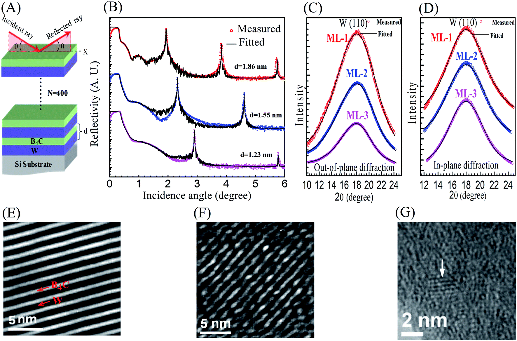 | ||
| Fig. 1 (A) Schematic of the one dimensional periodic W/B4C ML structure with the number of layer pairs N = 400. (B) Measured XRR data and fitted profiles of three MLs at an energy 10 keV. Measured and fitted GIXRD profiles of W (110) diffraction of three MLs at an energy of 17.295 keV in out-of-plane (C) and in in-plane (D) directions. (E) HRTEM image of ML-2. (F) HRTEM image of ML-3. (G) HRTEM image of W layer of ML-2 showing discrete embedded lattice fringe indicated by the arrow in the amorphous matrix. | ||
| Sample no. | d (±0.01) (nm) | W layer | B4C layer | ||||
|---|---|---|---|---|---|---|---|
| t (nm) | σB4C-on-W (±0.03) (nm) | ρ (±0.05) (g cm−3) | t (nm) | σW-on-B4C (±0.03) (nm) | ρ (g cm−3) | ||
| ML-1 | 1.86 | 0.94 | 0.33 | 16.8 | 0.92 | 0.21 | 3.2 (±0.03) |
| ML-2 | 1.55 | 0.99 | 0.37 | 16.8 | 0.56 | 0.20 | 3.7 (±0.03) |
| ML-3 | 1.23 | 0.90 | 0.43 | 16.0 | 0.33 | 0.21 | 9.5 (±0.06) |
To correlate the observed low σ with the structure of layers, a quantitative analysis of crystallinities in layers are done both out-of-plane and in-plane orientations for three MLs using GIXRD (Fig. 1(C and D)). In Table 2, the observed peak positions in MLs are within 17.98–18.10°, which are lower than the stress free bulk W (110) value (2θ = 18.44° at E = 17.295 keV).44 Further, in-plane FWHM is smaller than out-of-plane. Importantly, the approximate average crystallite sizes in both in-plane and out-of-plane are in the range of 0.50–0.67 nm, as obtained using the Scherrer equation.45 It is noted that the contribution of measured stress in W-layers in MLs to the broadening of diffraction peak is negligible.46 Also, the measured GIXRD spectra at 15.6 keV determine the approximate average crystallite sizes in out-of-plane direction for W (211) as ∼1 nm range (see the ESI Fig. S2 and S3†). It is noted that, as W (211) peak intensities are very weak and broad, there may be uncertainty determining the exact position of the peak and width, which may result in uncertainty in values of crystallite size. Similarly, GIXRD results indicate that the B4C layers are amorphous, resulting in a smaller σ of B4C than W (Table 1).
| Sample no. | Out-of-plane | In-plane | ||||
|---|---|---|---|---|---|---|
| Peak position (2θ) (°) | FWHM (°) | Crystallite size (nm) | Peak position (2θ) (°) | FWHM (°) | Crystallite size (nm) | |
| ML-1 | 18.06 | 7.54 | 0.50 | 18.07 | 6.40 | 0.58 |
| ML-2 | 18.10 | 6.98 | 0.54 | 18.07 | 6.20 | 0.60 |
| ML-3 | 17.98 | 5.84 | 0.64 | 18.07 | 5.61 | 0.67 |
Using HRTEM image (Fig. 1(E)), a well-defined layered structure with good density contrast is clearly observed in ML-2 with d = 1.55, revealing a near perfect periodicity. However, as d decreases to 1.23 nm (ML-3) by reducing t of B4C to 0.33 nm (Fig. 1(F)), the optical contrast is significantly deteriorated due to the quasi-continuous nature of B4C, where W atoms get embedded into the quasi-continuous region of B4C. The averaged d obtained from the TEM image for ML-2 and ML-3 are d = 1.48 nm and d = 1.23 nm, respectively, matching well with XRR results. Importantly, the amorphous matrix of W layers with embedded lattice fringes of nano-crystallites (sizes ∼1–5 nm) are observed using the HRTEM image (Fig. 1(G)). The grain size measured using GIXRD is smaller than that observed using TEM due to the average information obtained within the volume of the materials accessed by GIXRD.
RSM data (in terms of momentum vector qx and qz) around the Bragg peaks for ML-1 (Fig. 2(A–C)), ML-2 (Fig. 2(D and E)), and ML-3 (Fig. 2(F and G)) reveal that the scattered intensities from the MLs concentrate in the intensity strip of Bragg sheets, centered at 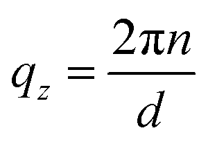 , where
 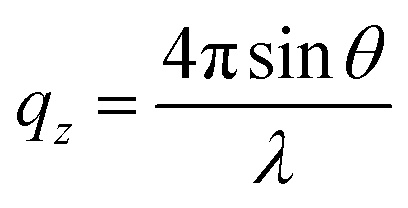 and n is the order of Bragg peak. In Fig. 2, the observation of Bragg sheets evidences vertical periodic structure and provides information on the correlation of interfacial roughness profiles in MLs. In ML-3, the Bragg diffuse scattering is not visible because the intensity is too low. The d of the ML-1, ML-2, and ML-3 is calculated using the separation between two successive observed Bragg sheets Δqz = 3.32 nm−1, 4.1 nm−1, and 5.1 nm−1 as 1.89 nm, 1.53 nm, and 1.23 nm, respectively, which matches well with the XRR result. The ML peaks are extended towards qx (lateral direction) due to resonant diffuse scattering originated by the interference of the waves scattered from the partially correlated interfaces of the ML.47,48 Since the width of the profiles along qx does not change with n, one can conclude that the interface profile is the same for all interfaces. It is noted that the complementary correlated results obtained from different techniques unambiguously ensure an accurate model used with the reliable structural parameters obtained for MLs to describe the exact growth mechanism.
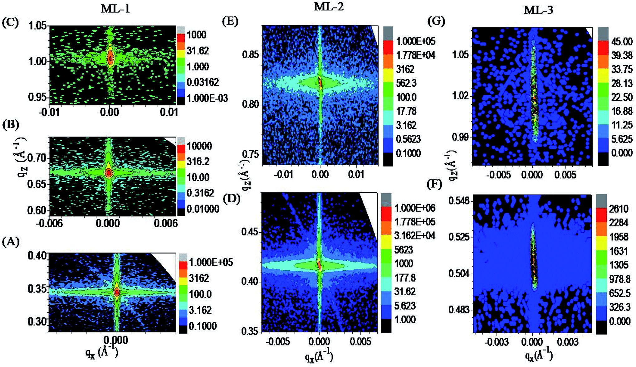 | ||
| Fig. 2 Measured RSM data of three W/B4C ML mirrors at an energy 8.047 keV. The figures in the left panel (A–C) are for ML-1, in the middle panel (D and E) are for ML-2, and in the right panel (F and G) are for ML-3. In the left panel: (A) measure around 1st order, (B) 2nd order, and (C) 3rd order Bragg peaks. Similarly, in the middle: (D) measured at 1st order and (E) 2nd order Bragg peaks. In the right panel: (F) 1st order, and (G) 2nd order peaks. | ||
In addition, total residual stress in ML-1 is compressive, and the value is ∼−0.389 GPa. Similarly, it is also observed that the stress in MLs decreases with increasing N (at fixed d) and with decreasing d (at fixed N) as given in ESI Fig. S4(a and b).† The total stress in the ML film depends on the microstructures of both layers as well as the nature of interfaces.42 Similarly, the lateral uniformity of d over a length of 130 mm was controlled and resulted in variations of about 2.5%. The details are discussed in the ESI Fig. S5.† Further, to corroborate structure–property agreement, hereafter, the results of the measured and predicted optical performances are discussed.
3.2 Optical properties
It is noted that the calibration of such ML mirrors can be carried out at the hard X-ray region, which is very well available in synchrotron facilities. The reflectivities at soft gamma-ray energies can be predicted using extrapolation of known optical constants of materials37,38 and the structural parameters of ML derived from the modeling of hard X-ray data. The optical properties are measured in the hard X-ray region 10–20 keV, for e.g., as shown in Fig. 3(A) for ML-1. At 10 keV, a significantly high reflectivity (≈64%) is measured. As energy increases to 12 keV, reflectivity drops to ∼37% because of the presence of W LII-edge at 11.544 keV. As the energy increases further away from W L-edge, the reflectivity increases. The optical properties of three MLs are compared at a selected energy of 10 keV (Fig. 3(B)), and the results are tabulated in Table 3. Importantly, as the d decreases to 1.23 nm (ML-3), the measured reflectivity catastrophically drops to ∼1% compared to the theoretical value of 62% because of the significant reduction in density contrast (6.5 g cm−3) along with the increase in σ. Also, the non-uniformity of the thickness of the ML structures arises due to the quasi-discontinuity nature of layers, which can also cause the loss of coherence and cause a serious drop of Bragg peak reflectivity. The presence of higher structural imperfection in ML-3 is also clearly observed through a significant decrease in peak intensities multiplied with θ4 by accounting for the approximate 1/θ4 dependency of reflectivity, as shown in the inset of Fig. 3(B). Further, in Table 3, as d decreases, the energy resolving power (E/ΔE) increases due to contributions of larger N to the reflection at higher Bragg angles. It is noted that the measured optical properties in the energy range 10–20 keV are in accordance with the measured structural parameters of MLs. This provides strong support for the argument about the prediction of the reflectivities in the soft gamma-ray region from the structural parameters.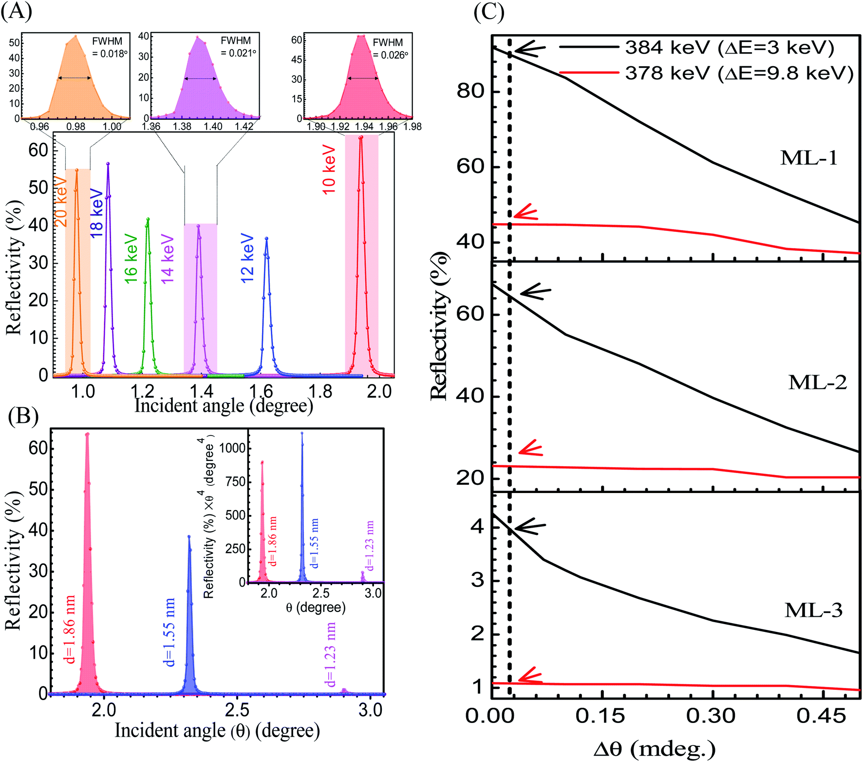 | ||
| Fig. 3 Measured optical properties of ML mirrors in the hard X-ray region (A and B) and calculated in the soft gamma-ray region (C). (A) The bottom figure shows the percent of reflectivity around the 1st order Bragg peak of ML-1 at selected photon energies. The top figures show better clarity of measured angular resolution at three selected energies. (B) Comparative reflectivity (1st order) profiles of three ML mirrors at 10 keV. The inset shows reflectivity multiplied with θ4 as a function of θ. (C) 1st order Bragg peak reflectivity with varying Δθ are calculated at E = 384 keV (ΔE = 3 keV) and 378 keV (ΔE = 9.8 keV). | ||
| Sample no. | d (nm) | Rm (Rth) (%) | E/ΔE |
|---|---|---|---|
| ML-1 | 1.86 | 64 (82) | 76 |
| ML-2 | 1.55 | 39 (73) | 133 |
| ML-3 | 1.23 | 1 (62) | 176 |
It is known25 that the position and amplitude of the 1st order Bragg peak can be accurately predicted at the soft gamma-ray region by wave-optics formalism.34 Fig. 3(C) shows the predicted 1st order peak reflectivities of MLs at two energies E = 384 keV and 378 keV, with the bandwidth of incident photon energy ΔE = 3 keV and 9.8 keV, respectively. It is mentioned that the 1st order peak reflectivity is predicted for three W/B4C MLs at two energies E = 384 keV and 378 keV with the bandwidth of incident photon energy ΔE = 3 keV and 9.8 keV for a comparison with the previously measured reflectivity of WC/SiC based ML optics7 at soft gamma-ray region. The details of the calculation are described in the ESI (Section SI6†). As anticipated, 1st order average peak reflectivity decreases with increasing instrumental angular resolution (Δθ). It is observed that at the marked Δθ = 0.024 milli-degree, the predicted reflectivities are ∼90%, 64%, and 4% for ML-1, ML-2, and ML-3, respectively, for E = 384 keV having ΔE = 3 keV. Whereas, as ΔE increases to 9.8 keV at E = 378 keV, the calculated reflectivities decrease to ∼45%, 23%, and 1% for ML-1, ML-2, and ML-3, respectively. For comparison, at these same photon energies and identical bandwidth, Fernandez-Perea et al.7 evaluated the reflectivity of WC/SiC based ML optics (d = 1.474 nm, N = 300) with an actual beam divergence of 0.024 mdeg. Subsequently, the measured 1st Bragg peak reflectivities are ∼52.6% at E = 384 keV (with ΔE = 3 keV) and ∼23% at E= ∼378 keV (ΔE = 9.8 keV). The difference in reflectivities in both cases is mainly due to the difference in d (d = 1.474 nm earlier, but d = 1.55 nm present). For e.g., if the d = 1.474 nm is kept identical in W/B4C, predicted reflectivities are ∼53% and 17% at E = 384 and 378 keV, respectively, which is comparable with WC/SiC. Thus, an identical percent of peak reflectivity with additional merit of having a superior optical contrast of W/B4C is expected to provide higher photon flux compared to WC/SiC. Here, it is noted that though the comparison of the predicted reflectance of W/B4C with the actually measured reflectance of WC/SiC at soft gamma-ray energies may not be a more accurate way for a direct correlation, the present results provide strong evidence as a candidate of choice for such high energy application.
4. Discussion
The observed desirable structure of ML optics with required stresses is obtained by tailoring the surface density of grains and kinetics of ad-atoms. At the optimized process parameters, W forms more surface density of grains with the mean size of grains of the order of sub-nanometers tending towards amorphous structure (corroborated using GIXRD and well correlated with HRTEM) and relatively compact arrangements of atoms (confirmed using XRR) near the continuous limit. The observed microstructure implies that the growth mechanism favors the formation of many crystalline nuclei rather than the growth of previously formed nuclei at the nucleation/island growth stage. As a result, we obtained an average desirable low interface width down to 0.27 nm (ML-1) required for such optics. A model representing the correlation between the morphology and surface density of grains is shown in Fig. 4.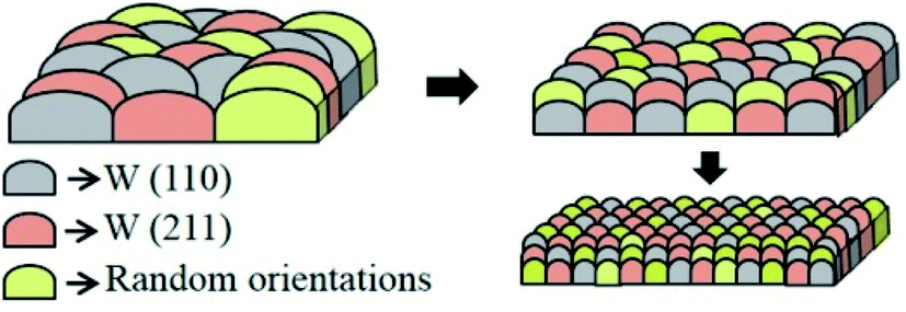 | ||
| Fig. 4 Schematic of the morphology of the W layer near the continuous limit. As the surface density of grains increases gradually (indicated by arrows) towards the average size of sub-nanograins, the morphology tends toward more compact and smoother. The color code represents the different orientations of crystallites. | ||
Regarding density contrast (Table 1), the observed lower and higher values of densities of W layers and the B4C layers, respectively, than their corresponding bulk values (19.3 g cm−3 and 2.52 g cm−3 for W and B4C, respectively) may be due to the expected diffusion of B4C molecules into W layer and vice versa would produce such effect at the ultra-low thickness, which is clearly observed using TEM. In addition to diffusion, due to a thermally mediated event, atoms/molecules could get there by plantation during the sputtering process. In ML-3, as the t of B4C layers decreases to 0.33 nm, it forms quasi-continuous layers, where more W atoms get embedded (using HRTEM). As a result, a significant increase of ρ of B4C layer (∼3.77 times the bulk value) is observed (Table 1). This reduces the density contrast, and hence reflectivity decreases drastically to ∼1%. It is noteworthy to mention that for ML, particularly with d = 1.23 nm (ML-3), instead of keeping a very small thickness of B4C layers (0.33 nm), the gamma value (ratio of high-Z layer thickness to period thickness) of ML could be slightly decreased by optimizing the tolerable amount of the extent of quasi-continuity in both W and B4C layers to obtain a comparable further better structure. The observed density contrast (ρW − ρB4C) is 13.6 g cm−3 and 13.1 g cm−3 for ML-1 and ML-2, respectively. It is noted that earlier in the case of the WC/SiC ML mirror,7 the density difference was taken as 12.82 g cm−3, which was accounted for by considering the bulk density for the WC layer (15.8 g cm−3) and density of a reasonable thicker film for the SiC layer (2.98 g cm−3). Generally, at an ultra-low thickness of the layers, the actual density of layers in the ML stack may be lower than the bulk value. This indicates that W/B4C is an optically better material system with higher density contrast.
The observed small and dense crystallites of W lead to compressive stress in W layers. But, the observed lattice period in the W layer is greater than the bulk values. Similar observations were also reported earlier,49 and were explained using the atomic peening model.50 Atomic peening arises due to bombardment of the grown W layers by energetic species, such as Ar neutrals and sputtered atoms/molecules during growth. The energetic particles increase the mobility of the surface atoms required for densification. Further, atomic peening causes atoms to be incorporated in the growing films, as a result of which they fill vacancies trapped inside the film during growth, which leads to denser films. In addition, atomic peening may cause the formation of interstitials as its energy of formation is not so high compared with the atomic bombardment energies encountered in the sputtering processes. The formation of interstitials may cause the lattice period to be larger than the bulk. Again, the measured values of total compressive stress in W/B4C MLs with N = 400 in the present study are comparable to that of earlier reported stress for WC/SiC ML optics.31 Due to the well-defined structure in ML-1 and ML-2, significantly high optical properties are measured in the hard X-ray region (10–20 keV) as well as the predicted high peak reflectivities in the soft gamma-ray region. The measured structure–property of MLs is well correlated. Thus, all the above results strongly support that the W/B4C system would be an efficient mirror for soft gamma-rays.
5. Conclusions
In conclusion, we demonstrated metal based (W/B4C) high efficiency ML optics for high energy applications. The experimental evidence indicates that near the layer continuous limit, metal (W) in ML structure forms average sub-nanometer grains approaching amorphous structure by tailoring the surface density of grains. This ensures concurrently the lowest desirable σ = 0.27 nm, low stress (−389 MPa), and high density contrast (13.6 g cm−3) in ML structure (for e.g., ML with d = 1.86 nm and N = 400), desirable for such optics. The good agreement between measured and predicted hard X-ray optical properties as well as predicted soft gamma-ray reflectivities, makes a strong case supporting W/B4C as one of the prospective materials of choice for such optics. The present approach could open up a path for progress in the understanding of nano-scale layered structure materials as well as have a wide impact on the developed ML optics for technological implications in the frontier research areas of soft gamma-ray spectroscopy.Abbreviations
| ML | Multilayer |
| DC | Direct current |
| RF | Radio frequency |
| XOP | X-ray oriented program |
| XRR | X-ray reflectivity |
| RSM | Reciprocal space mapping |
| TEM | Transmission electron microscopy |
| HRTEM | High resolution transmission electron microscopy |
| GIXRD | Grazing incidence X-ray diffraction |
Author contributions
M. N. conceived the idea. A. M. and M. N. fabricated the samples. A. M., P. C. P. and M. N. performed hard XRR measurements. S. J., D. V. U. and A. M. carried out stress measurements and analysis using interferometer. A. G., A. M., V. R. R., and M. N. performed RSM measurements along with U. P. who played a key role providing detailed technical planning for the RSM measurements, and spectral interpretations. A. M., M. N., M. N. S. and A. K. S. performed GIXRD measurements. A. M., H. S., M. N. and A. K. S. carried out TEM measurements. A. M. and M. N. compiled all the measured data. All the authors discussed the results in preparing the scientific contents of the manuscript. M. N. and A. M. wrote the manuscript. All authors reviewed the manuscript.Conflicts of interest
There are no conflicts of interest to declare.Acknowledgements
The authors gratefully thank BL16 beamline technical staff of Indus-2 SR facility for their support during the XRR measurements. We sincerely acknowledge M. K. Tiwari for helpful scientific discussion on XRR results.References
- H. Mimura, S. Handa, T. Kimura, H. Yumoto, D. Yamakawa, H. Yokoyama, S. Matsuyama, K. Inagaki, K. Yamamura, Y. Sano, K. Tamasaku, Y. Nishino, M. Yabashi, T. Ishikawa and K. Yamauchi, Nat. Phys., 2010, 6, 122–125 Search PubMed.
- M. Zhao, Y. Ye, Y. Han, Y. Xia, H. Zhu, S. Wang, Y. Wang, D. A. Muller and X. Zhang, Nat. Nanotechnol., 2016, 11, 954–959 CrossRef CAS PubMed.
- E. Benckiser, M. W. Haverkort, S. Bruck, E. Goering, S. Macke, A. Frano, X. Yang, O. K. Andersen, G. Cristani, H.-U. Habermeier, A. V. Boris, I. Zegkinoglou, P. Wochner, H.-J. Kim, V. Hinkov and B. Keimer, Nat. Mater., 2011, 10, 189–193 CrossRef CAS PubMed.
- N. Nakagawa, H. Y. Hwang and D. A. Muller, Nat. Mater., 2006, 5, 204–209 CrossRef CAS.
- A. Gozar, G. Logvenov, L. F. Kourkoutis, A. T. Bollonger, L. A. Giannuzzi, D. A. Muller and I. Bozovic, Nature, 2008, 455, 782–785 CrossRef CAS PubMed.
- W. Kuch, L. I. Chelaru, F. Offi, J. Wang, M. Kotsugi and J. Kirschner, Nat. Mater., 2006, 5, 128–133 CrossRef CAS PubMed.
- M. Fernandez-Perea, M. A. Descalle, R. Soufli, K. P. Ziock, J. Alameda, S. L. Baker, T. J. McCaville, V. Honkimaki, E. Ziegler, A. C. Jakobsen, F. E. Christensen and M. J. Pivovaroff, Phys. Rev. Lett., 2013, 111, 027404 CrossRef PubMed.
- J. Ruz, N. F. Brejnholt, J. B. Alameda, T. A. Decker, M. A. Descalle, M. Fernandez-Perea, R. M. Hill, R. A. Kisner, A. M. Melin, B. W. Patton, R. Soufli, K. Jiock and M. J. Pivovaroff, Nucl. Instrum. Methods Phys. Res., Sect. A, 2015, 777, 15–19 CrossRef CAS.
- F. A. Harrison, et al., Astrophys. J., 2013, 770, 103 CrossRef.
- B. W. Grefenstette, et al., Nature, 2014, 506, 339 CrossRef CAS PubMed.
- A. Haase, V. Soltwisch, S. Braun, C. Laubis and F. Scholze, Opt. Express, 2017, 25, 15441–15455 CrossRef CAS PubMed.
- D. L. Windt, S. Donguy, C. J. Hailey, J. Koglin, V. Honkimaki, E. Ziegler, F. E. Christensen, H. Chen, F. A. Harrison and W. W. Craig, Appl. Opt., 2003, 42, 2415–2421 CrossRef CAS PubMed.
- A. F. Jankowski, L. R. Schrawyer, M. A. Wall, W. W. Craig, R. I. Morales and D. M. Makowiecki, J. Vac. Sci. Technol., A, 1989, 7, 2914–2918 CrossRef CAS.
- M. A. MacDonald, F. Schafers and A. Gaupp, Opt. Express, 2009, 17, 23290–23298 CrossRef CAS PubMed.
- D. L. Windt, E. M. Gullikson and C. C. Walton, Opt. Lett., 2002, 27, 2212–2214 CrossRef CAS PubMed.
- M. S. Bibishkin, N. I. Chkhalo, A. A. Fraerman, A. E. Pestov, K. A. Prokhorov, N. N. Salashchenko and Y. A. Vainer, Nucl. Instrum. Methods Phys. Res., Sect. A, 2005, 543, 333–339 CrossRef CAS.
- C. C. Walton, G. Thomas and J. B. Kortright, Acta Mater., 1998, 46, 3767 CrossRef CAS.
- D. L. Windt, SPIE Proc., 2007, vol. 6688, p. 66880R Search PubMed.
- N. Ghafoor, F. Erikson, E. Gullikson, L. Hultman and J. Birch, Appl. Phys. Lett., 2008, 92, 091913 CrossRef.
- P. Naujok, S. Yulin, A. Bianco, N. Mahne, N. Kaiser and A. Tunnermann, Opt. Express, 2015, 23, 4289 CrossRef CAS PubMed.
- J. Peng, W. Li, Q. Huang and Z. Wang, Sci. Rep., 2016, 6, 31522 CrossRef CAS PubMed.
- B. Girault, P. Villain, E. Pe. Bourhis and P. Goudeau, Surf. Coat. Technol., 2006, 201, 4372–4376 CrossRef CAS.
- D. L. Windt, F. E. Christensen, W. W. Craig, C. Hailey, F. A. Harrison, M. Jimenez-Garate, R. Kalyanaraman and P. H. Mao, J. Appl. Phys., 2000, 88, 460–470 CrossRef CAS.
- D. L. Windt, F. Christensen, W. Craig, C. Hailey, F. Harrison, M. Jimenez-Garate, R. Kalyanaraman and P. Mao, SPIE Proc., 2000, vol. 4012, pp. 442–447 Search PubMed.
- M. J. Pivovaroff, K. P. Ziock, M. Fernandez-Perea, M. J. Harrison and R. Soufli, Nucl. Instrum. Methods Phys. Res., Sect. A, 2014, 743, 109–113 CrossRef CAS.
- C. P. Jensen, K. K. Madsen and F. E. Christensen, Exp. Astron., 2005, 20, 93–103 CrossRef.
- T.-W. Huang, H.-Y. Lee, Y.-W. Hsieh and C.-H. Lee, J. Cryst. Growth, 2002, 237–239, 492–495 CrossRef CAS.
- P. C. Pradhan, D. Gangir, A. Majhi, M. Nayak, A. Biswas, D. Bhattacharyya and G. S. Lodha, J. Phys. D: Appl. Phys., 2016, 49, 135305 CrossRef.
- P. C. Pradhan, A. Majhi, M. Nayak, M. Nand, P. Rajput, D. K. Shukla, A. Biswas, S. K. Rai, S. N. Jha, D. Bhattacharyya, D. M. Phase and N. K. Sahoo, J. Appl. Phys., 2016, 120, 045308 CrossRef.
- Y. A. Vainer, A. E. Pestov, K. A. Prokhorov, N. N. Salashchenko, A. A. Fraerman, V. V. Chernov and N. I. Chkhalo, J. Exp. Theor. Phys., 2006, 103, 346–353 CrossRef CAS.
- M. Fernandez-Perea, M. J. Pivovaroff, R. Soufli, J. Alameda, P. Mirkarimi, M. A. Descalle, S. L. Baker, T. McCarville, K. Ziock, D. Hornback, S. Romaine, R. Bruni, Z. Zhong, V. Honkimaki, E. Ziegler, F. E. Christensen and A. C. Jakobsen, Nucl. Instrum. Methods Phys. Res., Sect. A, 2013, 710, 114–119 CrossRef CAS.
- M. Nayak, P. N. Rao and G. S. Lodha, Asian J. Phys., 2010, 19, 287–300 Search PubMed.
- G. Das, S. R. Kane, A. Khooha, A. Singh and M. K. Tiwari, Rev. Sci. Instrum., 2015, 86, 055102 CrossRef PubMed.
- D. L. Windt, IMD Version 5.0, 2013, seehttp://www.rxollc.com/idl/index.html Search PubMed.
- M. Born, and E. Wolf, Principles of Optics, Pergamon Press, Oxford, UK, 6th edn, 1980 Search PubMed.
- D. G. Stearns, J. Appl. Phys., 1989, 65, 491–506 CrossRef CAS.
- C. T. Chantler, J. Phys. Chem. Ref. Data, 1995, 24, 71–643 CrossRef CAS.
- C. T. Chantler, J. Phys. Chem. Ref. Data, 2000, 29, 597–1048 CrossRef CAS.
- B. L. Henke, E. M. Gullikson and J. C. Davis, At. Data Nucl. Data Tables, 1993, 54, 181–342 CrossRef CAS , see http://henke.lbl.gov/optical_constants/.
- A. K. Sinha, A. Sagdeo, P. Gupta, A. Upadhyay, A. Kumar, M. N. Singh, R. K. Gupta, S. R. Kane, A. Verma and S. K. Deb, J. Phys.: Conf. Ser., 2013, 425, 072017 CrossRef CAS.
- K. D. Rao, D. V. Udupa, C. Prathap, A. Rathod, R. Balasubramaniam and N. K. Sahoo, Opt Laser. Eng., 2015, 66, 204–209 CrossRef.
- A. Majhi, P. C. Pradhan, S. Jena, M. N. Singh, M. Nayak, S. K. Rai and D. V. Udupa, J. Appl. Crystallogr., 2019, 52, 332–343 CrossRef CAS.
- P. C. Pradhan, A. Majhi and M. Nayak, J. Appl. Phys., 2018, 123, 095302 CrossRef.
- M. C. Morris, H. F. McMurdie, E. H. Evans, B. Paretzkin, J. H. De. Groot, B. S. Weeks, R. J. Newberry, C. R. Hubbard, and S. J. Carmel, Standard X-Ray Diffraction Powder Patterns Section-15, U.S. Government Printing Office, Washington, 1978 Search PubMed.
- B. D. Cullity, Elements of X-Ray Diffraction; Addition-Wesley Publishing Company, Massachusetts, 1956 Search PubMed.
- A. Majhi, M. Dilliwar, P. C. Pradhan, S. Jena, M. Nayak, M. N. Singh, D. V. Udupa and N. K. Sahoo, J. Appl. Phys., 2018, 124, 115306 CrossRef.
- V. Holy and T. Baumbach, Phys. Rev. B: Condens. Matter Mater. Phys., 1994, 49, 10668–10676 CrossRef CAS PubMed.
- U. Pietsch, V. Holý, and T. Baumbach, High-Resolution X-ray Scattering From Thin Films to Lateral Nanostructures, Springer-Verlag, 2004 Search PubMed.
- P. Villain, P. Goudeau, J. Ligot, S. Benayoun, K. F. Badawi and J. J. Hantzpergue, J. Vac. Sci. Technol., A, 2003, 21, 967–972 CrossRef CAS.
- F. M. D'Heurle and J. M. E. Harper, Thin Solid Films, 1989, 171, 81–92 CrossRef.
Footnote |
| † Electronic supplementary information (ESI) available. See DOI: 10.1039/d1ra04412e |
| This journal is © The Royal Society of Chemistry 2021 |