
 Open Access Article
 This Open Access Article is licensed under a Creative Commons Attribution-Non Commercial 3.0 Unported Licence
Tuning the charge carrier mobility in few-layer PtSe2 films by Se![[thin space (1/6-em)]](https://www.rsc.org/images/entities/h2_char_2009.gif) :Pt ratio
:Pt ratio
Jana Hrdá ab,
Valéria Taškováa,
Tatiana Vojtekováac,
Lenka Pribusová Slušnáa,
Edmund Dobročkaa,
Igor Píšd,
Federica Bondinod,
Martin Hulmana and
Michaela Sojková*a
ab,
Valéria Taškováa,
Tatiana Vojtekováac,
Lenka Pribusová Slušnáa,
Edmund Dobročkaa,
Igor Píšd,
Federica Bondinod,
Martin Hulmana and
Michaela Sojková*a
aInstitute of Electrical Engineering, SAS, Dúbravská cesta 9, 841 04 Bratislava, Slovakia. E-mail: michaela.sojkova@savba.sk
bFaculty of Electrical Engineering and Information Technology, Slovak University of Technology, Ilkovičova 3, 812 09 Bratislava, Slovakia
cFaculty of Mathematics, Physics and Informatics, Comenius University in Bratislava, Mlynská dolina F2, 842 48, Bratislava, Slovak Republic
dIOM-CNR, Laboratorio TASC, S.S. 14 km 163.5, 34149 Basovizza, Trieste, Italy
First published on 10th August 2021
Abstract
Recently, few-layer PtSe2 films have attracted significant attention due to their properties and promising applications in high-speed electronics, spintronics and optoelectronics. Until now, the transport properties of this material have not reached the theoretically predicted values, especially with regard to carrier mobility. In addition, it is not yet known which growth parameters (if any) can experimentally affect the carrier mobility value. This work presents the fabrication of horizontally aligned PtSe2 films using one-zone selenization of pre-deposited platinum layers. We have identified the Se![[thin space (1/6-em)]](https://www.rsc.org/images/entities/char_2009.gif) :Pt ratio as a parameter controlling the charge carrier mobility in the thin films. The mobility increases more than twice as the ratio changes in a narrow interval around a value of 2. A simultaneous reduction of the carrier concentration suggests that ionized impurity scattering is responsible for the observed mobility behaviour. This significant finding may help to better understand the transport properties of few-layer PtSe2 films.
:Pt ratio as a parameter controlling the charge carrier mobility in the thin films. The mobility increases more than twice as the ratio changes in a narrow interval around a value of 2. A simultaneous reduction of the carrier concentration suggests that ionized impurity scattering is responsible for the observed mobility behaviour. This significant finding may help to better understand the transport properties of few-layer PtSe2 films.
Any material used in high-speed electronics needs to fulfil basic requirements, including a high current on/off switch ratio and high charge carrier mobility for fast operation.1 Layered 2D transition metal dichalcogenide (TMDC) materials with tuneable band gap and transitional behaviour have considerable potential in this area.2 TMDCs contain over 40 combinations of transition metal and chalcogenides.3 Platinum diselenide (PtSe2) belongs to a group of noble-TMDCs, which naturally occurs in the 1T phase.4 PtSe2 has been predicted as an exceptional material, and in addition, experiments proved its outstanding properties, such as widely tuneable band gap, air stability and high carrier mobility. Single-layer to few-layer PtSe2 is a p-type semiconductor, thicker or bulk PtSe2 shows a semi-metallic character.5,6 It has been confirmed, that PtSe2 also has optoelectronic performance7 and photocatalytic activities.5,6 This extends its possible applications in photodetection8 or quick-response gas sensing.9,10 Avsar et al.11 showed that atomic-scale defects could transform non-magnetic 2D crystals into magnetic phases. Using first-principles calculations they suggest that a platinum vacancy defect yields antiferro- (ferro-) magnetic ordering in mono- (bi-) layer PtSe2. For all the applications mentioned above, high quality and large-area PtSe2 films are necessary.
Several possible fabrication methods of monolayer and few-layer PtSe2 have been developed. Yan et al. used molecular beam epitaxy to create high-quality epitaxial thin PtSe2 films with a controllable thickness.12 This method is outstanding for creating large-size single-crystalline films on various substrates. On the other hand, this method is less suitable for large-scale device fabrication. Chemical vapour deposition13,14 and direct selenization of thin platinum films (also called thermally assisted conversion-TAC)6,15 are extensively used to fabricate PtSe2 films on the nanometres thickness range. This method is suitable for preparing large-area films. However, nanocrystals are oriented randomly, yet no long-range ordering within the layer has been experimentally achieved. This is one of the limiting factors for much lower charge carrier mobility than it was predicted.
As we have already mentioned above, PtSe2 is a promising material for application in electronics. The charge carrier mobility of PtSe2 has been predicted to be one of the highest among TMDCs.16 However, the experimentally measured carrier mobility of PtSe2 is much lower than the theoretically predicted value.2 The mobility strongly depends on the scattering phenomena within the material. Intrinsic mobility is determined by scattering caused by lattice vibrations.1 For 2D materials in general, several factors including charge impurity, structural defects or surface optical phonons scattering, dominate the charge transport.17,18 For example, point defects typically lower the carrier mobility or degrade mechanical properties of 2D materials.19 Fabrication method also strongly influences the film quality as well as charge carrier mobility values. The highest values were obtained on PtSe2 flakes peeled off from bulk crystals using a scotch tape-based mechanical exfoliation. Zhao et al.16 fabricated a few-layer device on SiO2/Si substrate exhibiting a semiconducting behaviour with high room-temperature electron mobility (210 cm2 V−1 s−1) in a back-gated configuration. Xu et al.20 demonstrated the controllable doping in PtSe2 few-layer films prepared by selenization. Depending on the growth conditions, they fabricated both n-type and p-type PtSe2 films of various thicknesses.20 The films showed FET mobility of 14 and 15 cm2 V−1 s−1 for p-type and n-type FETs, respectively. Selenization of pre-deposited platinum layers leads to PtSe2 films exhibiting p-type semiconducting behaviour with hole mobility values up to 13 cm2 V−1 s−1.21 However, after the fabrication of FET structure, the field effect mobility decrease to 0.3 cm2 V−1 s−1.
This paper presents the fabrication of few-layer PtSe2 films by one-zone selenization of a pre-deposited platinum layer. We studied how nitrogen flow during the selenization process affects the chemical composition, structural, and electrical transport properties of the final PtSe2 films. In contrast, the temperature, heating rate, selenization time, and initial thickness of Pt pre-deposited layers were constant. To analyse the structural and chemical properties of prepared PtSe2 films we used the combination of X-ray photoelectron spectroscopy (XPS), X-ray diffraction (XRD) and Raman spectroscopy. The charge carrier mobility of the samples was determined from the Hall-effect measurement. We found a correlation between the selenium concentration in the sample and its carrier mobility. The charge carrier mobility values scale linearly with Se:Pt ratio close to 2.
Experimental
PtSe2 fabrication
PtSe2 thin films were prepared by a two-step method on the top of the c-plane (0001) sapphire substrate. The substrate dimensions were 10 × 10 mm2. At first, Pt films were prepared using DC magnetron sputtering in Ar atmosphere (10−3 mbar) from a platinum target at room temperature. The DC power and emission current were set to 580 W and 0.18 A, respectively. The thickness of the as-prepared Pt films was set by the rotation speed of a sample holder. Further, the pre-deposited Pt layers were selenized in a custom-designed CVD chamber.22 The substrate and Se powder are placed in the same position in the center of the furnace. The temperature of the substrate and powder is the same during the growth.23,24 This is in contrast to the standard CVD method, where the reaction takes place in a two-zone furnace with selenium powder and Pt substrate heated at different temperatures. Annealing temperature (550 °C), annealing time (30 min) and heating rate (25 °C min−1) stay unchanged while the nitrogen flow rate ranged from 20 to 350 sccm.Characterization
Results and discussion
A series of PtSe2 few-layer films were prepared using selenization of 1 nm thick platinum layer on a c-plane sapphire substrate. Annealing temperature, time, and heating rate were similar for all experiments while the nitrogen flow rate varied from 20 up to 350 sccm. The crystal structure of as-prepared PtSe2 films was determined by XRD measurements in a symmetrical θ/2θ configuration (Fig. 1(a)). Only a 001 diffraction of the hexagonal 1T PtSe2 phase was visible in the pattern, meaning the layers are aligned horizontally with the c-axis perpendicular to the substrate. The presence of the Laue oscillations on both sides of the dominant 001 diffraction proves the high crystallinity and homogenous thickness of the films. There was no significant difference between patterns using various N2 flow rates. The thickness of as-prepared films was calculated from Laue oscillations and from X-ray reflectivity measurements (Fig. 1(b)) using DIFFRAC.LEPTOS software.22 All the films have a similar thickness (4 ± 0.5 nm) corresponding to 8 ± 1 monolayers of PtSe2.28 Azimuthal (φ-scan) measurements of 101 diffraction of PtSe2 and 104 diffraction of sapphire revealed the in-plane crystallographic orientation of the films (Fig. 1(c)). The presence of recognizable maxima indicates that the layers tend to grow epitaxially. However, the maxima are broad suggesting that the in-plane disorder is still present in the sample. Compared with our previous work,22 peaks have relatively low intensity due to the small sample thickness. The orientation of the layers on the substrate reflects the relative position of the diffraction maxima in the φ-scans of sapphire (black curve in Fig. 1(b)) and PtSe2. From these positions, we can conclude that the hexagonal lattice of PtSe2 is rotated by 30° with respect to the substrate lattice.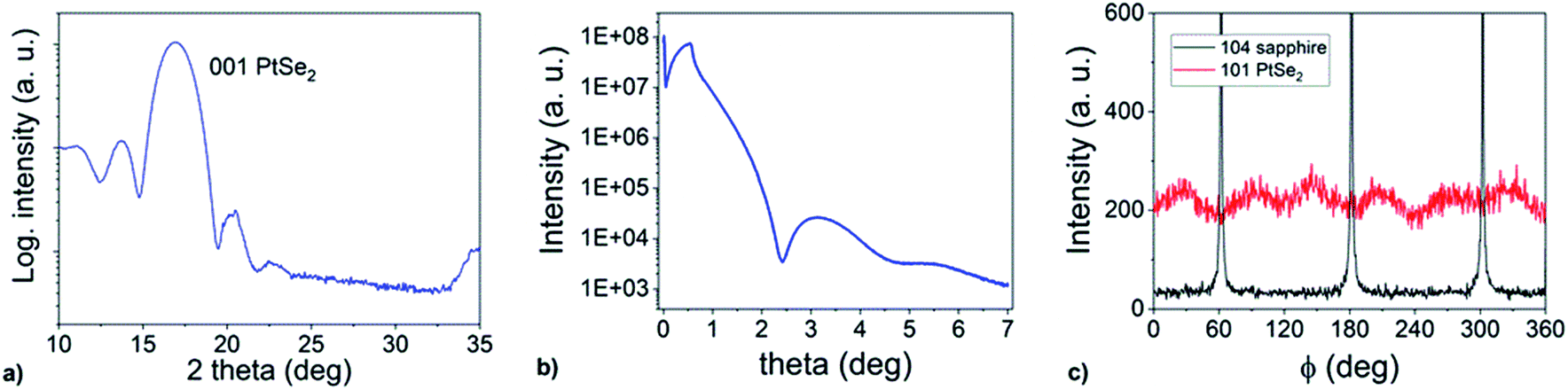 | ||
| Fig. 1 (a) Typical XRD pattern of PtSe2 film prepared by selenization of 1 nm thick Pt layer at 550 °C during 30 min. (b) Typical XRR spectra of PtSe2 film prepared by selenization of 1 nm thick Pt layer at 550 °C during 30 min. (c) Corresponding φ-scan of 101 diffraction of PtSe2 and 104 diffraction of sapphire. | ||
Fig. 2 shows Raman spectra of PtSe2 films prepared at 550 °C/30 min using different nitrogen flow rates. The vibration modes belonging to PtSe2 are visible in spectra, concretely Eg mode, which occurs at around 175 cm−1 and the A1g mode at approximately 207 cm−1. The spectra are normalized to the Eg line intensity. The A1g/Eg intensity ratio increases as the number of PtSe2 layers increases.29 Since no systematic changes were observed in the A1g/Eg ratio, the nitrogen flow rate does not have any noticeable impact on the thickness of the resulting PtSe2 films. The broad and less intense band at around 230 cm−1 is assigned to an overlap between two longitudinal optical modes.29 The shape of the band reflects the thickness of the PtSe2 layer and does not change with the nitrogen flow, confirming the conclusion drawn from the A1g/Eg intensity ratio.
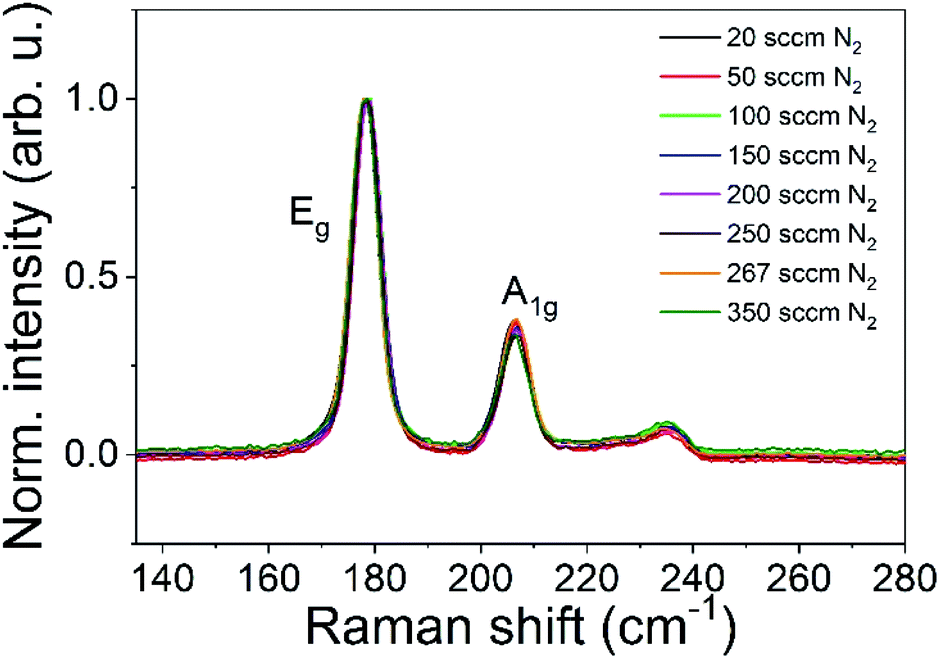 | ||
| Fig. 2 Normalized Raman spectra of PtSe2 films prepared by selenization of 1 nm thick Pt layer at 550 °C during 30 min with different nitrogen flow rates. | ||
The electrical measurements were performed on as-prepared films without patterning. The indium contacts were cold pressed into the corners of a sample. The Hall coefficient and the resistivity of the PtSe2 samples were measured by the van der Pauw (vdP) method. At first, conductivity (σ) measurements were performed in vdP configuration. From the measurements in the magnetic field, we estimated the Hall coefficient RH and charge carrier concentration. The charge carrier mobility μH was afterwards calculated from these quantities as μH = (RH × σ). The polarity of Hall the coefficient determines the type of conductivity. For all as-prepared PtSe2 films showed p-type conductivity. The calculated charge carrier mobility values range from 10.8 to 27.1 cm2 V−1 s−1 (Table 1) for the films prepared with different N2 flow rates.
| Nitrogen flow rate (sccm) | Hall mobility μ (cm2 V−1 s−1) | Concentration of charge carriers (cm−2) | Hall constant (cm2/As) | Se:Pt ratio (1200 eV) |
|---|---|---|---|---|
| 20 | 20.3 | 1.1884 × 10¹⁴ | 5.2522 × 10⁴ | 2 |
| 50 | 14 | 1.7468 × 10¹⁴ | 3.5731 × 10⁴ | 1.971 |
| 100 | 15.4 | 1.4144 × 10¹⁴ | 4.4130 × 10⁴ | 1.979 |
| 150 | 23.19 | 8.30 × 10¹³ | 7.50 × 10⁴ | 2.002 |
| 200 | 18.1 | 1.4761 × 10¹⁴ | 4.2283 × 10⁴ | 1.988 |
| 250 | 27.1 | 1.0739 × 10¹⁴ | 5.8122 × 10⁴ | 2.035 |
| 267 | 24.4 | 6.72 × 10¹³ | 9.29 × 10⁴ | 2.015 |
| 350 | 10.8 | 3.5220 × 10¹⁴ | 1.7722 × 10⁴ | 1.971 |
Results from the Hall measurements listed in Table 1 show no clear correlation between the nitrogen flow rate and carrier mobility. Next, we performed synchrotron-radiation XPS measurements with a photon energy of 1200 eV to estimate the films' chemical composition. Fig. 3 shows typical Pt 4f and Se 3d spectra of the films prepared at 550 °C/30 min. The binding energies of the main peaks, 73.07 ± 0.05 eV for Pt 4f7/2 and 54.40 ± 0.03 eV for Se 3d5/2, are in good agreement with the reported values for PtSe2.29,30 We found the Se:Pt ratio to be 2.1 ± 0.2. To reduce the uncertainty originating from the cross-sections,27,31 the Se:Pt atomic ratios were re-scaled to the value obtained for the sample prepared at the lowest nitrogen flow rate. The calculated values are shown in Table 1.
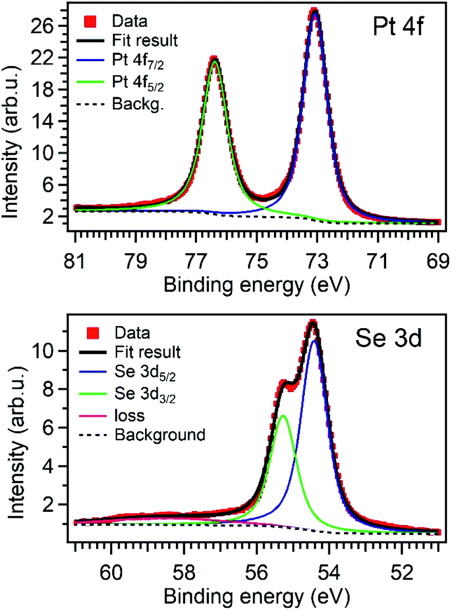 | ||
| Fig. 3 Typical XPS spectra of PtSe2 films prepared by selenization of 1 nm thick Pt layer at 550 °C during 30 min. | ||
We can see from the table that the charge carrier mobility values are different for different Se:Pt ratio. Xu et al.20 studied the influence of the growth parameters on the electronic properties of PtSe2 films. They showed that the slow cool-down process with a continuous supply of Se precursor enables a complete (over) selenization. Se vacancies can be filled at high temperature in such a process, which resulted in p-type mobility with Se:Pt ratio of about 2.45. On the other hand, the selenization process ends quickly for rapid cooling as the temperature rapidly drops down. For this process, they obtained n-type PtSe2 with Se:Pt ratio of about 1.96. However, the field effect mobility values were almost the same for both types of the films (14 and 15 cm2 V−1 s−1 for p-type and n-type FETs, respectively). In contrast, the use of the different N2 flow rates did not significantly change the Se:Pt as in the above-mentioned method. For our films, Se:Pt ranged from 1.97 to 2.03. In all the samples presented here, holes are dominating charge carriers.
When we analysed the values of the charge carrier mobility, Se:Pt ratio and the N2 flow rate, no convincing dependence can be deduced from Table 1. However, we found a correlation between Se:Pt ratio and the charge carrier mobility and charge carrier concentration. Fig. 4 demonstrates the dependence of carrier mobility and concentration on the Se:Pt ratio. The mobility had increased more than twice when Se:Pt increased in a relatively narrow range from 1.97 to 2.03. In contrast, the charge carrier concentration decreases as the Se:Pt is growing. Thus, mobility increases when the carrier concentration gets reduced. Such mobility vs. concentration relationship is due to the scattering of mobile charge carriers on ionized impurities. The smaller the concentration, the larger the scattering time and, consequently, carrier mobility.32
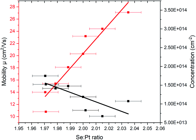 | ||
| Fig. 4 Se:Pt ratio vs. charge carrier mobility and carrier concentration of PtSe2 films prepared by selenization of 1 nm thick Pt layer at 550 °C during 30 min with different N2 flow rate. The solid lines are a linear fits to the experimental values. Error bars represent uncertainty in XPS peak background removal. | ||
Conclusions
In conclusion, we report on the chemical, structural and electrical transport properties of few-layer PtSe2 films grown on a c-plane sapphire substrate using selenization of pre-deposited platinum layers. The nitrogen flow rate was the only parameter changed during PtSe2 growth. Other parameters such as Pt thickness, heating rate, annealing temperature, and process time, stayed unchanged. The structural characteristics and the thickness of the films show no sensitivity to the nitrogen flow rate. Similarly, the charge carrier mobility also reveals no convincing dependence on the flow rate, although it ranges from 10.8 up to 27.1 cm2 V−1 s−1. On the other hand, we found a clear correlation between carrier mobility and Se:Pt ratio in the films. The charge carrier mobility increases with increasing Se:Pt ratio. At the same time, the carrier concentration decreases, meaning the ionized impurity scattering is likely responsible for the observed mobility vs. Se:Pt dependence. We may conclude that even though the nitrogen flow rate does not appear to control the structural and transport properties of as-grown films directly, we have identified the Se:Pt ratio as a parameter that controls the charge carrier mobility.
Author contributions
MS, JH and VT performed the experimental syntheses and characterizations of PtSe2 layers; ED performed the XRD measurements and interpretation of the results; TV and LPS performed the Raman characterization; IP and FB performed the XPS measurements and interpretation of the results; MS, JH and VT performed electrical measurements; JH and MS supervised the project and wrote the manuscript. All authors discussed the results and commented on the manuscript.Conflicts of interest
There are no conflicts to declare.Acknowledgements
This work was supported by the Slovak Research and Development Agency, APVV-17-0352, APVV-17-0560, APVV-19-0365 and Slovak Grant Agency for Science VEGA 2/0059/21. XPS measurements carried out at BACH beamline of CNR at Elettra synchrotron facility in Trieste (Italy) were performed thanks to the mobility project CNR-SAV-20-03. This study was performed during the implementation of the project Building-up Centre for advanced materials application of the Slovak Academy of Sciences, ITMS project code 313021T081 supported by Research & Innovation Operational Programme funded by the ERDF. We acknowledge Ján Dérer for the deposition of platinum films. I. P. and F. B. acknowledge funding from EUROFEL project (RoadMap Esfri).Notes and references
- S. H. Mir, V. K. Yadav and J. K. Singh, ACS Omega, 2020, 5, 14203–14211 CrossRef CAS.
- Y. Gong, Z. Lin, Y.-X. Chen, Q. Khan, C. Wang, B. Zhang, G. Nie, N. Xie and D. Li, Nano-Micro Lett., 2020, 12, 174 CrossRef CAS.
- M. Chhowalla, H. S. Shin, G. Eda, L.-J. Li, K. P. Loh and H. Zhang, Nat. Chem., 2013, 5, 263–275 CrossRef.
- E. Chen, W. Xu, J. Chen and J. H. Warner, Mater. Today Adv., 2020, 7, 100076 CrossRef.
- A. Kandemir, B. Akbali, Z. Kahraman, S. V. Badalov, M. Ozcan, F. Iyikanat and H. Sahin, Semicond. Sci. Technol., 2018, 33, 085002 CrossRef.
- Y. Wang, L. Li, W. Yao, S. Song, J. T. Sun, J. Pan, X. Ren, C. Li, E. Okunishi, Y.-Q. Wang, E. Wang, Y. Shao, Y. Y. Zhang, H. Yang, E. F. Schwier, H. Iwasawa, K. Shimada, M. Taniguchi, Z. Cheng, S. Zhou, S. Du, S. J. Pennycook, S. T. Pantelides and H.-J. Gao, Nano Lett., 2015, 15, 4013–4018 CrossRef CAS PubMed.
- C. Yim, N. McEvoy, S. Riazimehr, D. S. Schneider, F. Gity, S. Monaghan, P. K. Hurley, M. C. Lemme and G. S. Duesberg, Nano Lett., 2018, 18, 1794–1800 CrossRef CAS PubMed.
- Q. Wang, J. Lai and D. Sun, Opt. Mater. Express, 2016, 6, 2313–2327 CrossRef CAS.
- M. Sajjad, E. Montes, N. Singh and U. Schwingenschlögl, Adv. Mater. Interfaces, 2017, 4, 1600911 CrossRef.
- E. Norouzzadeh, S. Mohammadi and M. Moradinasab, Sens. Actuators, A, 2020, 313, 112209 CrossRef CAS.
- A. Avsar, C.-Y. Cheon, M. Pizzochero, M. Tripathi, A. Ciarrocchi, O. V. Yazyev and A. Kis, Nat. Commun., 2020, 11, 4806 CrossRef CAS.
- M. Yan, E. Wang, X. Zhou, G. Zhang, H. Zhang, K. Zhang, W. Yao, N. Lu, S. Yang, S. Wu, T. Yoshikawa, K. Miyamoto, T. Okuda, Y. Wu, P. Yu, W. Duan and S. Zhou, 2D Mater., 2017, 4, 045015 CrossRef.
- Z. Wang, Q. Li, F. Besenbacher and M. Dong, Adv. Mater., 2016, 28, 10224–10229 CrossRef CAS PubMed.
- J. Xie, D. Zhang, X.-Q. Yan, M. Ren, X. Zhao, F. Liu, R. Sun, X. Li, Z. Li, S. Chen, Z.-B. Liu and J.-G. Tian, 2D Mater., 2019, 6, 035011 CrossRef CAS.
- C. Yim, K. Lee, N. McEvoy, M. O'Brien, S. Riazimehr, N. C. Berner, C. P. Cullen, J. Kotakoski, J. C. Meyer, M. C. Lemme and G. S. Duesberg, ACS Nano, 2016, 10, 9550–9558 CrossRef CAS PubMed.
- Y. Zhao, J. Qiao, Z. Yu, P. Yu, K. Xu, S. P. Lau, W. Zhou, Z. Liu, X. Wang, W. Ji and Y. Chai, Adv. Mater., 2017, 29, 1604230 CrossRef.
- S. Kim, A. Konar, W.-S. Hwang, J. H. Lee, J. Lee, J. Yang, C. Jung, H. Kim, J.-B. Yoo, J.-Y. Choi, Y. W. Jin, S. Y. Lee, D. Jena, W. Choi and K. Kim, Nat. Commun., 2012, 3, 1011 CrossRef.
- Z. Yu, Z.-Y. Ong, Y. Pan, Y. Cui, R. Xin, Y. Shi, B. Wang, Y. Wu, T. Chen, Y.-W. Zhang, G. Zhang and X. Wang, Adv. Mater., 2016, 28, 547–552 CrossRef CAS PubMed.
- H. Zheng, Y. Choi, F. Baniasadi, D. Hu, L. Jiao, K. Park and C. Tao, 2D Mater., 2019, 6, 041005 CrossRef CAS.
- H. Xu, H. Zhang, Y. Liu, S. Zhang, Y. Sun, Z. Guo, Y. Sheng, X. Wang, C. Luo, X. Wu, J. Wang, W. Hu, Z. Xu, Q. Sun, P. Zhou, J. Shi, Z. Sun, D. W. Zhang and W. Bao, Adv. Funct. Mater., 2019, 29, 1805614 CrossRef.
- L. Ansari, S. Monaghan, N. McEvoy, C. Ó. Coileáin, C. P. Cullen, J. Lin, R. Siris, T. Stimpel-Lindner, K. F. Burke, G. Mirabelli, R. Duffy, E. Caruso, R. E. Nagle, G. S. Duesberg, P. K. Hurley and F. Gity, npj 2D Mater. Appl, 2019, 3, 33 CrossRef.
- M. Sojková, E. Dobročka, P. Hutár, V. Tašková, L. Pribusová Slušná, R. Stoklas, I. Píš, F. Bondino, F. Munnik and M. Hulman, Appl. Surf. Sci., 2021, 538, 147936 CrossRef.
- M. Sojková, P. Siffalovic, O. Babchenko, G. Vanko, E. Dobročka, J. Hagara, N. Mrkyvkova, E. Majková, T. Ižák, A. Kromka and M. Hulman, Sci. Rep., 2019, 9, 2001 CrossRef.
- M. Sojková, K. Vegso, N. Mrkyvkova, J. Hagara, P. Hutár, A. Rosová, M. Čaplovičová, U. Ludacka, V. Skákalová, E. Majková, P. Siffalovic and M. Hulman, RSC Adv., 2019, 9, 29645–29651 RSC.
- D. E. Parry, Rapid Commun. Mass Spectrom., 1994, 8, 579 CrossRef.
- J. J. Yeh and I. Lindau, At. Data Nucl. Data Tables, 1985, 32, 1–155 CrossRef CAS.
- G. Drera, G. Salvinelli, J. Åhlund, P. G. Karlsson, B. Wannberg, E. Magnano, S. Nappini and L. Sangaletti, J. Electron Spectrosc. Relat. Phenom., 2014, 195, 109–116 CrossRef CAS.
- W. Jiang, X. Wang, Y. Chen, G. Wu, K. Ba, N. Xuan, Y. Sun, P. Gong, J. Bao, H. Shen, T. Lin, X. Meng, J. Wang and Z. Sun, InfoMat, 2019, 1, 260–267 CAS.
- M. O'Brien, N. McEvoy, C. Motta, J.-Y. Zheng, N. C. Berner, J. Kotakoski, K. Elibol, T. J. Pennycook, J. C. Meyer, C. Yim, M. Abid, T. Hallam, J. F. Donegan, S. Sanvito and G. S. Duesberg, 2D Mater., 2016, 3, 021004 CrossRef.
- Y. Wang, L. Li, W. Yao, S. Song, J. T. Sun, J. Pan, X. Ren, C. Li, E. Okunishi, Y.-Q. Wang, E. Wang, Y. Shao, Y. Y. Zhang, H. Yang, E. F. Schwier, H. Iwasawa, K. Shimada, M. Taniguchi, Z. Cheng, S. Zhou, S. Du, S. J. Pennycook, S. T. Pantelides and H.-J. Gao, Nano Lett., 2015, 15, 4013–4018 CrossRef CAS PubMed.
- M. P. Seah, I. S. Gilmore and S. J. Spencer, J. Electron Spectrosc. Relat. Phenom., 2001, 120, 93–111 CrossRef CAS.
- D. Chattopadhyay and H. J. Queisser, Rev. Mod. Phys., 1981, 53, 745–768 CrossRef CAS.
| This journal is © The Royal Society of Chemistry 2021 |