
 Open Access Article
 This Open Access Article is licensed under a Creative Commons Attribution-Non Commercial 3.0 Unported Licence
Efficient Cr(VI) photoreduction under natural solar irradiation using a novel step-scheme ZnS/SnIn4S8 nanoheterostructured photocatalysts
Metwally Madkour *a,
Yasser Abdelmonemb,
Umair Yaqub Qazic,
Rahat Javaidd and
S. Vadivele
*a,
Yasser Abdelmonemb,
Umair Yaqub Qazic,
Rahat Javaidd and
S. Vadivele
aChemistry Department, Faculty of Science, Kuwait University, P. O. Box 5969, Safat, 13060, Kuwai. E-mail: metwally.madkour@ku.edu.kw
bChemistry Department, Faculty of Science, Menoufia University, 32511 Shebin El-Kom, Egypt
cDepartment of Chemistry, College of Science, University of Hafr Al Batin, P. O Box 1803, Hafr Al Batin, 39524, Saudi Arabia
dRenewable Energy Research Center, Fukushima Renewable Energy Institute, National Institute of Advanced Industrial Science and Technology, AIST, 2-2-9 Machiikedai, Koriyama, Fukushima 963-0298, Japan
eDepartment of Chemistry, PSG College of Technology, Coimbatore-641004, India
First published on 2nd September 2021
Abstract
Removal of heavy metal pollutants from water is a challenge to water security and the environment. Therefore, in this work, multinary chalcogenide based nanoheterostructures such as ZnS/SnIn4S8 nanoheterostructure with different loading amounts were prepared. The prepared nanoheterostructures were utilized as photocatalysts for chromium (Cr(VI)) photoreduction. The prepared nanoheterostructures were characterized by X-ray powder diffraction (XRD), transmission electron microscopy (TEM), UV-Vis spectroscopy, dynamic light scattering (DLS), and X-ray photoelectron spectroscopy (XPS) and BET measurements. The absorption spectra of the prepared nanoheterostructures revealed that they are widely absorbed in the visible range with bandgap values 2.4–3.5 eV. The photocatalytic activities of prepared nanoheterostructures were studied toward the photoreduction of heavy metal, chromium (Cr(VI)), under irradiation of natural solar light. The ZnS/SnIn4S8 (with ZnS molar ratio 20%) nanoheterostructures results showed a high photocatalytic activity (92.3%) after 120 min which could be attributed to its enhanced charge carrier separation with respect to the bare ZnS and SnIn4S8 NPs. Also, the optoelectronic, valence-band XPS and electrochemical properties of the investigated photocatalysts were studied and the results revealed that the photocatalysts behave the step-scheme mechanism. The recyclability tests revealed a beneficial role of the surface charge in efficient regeneration of the photocatalysts for repeated use.
1. Introduction
Heterogeneous photocatalysis has recently been identified as a promising protocol for heavy metal reduction and recovery.1 Heavy metals are photocatalytically degraded by either photocatalytic reduction and/or oxidation to a less hazardous state. For instance, photocatalytic conversion of more dangerous chromium(VI) to less damaging chromium(III) is one example.2 Positive holes in the valence band are created when photoexcitation of negative electrons to the conduction band occurs, this happens when photocatalysts absorb photons with an energy equal to or higher than the band gap energy (Eg) from an appropriate light source. Charge carriers (e−/h+) are separated and subsequently travel over the photocatalyst surface to the photocatalyst/electrolyte interface, a location where redox reactions occur.3Metal chalcogenides have lower band gap values than other binary metal oxides, making them sensitive to visible light absorption.4 Binary metal chalcogenides are thought to be effective photocatalysts for visible light.5 This sensitivity stems from the valence bands of such compounds, which are made up of 3p orbitals of S, resulting in lower band gap values as compared to metal oxides.6 However, many binary chalcogenides consist of hazardous metals such as Hg, Cd, and Pb. These elements have a deleterious impact on both health and the environment, chalcogenides comprising such elements have a limited practical applicability. As a result, it is critical to explore nanomaterials containing eco-friendly and low-toxic components.7,8 Furthermore, binary metal chalcogenides have reduced charge separation efficiency and are susceptible to photo-corrosion, limiting their practical usefulness. As a result, numerous strategies for improving the photocatalytic efficiency of binary chalcogenides were investigated, including the use of sacrificial agents (Na2S, Na2SO3 and alcohols), the fabrication of heterojunction, the development of Z-scheme heterojunction, the creation of a covering layer, and the introduction of defects.9–11
Zinc sulfide (ZnS) is a highly efficient n-type semiconductor with a broad band gap that may be used as a photocatalyst for the photodegradation of wastewater contaminants.12 However, ZnS' photocatalytic efficacy has been hampered by its high band gap energy (3.6 eV) and unsuited valence and conduction band locations (+2.56 V and −1.04 V vs. NHE at pH 7.0).13 Stannum indium sulfide (SnIn4S8), a potential narrow-band gap photocatalytic candidate (1.77–2.35 eV) with suitable band edge positions. The conduction band potential is −0.65 V (vs. NHE) and the valence band potential is 1.53 V (vs. NHE), respectively.14,15
Herein, a novel, direct step-scheme ZnS/SnIn4S8 heterostructure photocatalyst was first prepared via a low-cost modified hydrothermal/wet chemical process. Structural, textural, morphological, and optoelectronic characteristics of ZnS/SnIn4S8 nanoheterostructures were concluded from a serious characterization, such as XRD, XPS, DLS, TEM, and UV-Vis. Following that, the produced heterostructures demonstrated good photocatalytic activity for Cr(VI) photoreduction.
2. Experimental
2.1 Preparation of ZnS nanoparticles
In a typical synthesis, 20 mmol of zinc acetate was dissolved in 5.0% PVP/PVA aqueous solution (50/50 wt%) and stirred to obtain homogeneous solutions (S1). Then 20 mmol of thioacetamide aqueous as sulfur source in 5.0% PVP/PVA aqueous solution (50/50 wt%) was prepared and stirred to obtain homogeneous solutions (S2). Then add S2 to S1 under continued stirring to obtain a well-dissolved solution. The mixed solutions were allowed to stir overnight at 70 °C. Then, the precipitate was centrifuged at 7000 rpm and washed three times (10 min for each) with distilled water. The final white precipitate of ZnS was dried in an oven at 70 °C.2.2 Preparation of SnIn4S8 nanoparticles
Firstly, a mixed solution of 2.0 mmol SnCl4·5H2O and 4.0 mmol InCl3 were dissolved in 100 mL of water/ethyl alcohol mixture (50![[thin space (1/6-em)]](https://www.rsc.org/images/entities/char_2009.gif) :50 v/v%) under magnetic stirring (S1). Secondly, 20 mmol of thioacetamide aqueous as sulfur source in an aqueous solution of water/ethyl alcohol mixture (50:50 v/v%) was prepared and stirred to obtain homogeneous solutions (S2). Then add S2 to S1 under continued stirring to obtain a well-dissolved transparent solution with molar ratio of Sn:In:S = 1:4:10. Then, this mixture was transferred to a 300 mL Teflon lined stainless-steel autoclave at 180 °C for 20 hours. Then, the obtained yellow precipitate was centrifuged at 7000 rpm and washed three times (10 min for each) with distilled water. The final white precipitate of SnIn4S8 was dried in an oven at 70 °C.
:50 v/v%) under magnetic stirring (S1). Secondly, 20 mmol of thioacetamide aqueous as sulfur source in an aqueous solution of water/ethyl alcohol mixture (50:50 v/v%) was prepared and stirred to obtain homogeneous solutions (S2). Then add S2 to S1 under continued stirring to obtain a well-dissolved transparent solution with molar ratio of Sn:In:S = 1:4:10. Then, this mixture was transferred to a 300 mL Teflon lined stainless-steel autoclave at 180 °C for 20 hours. Then, the obtained yellow precipitate was centrifuged at 7000 rpm and washed three times (10 min for each) with distilled water. The final white precipitate of SnIn4S8 was dried in an oven at 70 °C.
2.3 Preparation of ZnS/SnIn4S8 nanoheterostructures
ZnS/SnIn4S8 nanoheterostructures with different ZnS molar ratios (SnIn4S8, 20% ZnS/SnIn4S8, 40% ZnS/SnIn4S8, 60% ZnS/SnIn4S8, 80% ZnS/SnIn4S8 and ZnS) were prepared according to a simple wet-chemical process. In a typical process: a certain amount of SnIn4S8 was added into a mixed solution consisting of 20 mL of ethanol/water mixture (50:50 v%) at room temperature, then stirred for 30 min. Similarly, a certain amount of ZnS nanoparticles was dispersed respectively in a solution of 20 mL ethanol/water mixture (50:50 v%) at room temperature then stirred for 30 min. Subsequently, the ZnS-containing solution was added gradually into SnIn4S8 solution while stirring. The resulting solution was dried at 80 °C after stirring for 1 h. The obtained nanocomposite is defined as XZSIS, in which X indicates the mole ratio percentage of ZnS to SnIn4S8, Z is ZnS, and SIS means SnIn4S8.
2.4 Characterization techniques
The UV-Vis absorption spectra were explored via Shimadzu UV-2450 spectrophotometer. The Bruker D8 Advance X-ray powder diffractometer was used to study the nanoparticles' diffraction patterns (XRD). A Thermo ESCALAB 250 Xi spectrometer was used to perform X-ray photoelectron spectroscopy (XPS) with the C1s peak at 284.6 eV as a reference. Joel JEM 1230, which runs at 120 kV, was used to examine transmission electron microscopy (TEM). Zeta potential (ζ) measurements were studied using Zeta sizer Nano ZS, Malvern (UK) for isoelectric point (pH IEP) measurements.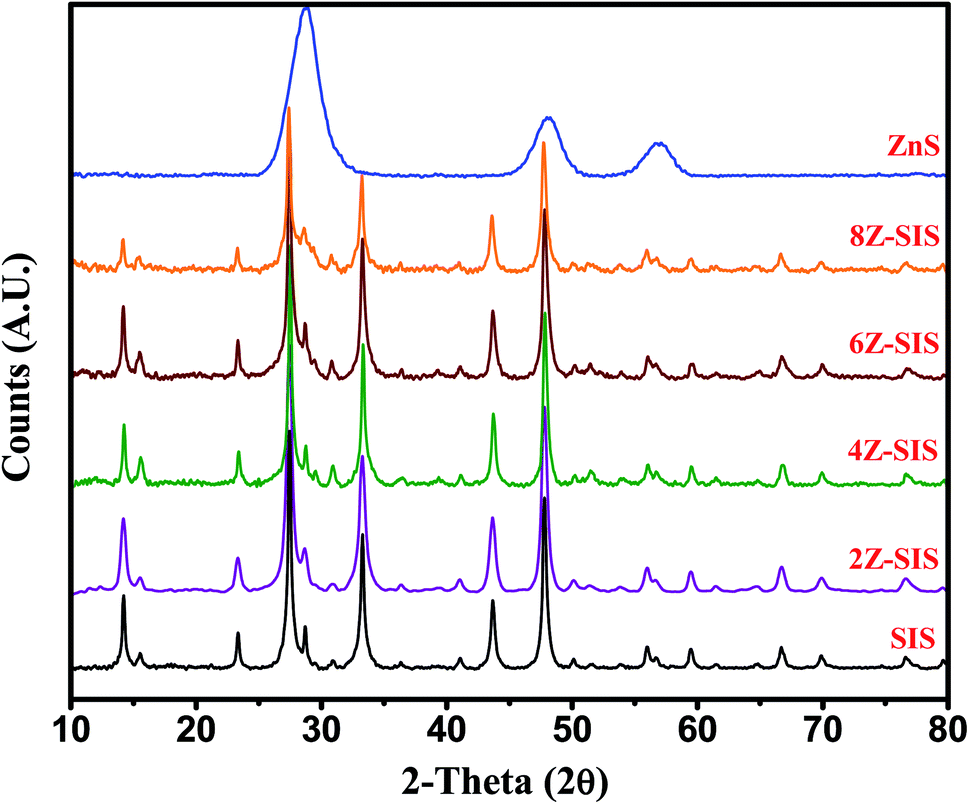 | ||
| Fig. 1 XRD pattern for SnIn4S8 NPs, ZnS NPs and ZnS/SnIn4S8 nanoheterostructure with different Z/S molar ratios. | ||
2.5 Photocatalytic test
The photocatalytic activities of the as prepared photocatalysts were evaluated by photocatalytic reduction of Cr(VI) in an aqueous solution under natural solar irradiation. In a typical experiment, about 50 mg of the photocatalyst was added to a 100 mL of Cr(VI) solution with a concentration of 50 mg L−1. The pH of mixed solution was adjusted at 3.0 with diluted H2SO4 solution. Prior to irradiation, the solution was magnetically stirred in the dark for 60 min to reach the adsorption–desorption equilibrium. The intensity of the natural sun was measured from March 15 to April 10, 2021 in our laboratory at Kuwait University, Khaldiya campus (29.9450° N, 31.0640° E) in days with a shiny sky without clouds. The incident solar radiation was measured by digital illumination meter (INS, DX-200) around 82.300 flux (656 W m−2). After each 20 minutes, 3.0 mL aliquots of Cr(VI) solutions were taken and spectrophotometrically measured. Each time, the suspension was centrifuged to exclude the nanoparticles from the solution. The Cr(VI) photodegradation kinetics was studied by recording the absorption spectra (at λmax = 348 nm). The photodegradation was calculated according as follow:
 | (1) |
2.6 Electrochemical performance
A three-electrode system was used to test Mott–Schottky plots in a 1.0 M Na2SO4 aqueous solution at 25 °C. By spreading the heterostructures (10 mg) in a methyl alcohol solution (1 mL), the glass carbon (GC) working electrode was modified in this slurry. The slurry was sonicated for 10 minutes and dried on the GC electrode surface at room temperature for 3 hours. A modified electrode surface was further treated by adding 5.0 mL (0.25%) of Nafion solution as a binder and dried at 70 °C for 1 hour. As the counter and reference elements, the platinum wire and Ag/AgCl respectively were used. The measurements of Mott–Schottky were performed with the potential from −1.5 V to 1.5 V with a step potential of 0.05 V and 10 kHz frequency.3. Results and discussions
3.1 Structural characterization of ZnS/SnIn4S8 nanoheterostructures
The XRD patterns of the prepared nanoparticles were investigated as shown in Fig. 1. For SnIn4S8, the peaks at 14.32°, 23.42°, 27.49°, 33.36°, 43.69° and 47.88° were assigned to (111), (220), (311), (400), (333) and (440) crystal face (JCPDS card no. 42-1305), this corresponded to prior findings.16 For ZnS pattern, the peaks located at 2θ values of 28.84, 48.71 and 58.14 were assigned to (111), (220) and (311) are corresponded to ZnS zinc blende (JCPDS no. 80-0020).17,18 In the patterns of ZnS/SnIn4S8 nanoheterostructures, both ZnS and SnIn4S8 major diffraction peaks were found, indicating that ZnS and SnIn4S8 combination was successful. The crystallite sizes of bare SnIn4S8 and ZnS nanoparticles were ∼4.62 and ∼2.7 nm respectively as calculated from the Scherrer equation. D = 0.89λ/(βcosθ).19
X-ray photoelectron spectroscopy (XPS) was utilized to further explore the element composition and chemical states in 20% ZnS/SnIn4S8 (2Z-SIS) as a model sample which exhibit the highest photocatalytic activity, and the complete scan XPS spectra clearly confirmed the existence of S, In, Sn, and O in the 2Z-SIS nanoheterostructure. In Fig. 2A–D, the high resolution XPS spectra of Sn3d with two peaks at 486.2 (Sn3d5/2) and 494.6 eV (Sn3d3/2) and In3d with two peaks at 445.1 (In3d5/2) and 452.5 eV (In3d3/2) that are well-agreed with formation of the Sn4+ state and In3+ state, respectively, this was consistent with prior findings.20 Meanwhile, the S2p area of the high resolution XPS spectra for SnIn4S8 (Fig. 2C) could be separated into two peaks at roughly 161.6 and 162.7 eV, corresponding to the S2p3/2 and S2p1/2 respectively.20 The binding energy values of Zn2p3/2 and Zn2p1/2 (Fig. 2D) were found at 1021.63 eV and 1044.79 eV, assigned to the Zn2+.21 Finally, the high resolution XPS spectra of the S2p region for ZnS (Fig. 2E) are deconvoluted into two peaks located at 161.62 and 162.6 eV, which are corresponding to the S2p3/2 and S2p1/2 states respectively.22 In addition, as shown in Fig. 2F, the valence bands (VB) of both ZnS and SnIn4S8 are determined using valence band XPS to confirm the energy band locations.23 ZnS exhibits a VB with a maximum energy edge of around 2.77 eV. For SnIn4S8, however, the VB maximum energy up shifts to 1.63 eV, compared with that of ZnS.
 | ||
| Fig. 2 XPS spectra for 2Z-SIS nanoheterostructure: (A) Sn 3d, (B) In 3d, (C) S 2p for SIS, (D) Zn 2p, (E) S 2p for ZnS and (F) valence band for ZnS and SnIn4S8 nanoparticles. | ||
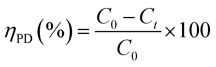
The morphology of the as-synthesized samples was examined by TEM as shown in Fig. 3. The microscopy images revealed that SIS exhibit wrinkle, ultrathin, and layered structures. For ZnS, the nanoparticles revealed a semi-spherical shape without agglomeration with an average particle size of 8.0 nm. For 2Z-SIS nanoheterostructure, the image revealed the inclusion of ZnS NPs on the surface of SIS without noticeable aggregation.
 | ||
| Fig. 3 TEM images for SnIn4S8 NPs, ZnS NPs and ZnS/SnIn4S8 nanoheterostructure. The scale bar is 50 nm. | ||
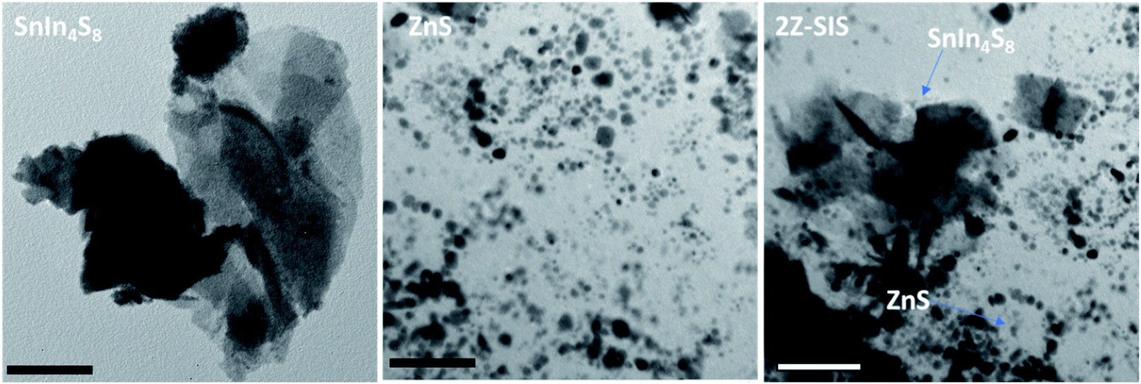
The surface area and porous structure of bare ZnS and SnIn4S8 nanoparticles and their nanoheterostructures with different molar ratios were investigated using N2 adsorption–desorption isotherms as shown in Fig. 4. From the figure, the isotherms of both ZnS and SnIn4S8 nanoparticles show a type IV shape with an H3 hysteresis loop in the region of 0.4–0.9 p/p0. The specific surface area (SBET) and other textural properties are tabulated in Table 1. The results revealed that the incorporation of ZnS in SnIn4S8 caused increasing in its surface area at the first molar ratio 20% (2Z-SIS) and the further increase in the molar ratio resulted in slight decrease in the surface area. This phenomenon most likely attributed to the small average particle size of ZnS rather than the SnIn4S8 pore diameter.
 | ||
| Fig. 4 N2 adsorption–desorption isotherm for ZnS, SnIn4S8 and ZnS/SnIn4S8 nanoheterostructures. | ||
| Sample | SBET | Pore volume | Pore size | Crystallite size | Band gap | Rate, min−1 |
|---|---|---|---|---|---|---|
| ZS | 88.92 m2 g−1 | 0.08 cm3 g−1 | 3.7 nm | 2.5 | 3.43 | 2.1 × 10⁻³ |
| SIS | 78.63 m2 g−1 | 0.13 cm3 g−1 | 6.4 nm | 4.62 | 2.60 | 5.1 × 10⁻³ |
| 2Z-SIS | 91.16 m2 g−1 | 0.14 cm3 g−1 | 6.3 nm | 3.66 | 2.63 | 7.8 × 10⁻³ |
| 4Z-SIS | 66.73 m2 g−1 | 0.09 cm3 g−1 | 6.5 nm | 3.54 | 2.57 | 6.2 × 10⁻³ |
| 6Z-SIS | 72.95 m2 g−1 | 0.11 cm3 g−1 | 5.8 nm | 3.61 | 2.54 | 5.8 × 10⁻³ |
| 8Z-SIS | 70.31 m2 g−1 | 0.11 cm3 g−1 | 4.6 nm | 3.50 | 2.61 | 5.5 × 10⁻³ |
The isoelectric point (pHiep) is the pH value at which the NPs' surface charge equals zero. The nanoparticles have a surface charge above and below the pHiep, which causes repulsion and keeps the solution colloidally stable.24 Therefore, the zeta potential (ζ) measurements in Fig. 5 gave insights about the nanoparticles surface charge. It revealed that the pHiep of a ZnS NPs is at 4.5 and that of SnIn4S8 at 8.1 which are matched with previously reported values.18 This finding shows mapping of the surface of ZnS/SnIn4S8 nanoheterostructures that it bears a positive charge below pH 7.2 in case of 2Z-SIS and bears a positive charge above this pH value.
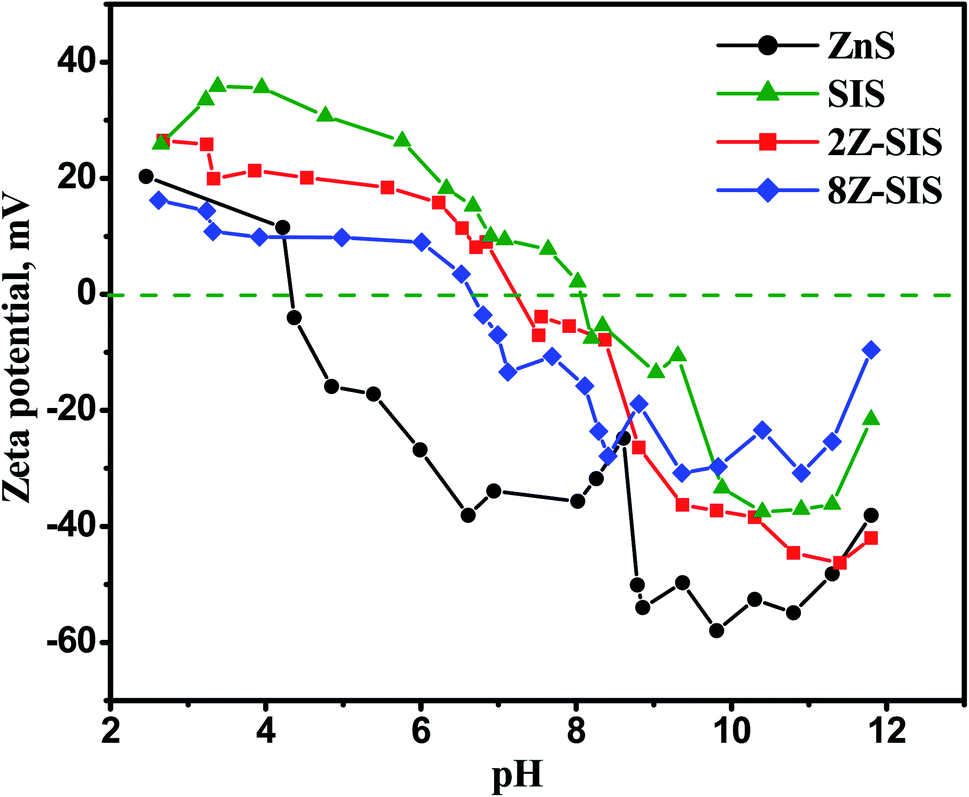 | ||
| Fig. 5 Zeta potential measurements of ZnS, SnIn4S8 and ZnS/SnIn4S8 nanoheterostructures. | ||
The optical characteristics of the prepared nanoheterostructures were investigated through the UV Vis spectrum (Fig. 6). ZnS NPs is a UV active substance that has a maximum absorption in the ultraviolet region at 361 nm. The absorption spectrum shown for SnIn4S8 confirmed its optical response in the visible region.25 A substantial increase in absorption (hyperchromic effect) was noted for ZnS/SnIn4S8 nanoheterostructures and at about 500 nm. By applying Tauc equation, the optical band gaps (Eg) of nanoheterostructures were estimated: (αhν)1/m = k(hν − Eg); where Eg is the optical bandgap energy, k is a constant and m = 1/2 for a direct energy bandgap and m = 2 for indirect energy bandgap.26,27 ZnS, SnIn4S8 and ZnS/SnIn4S8 nanoheterostructures were characterized by direct transitions as indicated from Tauc plots (not shown) with bandgaps of 3.43, 2.60 and 2.75 eV, respectively.
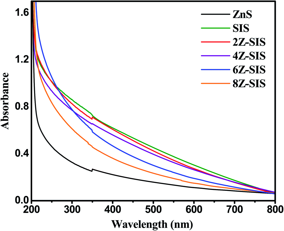 | ||
| Fig. 6 UV-vis absorption spectra of ZnS, SnIn4S8 and ZnS/SnIn4S8 nanoheterostructures. | ||
3.2 Photocatalytic reduction of Cr(VI)
The photocatalytic activity of the prepared nanoheterostructures was examined toward the photocatalytic reduction of Cr(VI) contaminant under sunlight irradiation. The photocatalytic reduction of Cr(VI) was followed up by recording the absorbance change at 348 nm as a function of irradiation time. The photocatalytic reduction rate of Cr(VI) obtained using 2Z-SIS was markedly higher than that attained by using SIS. For SIS, the Cr(VI) photoreduction rate obtained was only 61.0%, while for 2Z-SIS, the Cr(VI) photoreduction was enhanced up to 92.3%. The photoreduction rate constant (k) was determined using the following eqn: lnC0/Ct = kt as shown in Fig. 7A and Table 1. Where, Ct is the concentration at specific time, C0 is the initial concentration, k is a photodegradation rate constant (min−1), and t is reaction time in (min). A plot of lnA0/A against photodegradation time (Fig. 7A) exhibited a linear trend and from the slope of the line the apparent first-order rate constant k was obtained and tabulated in Table 1. From Fig. 7A, the reaction follows a pseudo-first-order rate.
 | ||
| Fig. 7 (A) Kinetics for Cr(VI) photocatalytic degradation using ZnS, SnIn4S8 and ZnS/SnIn4S8 nanoheterostructures (B) reusability results of 2Z-SIS nanoheterostructure. | ||
To test the stability and regeneration capability of the investigated photocatalysts, four repeated photodegradation cycles were performed with the 2Z-SIS nanoheterostructure to test the reusability of the photocatalyst. At each cycle, the photocatalyst was washed then treated at 50 °C until it was completely dry and then used for the next cycle. The results presented in Fig. 7B proved the photostability and reactivity of the 2Z-SIS nanoheterostructure. After the 4th cycle, the photo catalytic activity of the 2Z-SIS nanophotocatalyst was not notably decreased.
3.3 Photocatalytic mechanism
In order to anticipate the mechanism pathway of photodegradation, energy levels of both the valence band (EVB) and conduction band (ECB) are crucial in relation to the standard redox potential (Eo). Therefore, it is vital to explore its band structure in order to support the mechanism of action for photocatalytic systems. Therefore, in this section, Mott-plots Schottky's have been studied to elucidate the ZnS/SnIn4S8 nanoheterostructure band structure.Mott–Schottky plots for ZnS and SnIn4S8 NPs revealed a positive slope trend which is an indication for their n-type nature.28 And their ZnS/SnIn4S8 nanoheterostructure revealed a n–n heterojunction as shown in Fig. 8. The flat band, Efb, values were estimated by extending the linear fit line from 1/C2 versus E plot. The Efb of ZnS, SnIn4S8 and ZnS/SnIn4S8 NPs were determined to be −0.77, −1.33 and −1.21 V vs. SCE respectively which are corresponding to −0.53, −1.10 and −0.97 V vs. NHE respectively as E(NHE) = E(SCE) + 0.242 V.29 The potential for n-type semiconductors is substantially higher by 0.1–0.3 eV, depending on the effective electron mass and carrier concentration than the flat band potential.30 The difference in potentials between conduction and flat bands has been set at 0.2 eV in this experiment. Therefore, the bottom of the conduction band for ZnS and SnIn4S8 NPs, ECB, were found to be −0.73 and −1.40 eV, respectively. The VB potential values (EVB) were found to be 2.7 and 1.2 eV for ZnS and SnIn4S8 NPs respectively based on their optical band gap values.
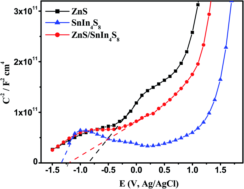 | ||
| Fig. 8 Mott–Schottky plots of ZnS, SnIn4S8 and ZnS/SnIn4S8 nanoheterostructures in 0.1 M Na2SO4 at a frequency of 10000 Hz. | ||
By exploring the CB and VB positions for ZnS and SnIn4S8 NPs, the charge carrier transfer process of photogenerated electron and holes in the ZnS/SnIn4S8 nanoheterostructure could be proposed via two possible ways: traditional (type-II) (Scheme 1) or direct S-scheme as shown in Scheme 1. The formation of reactive species that are responsible for photoactivity in nanoheterostructures are shown in Scheme 1 based on data collected from Mott–Schottky plots. In the first proposed mechanism traditional type-II pathway, upon photoexcitation, the electrons generated on the CB of SnIn4S8 can reduce O2 into ˙O2− radicals because the CB position is more negative than that of the ˙O2−/O2 (−0.33 eV vs. NHE), and ZnS has a more positive VB potential (2.7 eV vs. NHE) than ˙OH/H2O (H2O/˙OH, 2.40 eV vs. NHE), meaning that the photoexcited holes of ZnS can oxidize the absorbed H2O molecules to generate ˙OH. The electrons on the SnIn4S8 CB can move to the ZnS CB and leave holes on the SnIn4S8 VB because the CB potential of the SnIn4S8 is more negative than that of ZnS. Meanwhile, because ZnS exhibit a more positive VB potential than SnIn4S8, the hole of ZnS travels to the VB of SnIn4S8. If this assumption is, nevertheless, appropriate, the h+ accumulated in the VB of SnIn4S8 (1.2 eV) could not reduce H2O to ˙OH (H2O/˙OH, 2.40 eV vs. NHE). Therefore, it can be fairy proposed that the photo-generated charge carrier transfer within ZnS/SnIn4S8 nanoheterostructure follows the S-scheme pathway. In this proposed mechanism pathway, the combination was achieved between the electrons in the CB of ZnS and the holes in the VB of SnIn4S8, so the electrons in the CB of SnIn4S8 and the holes in the VB of ZnS can be retained. Then the ZnS/SnIn4S8 nanoheterostructure can generate ˙O2− and ˙OH, because SnIn4S8 has a more negative CB potential and ZnS has a more positive VB potential.
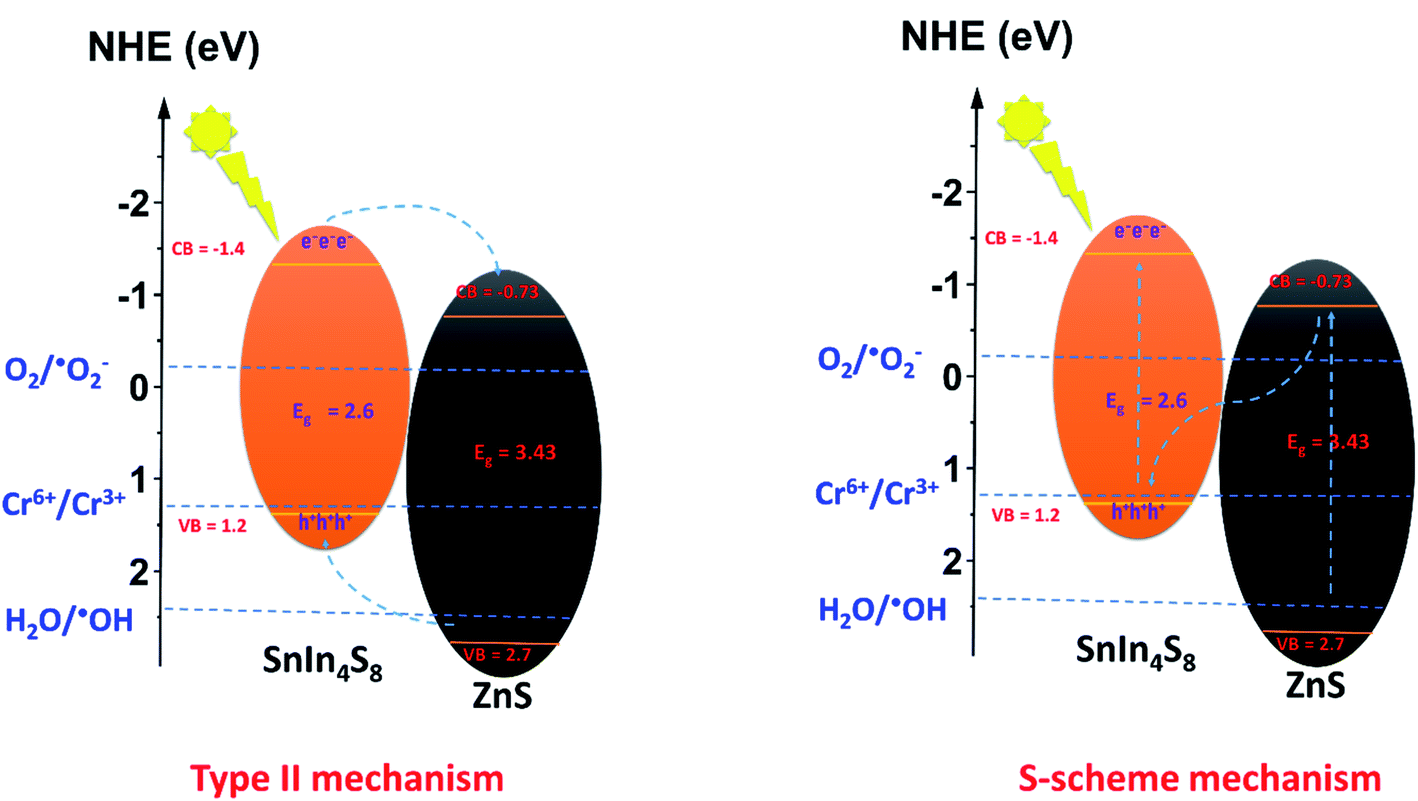 | ||
| Scheme 1 Schematic diagram of the proposed mechanism pathways of ZnS/SnIn4S8 nanoheterostructure. | ||
4. Conclusion
S-scheme photocatalysts based on ZnS/SnIn4S8 nanoheterostructures were successfully prepared and characterized to be used as a solar active photocatalyst for Cr(VI) photoreduction. The optoelectronic features of the heterostructure were shown to have an excellent potential for photodegrading Cr(VI) under sunlight. The photoreduction tests demonstrated an improved photocatalytic activity of SIS and 2Z-SIS to be 61.0% and 92.3% respectively which after 120 min under the same conditions. The acquired findings indicated the photocatalyst's capability under natural sun radiation, allowing for its industrial use.Conflicts of interest
There are no conflicts to declare.Acknowledgements
The researchers appreciate the support of the Research Administration at Kuwait University via RSPU, Facilities No. (GS 01/01, GS 01/05, GS 02/01, GE 03/08, GE 01/07 and GS 03/01). Also, Nanoscopy science center is highly acknowledged.References
- M. C. Chattopadhyaya, M. G. Soares, M. T. de Jesus Simões Campos Tavares, S. Ismadji, G. Lofrano, M. A. Barakat, K. Ikehata, X. B. Yin, P. Chowdhury and S. K. Sharma, Heavy Metals In Water: Presence, Removal and Safety, Royal Society of Chemistry, 2014 Search PubMed.
- X. Wang, S. O. Pehkonen and A. K. Ray, Ind. Eng. Chem. Res., 2004, 43, 1665–1672 CrossRef CAS.
- J. Li and N. Wu, Catal. Sci. Technol., 2015, 5, 1360–1384 RSC.
- M. Zhou, K. Xiao, X. Jiang, H. Huang, Z. Lin, J. Yao and Y. Wu, Inorg. Chem., 2016, 55, 12783–12790 CrossRef CAS PubMed.
- L. Nie and Q. Zhang, Inorg. Chem. Front., 2017, 4, 1953–1962 RSC.
- N. Chumha, W. Pudkon, A. Chachvalvutikul, T. Luangwanta, C. Randorn, B. Inceesungvorn, A. Ngamjarurojana and S. Kaowphong, Mater. Res. Express, 2020, 7, 015074 CrossRef CAS.
- S. Li, X. Tang, Z. Zang, Y. Yao, Z. Yao, H. Zhong and B. Chen, Chin. J. Catal., 2018, 39, 590–605 CrossRef CAS.
- M. Madkour, H. A. E. Nazer and Y. K. Abdel-Monem, 11 – Use of chalcogenides-based nanomaterials for photocatalytic heavy metal reduction and ions removal, in Chalcogenide-Based Nanomaterials as Photocatalysts, ed. M. M. Khan, Elsevier, 2021, pp. 261–283 Search PubMed.
- Q. Li, X. Li and J. Yu, Chapter 10 – Surface and interface modification strategies of CdS-based photocatalysts, in Interface Science and Technology, ed. J. Yu, M. Jaroniec and C. Jiang, Elsevier, 2020, pp. 313–348 Search PubMed.
- Y. Song, J. Zhang, X. Dong and H. Li, Energy Technol., 2021, 9, 2100033 CrossRef CAS.
- M. I. A. Abdel Maksoud, A. G. Bedir, M. Bekhit, M. M. Abouelela, R. A. Fahim, A. S. Awed, S. Y. Attia, S. M. Kassem, M. A. Elkodous, G. S. El-Sayyad, S. G. Mohamed, A. I. Osman, A. a. H. Al-Muhtaseb and D. W. Rooney, Environ. Chem. Lett., 2021 DOI:10.1007/s10311-021-01268-x.
- F. Al-Sagheer, A. Bumajdad, M. Madkour and B. Ghazal, Sci. Adv. Mater., 2015, 7, 2352–2360 CrossRef CAS.
- K. Yu, H.-B. Huang, J.-T. Wang, G.-F. Liu, Z. Zhong, Y.-F. Li, H.-L. Cao, J. Lü and R. Cao, J. Mater. Chem. A, 2021, 9, 7759–7766 RSC.
- F. Deng, X. Lu, L. Zhao, Y. Luo, X. Pei, X. Luo and S. Luo, J. Mater. Sci., 2016, 51, 6998–7007 CrossRef CAS.
- P. Xu, S. Huang, M. Liu, Y. Lv, Z. Wang, J. Long, W. Zhang and H. Fan, Catalysts, 2019, 9, 187 CrossRef.
- H. Li, W. Song, X. Cui, Y. Li, B. Hou, L. Cheng and P. Zhang, Nanoscale Res. Lett., 2021, 16, 10 CrossRef CAS PubMed.
- A. Wang, H. Shen, S. Zang, Q. Lin, H. Wang, L. Qian, J. Niu and L. Song Li, Nanoscale, 2015, 7, 2951–2959 RSC.
- M. Madkour and F. Al Sagheer, Opt. Mater. Express, 2017, 7, 158–169 CrossRef CAS.
- N. Shanmugam, K. Dhanaraj, G. Viruthagiri, K. Balamurugan and K. Deivam, Arabian J. Chem., 2016, 9, S758–S764 CrossRef CAS.
- Y. Lv, Z. Yu, S. Huang, F. Deng, K. Zheng, G. Yang, Y. Liu, C. Lin, X. Ye and M. Liu, Chemosphere, 2021, 271, 129452 CrossRef CAS PubMed.
- S. K. Maji, N. Mukherjee, A. Mondal, B. Adhikary, B. Karmakar and S. Dutta, Inorg. Chim. Acta, 2011, 371, 20–26 CrossRef CAS.
- M. BinSabt, A. A. Nazeer, M. Madkour and F. Al-Sagheer, RSC Adv., 2016, 6, 6888–6895 RSC.
- A. G. Joshi, S. Sahai, N. Gandhi, Y. G. R. Krishna and D. Haranath, Appl. Phys. Lett., 2010, 96, 123102 CrossRef.
- E. Al-Hetlani, M. O. Amin and M. Madkour, Appl. Surf. Sci., 2017, 411, 355–362 CrossRef CAS.
- S. Zhang, B. Zhang, Y. Jiang, Y. Xiao, W. Zhang, H. Xu, X. Yang, Z. Liu and J. Zhang, Appl. Surf. Sci., 2021, 542, 148618 CrossRef CAS.
- E. Al-Hetlani, O. Amin Mohamed and M. Madkour, Nanophotonics, 2018, 683 CAS.
- R. Zamiri, H. A. Ahangar, A. Zakaria, G. Zamiri, M. Shabani, B. Singh and J. Ferreira, Chem. Cent. J., 2015, 9, 28 CrossRef PubMed.
- D. Boosagulla, S. Mandati, R. Allikayala and B. V. Sarada, ECS J. Solid State Sci. Technol., 2018, 7, P440–P446 CrossRef CAS.
- T. Pacześniak, P. Błoniarz, K. Rydel and A. Sobkowiak, Electroanalysis, 2007, 19, 945–951 CrossRef.
- H. Kisch, Angew. Chem., Int. Ed., 2013, 52, 812–847 CrossRef CAS PubMed.
| This journal is © The Royal Society of Chemistry 2021 |