
 Open Access Article
 This Open Access Article is licensed under a Creative Commons Attribution-Non Commercial 3.0 Unported Licence
Predictions of moiré excitons in twisted two-dimensional organic–inorganic halide perovskites†
Linghai
Zhang
 ,
Xu
Zhang
and
Gang
Lu
*
,
Xu
Zhang
and
Gang
Lu
*
Department of Physics and Astronomy, California State University, Northridge, California 91330-8268, USA. E-mail: ganglu@csun.edu
First published on 23rd March 2021
Abstract
Recent breakthrough in synthesizing arbitrary vertical heterostructures of Ruddlesden–Popper (RP) perovskites opens doors to myriad quantum optoelectronic applications. However, it is not clear whether moiré excitons and flat bands can be formed in such heterostructures. Here, we predict from first principles that twisted homobilayers of RP perovskite, MA2PbI4, can host moiré excitons and yield flat energy bands. The moiré excitons exhibit unique and hybridized characteristics with electrons confined in a single layer of a striped distribution while holes localized in both layers. Nearly flat valence bands can be formed in the bilayers with relatively large twist angles, thanks to the presence of hydrogen bonds that strengthen the interlayer coupling. External pressures can further increase the interlayer coupling, yielding more localized moiré excitons and flatter valence bands. Finally, electrostatic gating is predicted to tune the degree of hybridization, energy, position and localization of moiré excitons in twisted MA2PbI4 bilayers.
Introduction
Moiré superlattices have emerged as a fascinating platform to pursue fundamental science and novel applications in two-dimensional (2D) van der Waals (vdW) materials.1–6 The energy bands in the moiré superlattices can be folded into mini-Brillouin zones and nearly “flat” energy bands may be formed,7–9 which enhances the role of electron–electron correlations and gives rise to exotic physical phenomena, such as unconventional superconductivity,1,10 novel Mott and Wigner crystals,2,11 fractal quantum Hall effect,12etc. In particular, moiré excitons have been observed in vdW heterostructures of stacked 2D layers of transition metal dichalcogenides (TMDs).13–18 These long-lived, localized and valley-polarized moiré excitons are envisioned as single-photon emitters in quantum information and optoelectronic devices19,20 and as a means to realizing Bose–Einstein condensation.21Moiré superlattices can emerge in vdW heterostructures with a small angular or lattice mismatch, and controlling the twist angle (θ) of 2D layers could lead to enhancement of electron interactions and localization of excitonic states.17,22–24 For example, recent theoretical and experiment studies have reported the formation of flat energy bands25,26 and localized moiré excitons14,15,17 in TMD bilayers with small twist angles. An important but unanswered question is whether moiré excitons and flat bands can also be formed in heterostructures of 2D semiconductors other than TMDs. If yes, can they be formed with a larger twist angle and a broader tunability? Do these moiré excitons exhibit distinct characteristics? Answering these questions would certainly expand and advance the research frontiers in this burgeoning field and more importantly could open doors to unprecedented applications.
Here, we predict that vdW heterostructures of 2D Ruddlesden–Popper (RP) halide perovskites could host moiré excitons with flat energy bands. The RP halide perovskites have a general chemical formula of (LA)2An−1PbnX3n+1, where LA is a long-chain alkylammonium cation, A is a small cation, such as methylammonium (MA), X is a halide anion and n is an integer. Like TMDs, the RP perovskites possess large exciton binding energies in the range of 0.1–0.5 eV,27–32 depending on n value and the dielectric environment (e.g., LA cations). Compared to TMDs, the RP perovskites exhibit a unique and broader tunability in their molecular structures and chemical compositions. As a result, the RP perovskites have shown tremendous potentials in diverse optoelectronic applications, such as photovoltaics,33 light-emitting diodes,34 lasers,35 photodetectors,36etc. Recently, a breakthrough was made in deterministic fabrication of arbitrary vertical heterostructures of 2D RP perovskites,37 which promises an access to an expanding library of 2D perovskite building blocks and enables unprecedented control of their heterostructures. Furthermore, impressive progress has been made to fold vdW materials at a defined position and direction using microfluidic forces;38 this technique could potentially be used to form 2D perovskite bilayers with precise twist angles. However, despite the synthetical triumphs, it is not clear whether moiré excitons and flat bands can be formed in 2D RP perovskite heterostructures to enable the envisioned quantum and optoelectronic applications.
In this work, we aim to fill this knowledge gap and explore optoelectronic properties of 2D perovskite heterostructures from first principles. More specifically, both non-twisted (θ = 0°) and twisted (θ = 8.1° and θ = 11.3°) homobilayers of 2D RP perovskite (MA2PbI4) are examined. MA2PbI4 is one of the simplest 2D RP perovskites with superior stability thanks to hydrogen (H) bonds at its surface.39,40 Based on first-principles calculations, we predict that localized moiré excitons can be formed in twisted MA2PbI4 homobilayers. Computational methods and details are included in the ESI.† These moiré excitons exhibit unique characteristics with localized holes in both layers and a quasi-one-dimensional (1D) distribution of electrons in a single layer. Nearly flat valence bands can be formed at larger twist angles as compared to TMD bilayers, with the top valence bandwidth approaching zero for the bilayer of θ = 8.1°. The relative ease in the flat band formation is attributed to the interlayer H bonds, which enhance the interlayer coupling and deepen the moiré potential. External pressures can further increase the interlayer coupling and yield more localized moiré excitons and flatter valence bands. Lastly, we predict that electrostatic gating can tune the degree of hybridization, energy, position and localization of the moiré excitons in the twisted bilayers.
Results and discussion
We first examine non-twisted MA2PbI4 homobilayers (θ = 0°), setting the stage for ensuing discussions. Although there is no relative twist between the monolayers, diverse stacking configurations can nonetheless appear in the homobilayers.41,42 Here, we consider four representative stacking configurations (termed as A, B, C, and D), whose atomic structures are displayed in Fig. 1; these configurations could also exist as local motifs in twisted MA2PbI4 bilayers. We have calculated the binding energies of the four homobilayers and found them to be energetically stable (Table S1 in the ESI†). Among the four configurations, A is energetically most stable while B is least stable. A unique feature of the 2D RP perovskite MA2PbI4 is the presence of interlayer H bonds. These H bonds can be characterized by their bond lengths, i.e., the shortest distances between H in NH3 group of the interfacial MA cation and I ions in the top or bottom layer, shown schematically in Fig. 2a. As summarized in Table S1,† the most stable configuration A has the shortest H bond lengths whereas the least stable configuration B has the longest H bond lengths. The combination of vdW interaction and H bonds is expected to strengthen the interlayer coupling in the RP perovskite heterostructures, compared to TMD bilayers which do not have such H bonds.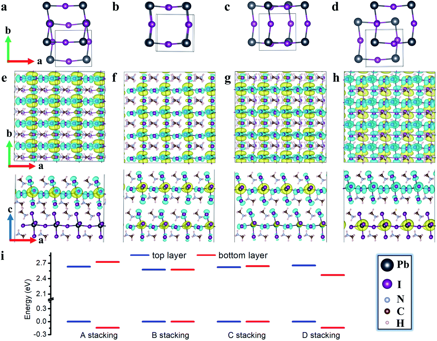 | ||
| Fig. 1 (a–d) The unit cells of the four stacking configurations (not all atoms are displayed for visual clarity). (e–h) The charge density of the lowest energy exciton for the stacking configuration A, B, C, D, respectively, in a 4 × 4 × 1 supercell. The hole and electron densities (iso-surface value set at 0.0001 e Å−3) are shown in cyan and yellow color, respectively. (i) The band alignment of A, B, C, and D stacking configurations with VBM set to zero. | ||
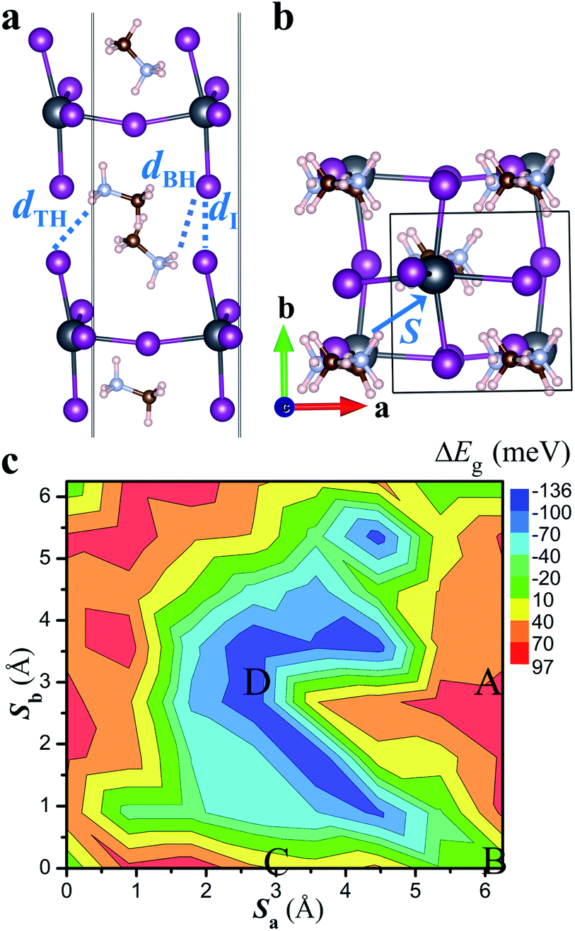 | ||
| Fig. 2 (a) Schematic diagram showing interfacial ions and their shortest distances (dI, dTH and dBH). dTH (dBH) represents the distance between I and H (in NH3 group) at the top (bottom) layer. (b) Definition of the interlayer displacement vector (S) in the primitive unit cell of the non-twisted MA2PbI4 bilayer. (c) The band gap variation (ΔEg) as a function of the interlayer displacement vector S (Sa and Sb are the projections of S in a and b axis). The approximate locations of the four stacking configurations are also indicated. | ||
The charge density of the lowest energy exciton in the non-twisted MA2PbI4 bilayers is displayed in Fig. 1e–h. The exciton is delocalized in the 2D layer, irrespective of the stacking configurations; similar observations are also found for higher energy excitons. Thus, there is no apparent moiré potential in the non-twisted MA2PbI4 bilayers. The exciton in the A stacking exhibits a strong intralayer characteristic, with both its electron and hole (and the dipole moment) confined in the top layer. The exciton in the D stacking, on the other hand, shows an interlayer characteristic, with its electron and hole separated in the different layers and presence of a large vertical dipole moment (Table S1†). The stacking B and C yet yield hybridized excitons with both intralayer and interlayer characteristics. The existence of diverse exciton species in the same homobilayers has also been observed in TMDs.43,44 As shown in Fig. 1i, the formation of the intralayer exciton in the stacking A arises from its type-I band alignment, whereas the formation of the interlayer exciton in the stacking D results from its type-II band alignment. The small band offsets in the stacking B and C, on the other hand, yield the hybridized excitons. Hence, the excitonic properties of perovskite heterostructures can be tuned by the interlayer translations and rotations, and particularly in twisted bilayers where a variety of local stacking configurations can co-exist. The exciton binding energy is estimated as 0.20, 0.20, 0.20 and 0.16 eV for the A, B, C, and D stacking configuration, respectively, which is close to the value (0.17 eV) reported in bulk MA2PbI4.39
Moiré potentials play a crucial role in the formation of flat energy bands and localization of moiré excitons in vdW heterostructures. We subsequently estimate the moiré potential in MA2PbI4 bilayers by the spatial variation of the bandgap as a function of relative displacements of the two layers.15,45 As displayed in Fig. 2b, the relative displacement between the two layers is represented by a vector S defined in the primitive unit cell of the non-twisted MA2PbI4 bilayer. As S spans across the entire unit cell, all possible stacking configurations may be obtained. Fig. 2c shows the bandgap variation, ΔEg(S) = Eg(S) − 〈Eg〉, as a function of the displacement S. Eg is the energy difference between the conduction band minimum (CBM) and the valence band maximum (VBM) of the non-twisted MA2PbI4 bilayer and 〈Eg〉 is the average value of Eg. The moiré potential well (−136 meV) is found at the center of the unit cell, corresponding to the stacking D, while the moiré potential crest (97 meV) is close to the stacking A. The amplitude of the moiré potential (233 meV) in MA2PbI4 bilayers is slightly smaller than that in MoS2/WS2 bilayers.15 However, the extrema of the moiré potential in MA2PbI4 bilayers are not as clearly defined as those in MoS2/WS2 bilayers, probably due to “lattice softness” of the RP perovskites. In particular, the organic cations (MA) in MA2PbI4 present as additional degrees of freedom and their rotations could modulate the moiré potential significantly.
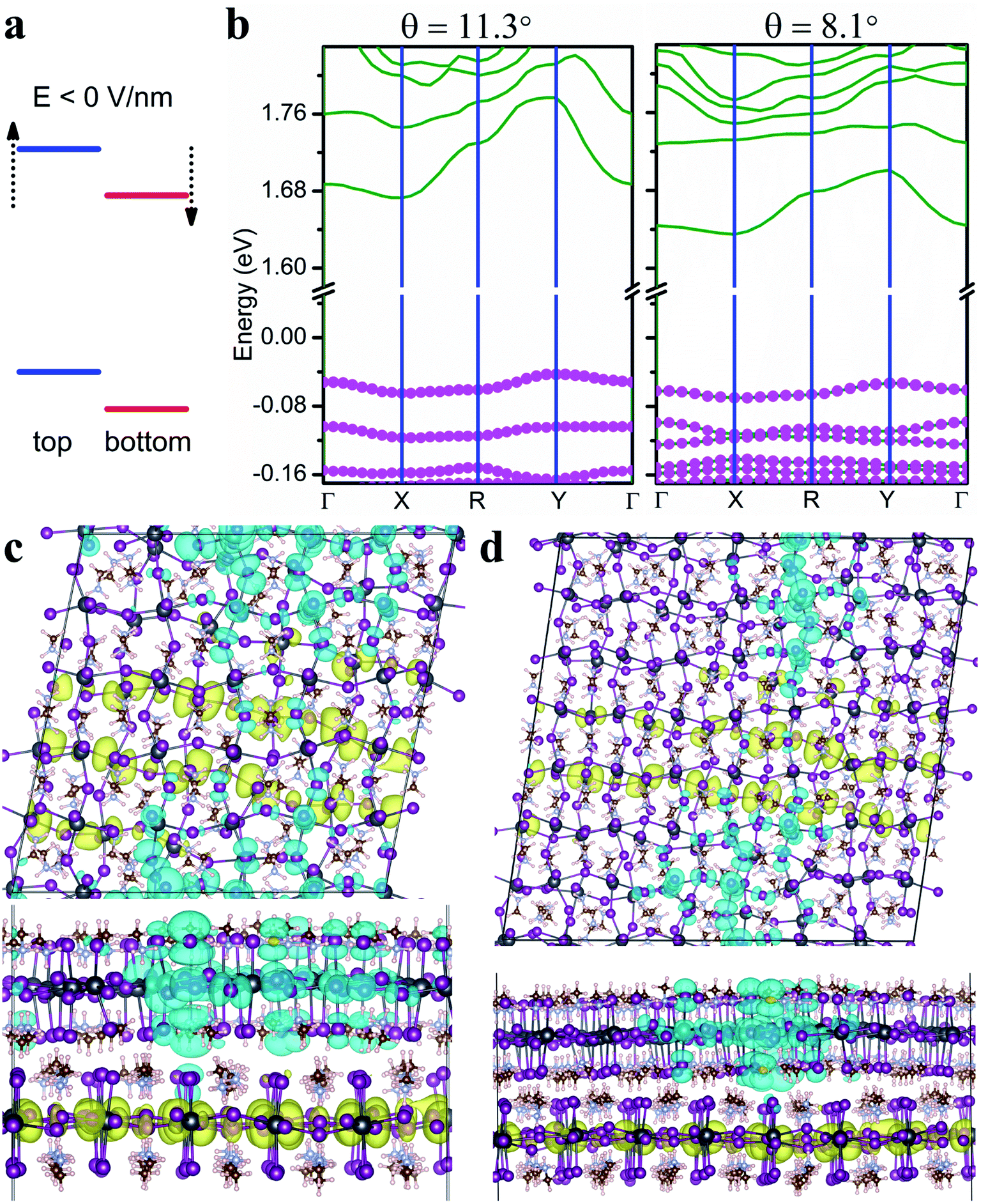
In the following, we focus on two twisted MA2PbI4 homobilayers with twist angle θ = 11.3° and θ = 8.1°, whose molecular structures are shown in Fig. S1.† The supercell of the periodic moiré superlattice contains 1050 and 2058 atoms for θ = 11.3° and 8.1°, respectively (Fig. 3a and b). The single-particle band structures for both twisted bilayers are displayed in Fig. 3c and d. For both twisted bilayers, the valence bands are narrower than the conduction bands, and the bandwidths in θ = 8.1° are smaller than the corresponding ones in θ = 11.3°; these general trends are the same as in twisted TMD bilayers.15 Nearly flat valence bands are formed in both moiré superlattices, with a vanishing VBM bandwidth (∼0 meV) in θ = 8.1° twisted bilayer. The VBM bandwidth in θ = 11.3° bilayer is slightly larger (9–11 meV in Table S2†). Compared to MoS2/WS2 bilayers (θ < 3.48°),15 the formation of flat VBM bands in MA2PbI4 bilayers occurs at a much larger twist angle (θ = 8.1°). As a reference, the VBM bandwidth in non-twisted MA2PbI4 bilayer (A stacking) is 321 meV (Fig. 3g).
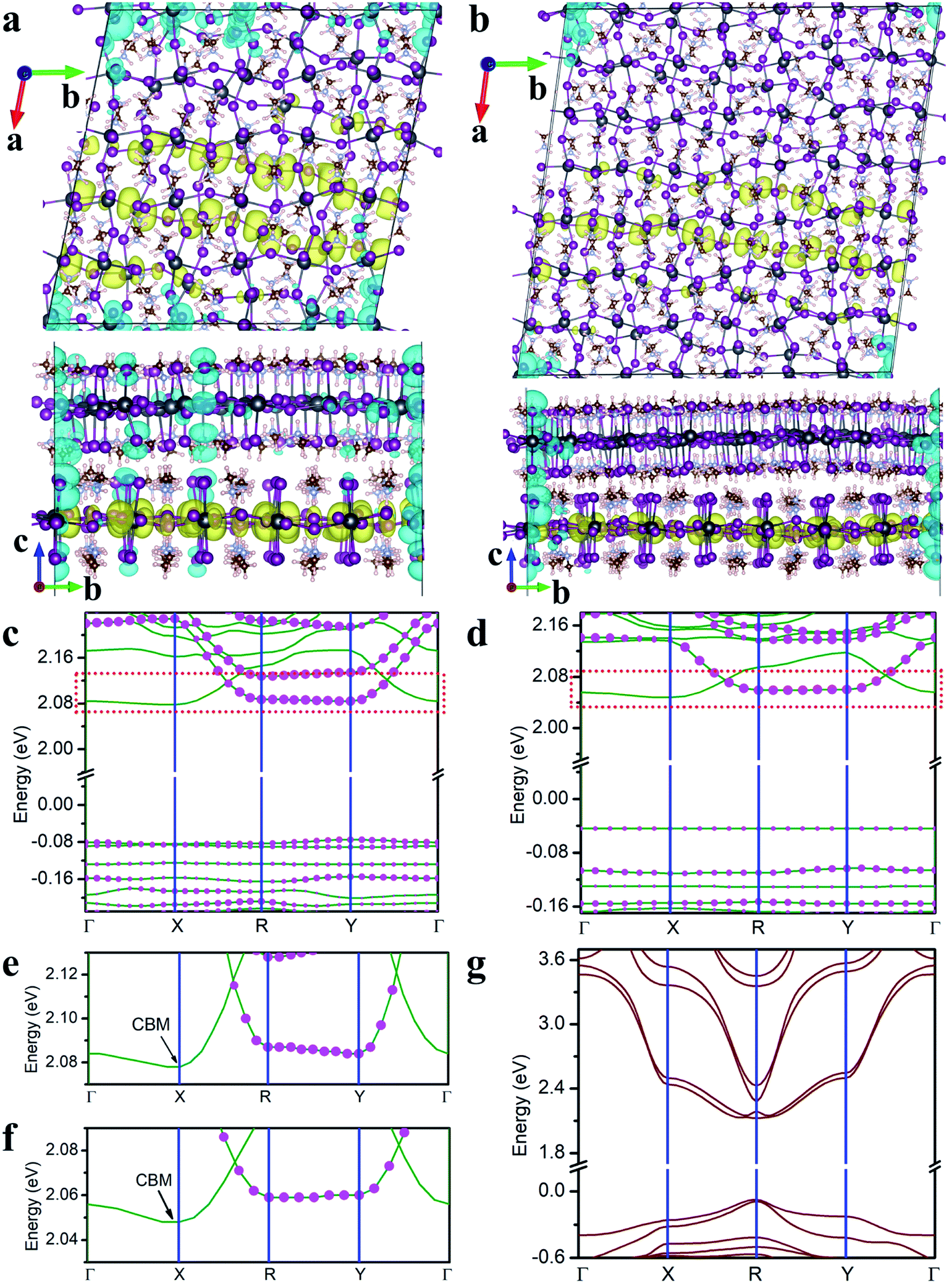 | ||
| Fig. 3 The charge density of the lowest energy exciton in twisted MA2PbI4 bilayer with θ = 11.3° (a) and θ = 8.1° (b). The hole and electron densities (iso-surface value set at 0.0001 e Å−3) are shown in cyan and yellow color, respectively. The single-particle band structure of twisted MA2PbI4 bilayer with θ = 11.3° (c) and θ = 8.1° (d) with the Fermi level set to zero. The relative contribution from the top layer is indicated by the size of pink dots in each band (the absence of the dots suggests no contribution from the top layer). The high-symmetry points in the Brillouin zone are labeled by Γ (0, 0, 0), X (0.5, 0, 0), Y (0, 0.5, 0), and R (0.5, 0.5, 0). (e and f) A blown-up view of the dashed box in (c) and (d). (g) The single-particle band structure of the non-twisted bilayer in the A stacking. | ||
We next analyze the compositions of CBM and VBM. The projected density of states in Fig. S2† indicates that CBM consists primarily of Pb 6p orbitals while VBM of I 5p orbitals. Furthermore, we find that CBM mainly originates from the bottom layer (Fig. 3e and f) while VBM shares contributions from both layers (Fig. 3c and d). Thus, I ions in both layers are responsible for the formation of the flat VBM band while Pb ions in the bottom layer contribute to more dispersive CBM. In other words, the interlayer I–I coupling, via both vdW interaction and H bonds, leads to the formation of the flat valence bands. In contrast, since CBM arises from the bottom layer, it exhibits a larger bandwidth due to the lack of interlayer Pb–Pb coupling.
The charge densities of the lowest energy exciton in both twisted MA2PbI4 bilayers are shown in Fig. 3a and b. It is found that the exciton becomes localized, in stark contrast to the non-twisted bilayers. Specifically, the hole is localized at the corner of the moiré supercell whereas the electron exhibits a striped distribution along b axis. The localized hole is shared by both layers while the electron is confined in the bottom layer; these features are consistent with the fact that VBM has contributions from both layers while CBM is primarily from the bottom layer. Hence, the lowest moiré excitons in the perovskite bilayers are of hybridized nature with a combination of intra- and inter-layer characteristics. Inspection of Fig. 3b reveals that the hole resides at the locations where the interlayer separation, measured by I–I distance, is quite small (Fig. S3†). This observation affirms the conclusion that the interlayer I–I interaction is responsible for the formation of flat VBM bands and the localization of the hole. The striped electron distribution can be rationalized from the band structure in Fig. 3c and d where the lowest conduction band is found to be nearly flat from Γ to X along a axis. Thus, the electron is localized in a direction with a striped distribution along b axis. Similar flat bands and charge density stripes were also observed in twisted germanium selenide bilayers.46 However, no moiré exciton was reported in the previous work. Lastly, we note that both the electron and hole are more localized in θ = 8.1° than in θ = 11.3° twisted bilayer, in line with the narrower bands in the former.
Previous first-principles study15 and experiments14,17 have reported the formation of localized moiré excitons in twisted TMD bilayers, such as MoS2/WS2. The interlayer Pb–Pb distance in MA2PbI4 bilayers is 9.1–10.4 Å, which is much larger than the interlayer Mo–W distance (6.1–6.7 Å) in MoS2/WS2 bilayers. Thus, the interlayer Pb–Pb coupling in MA2PbI4 bilayer is expected to be weaker than the interlayer Mo–W coupling in MoS2/WS2 bilayer. As a result, the electron distribution is less localized in MA2PbI4 bilayers than in MoS2/WS2 bilayers.15 On the other hand, the shortest interlayer I–I distance in MA2PbI4 bilayer is ∼2.7 Å, which is less than the shortest interlayer S–S distance (3.1 Å) in MoS2/WS2 bilayer, thanks to the formation of I–H hydrogen bonds. The stronger interlayer I–I coupling yields more localized hole density in twisted MA2PbI4 bilayers as compared to the twisted MoS2/WS2 bilayers.15 Furthermore, in contrast to TMDs, MA2PbI4 contains organic cations (MA) which can rotate freely47–50 and can thus modulate the moiré potential and moiré excitons. To illustrate this effect, we re-calculate the band structure and the exciton charge density of the twisted MA2PbI4 bilayer (θ = 11.3°) with a different orientation of MA cations (Fig. S4†). In this case, the MA cations in the top and bottom layers are perpendicular to each other, in contrast with the previous case (Fig. 3a) where the MA cations are parallel to each other (the previous case is energetically more stable). As shown in Fig. S4,† both the bandwidths and the exciton charge density change considerably as a result of the MA rotation. We thus demonstrated that the rotation of MA cations can indeed provide additional means in tuning moiré excitons.
Since the interlayer distance plays a crucial role on the formation of the flat bands and localization of moiré excitons in twisted MA2PbI4 bilayers, one would expect that external pressures could be effective in tuning the optoelectronic properties of twisted perovskite bilayers. To examine the pressure effect, we reduce the interlayer distances in the twisted MA2PbI4 bilayers by 0.3 Å while keeping their in-plane lattice parameters the same. The charge density of the lowest energy exciton as well as the single-particle band structure in the presence of the pressure are shown in Fig. 4. For θ = 11.3°, the VBM bandwidth is reduced from 9 meV in the absence of the pressure to 0 meV in the presence of the pressure and concomitantly, the hole becomes more localized (Fig. 4a). There is negligible change on the VBM bandwidth in θ = 8.1° bilayer because its bandwidth was already ∼0 meV in the absence of pressure. Furthermore, additional flat valence bands are formed in both bilayers under the pressure. The electron density, on the other hand, is only slightly affected by the pressure owing to the much larger interlayer Pb–Pb distances. We also examine the effects of the pressure on the non-twisted MA2PbI4 bilayer (in the stacking A). As shown in Fig. S5,† the lowest energy exciton remains delocalized at the top layer, as in the pressure-free case. The pressure has a negligible effect on the bandwidths of CBM and VBM in the non-twisted bilayer. In other words, the pressure is only effective in twisted bilayers where moiré potentials are present; by deepening the moiré potentials, the pressures can localize moiré excitons and flatten energy bands.
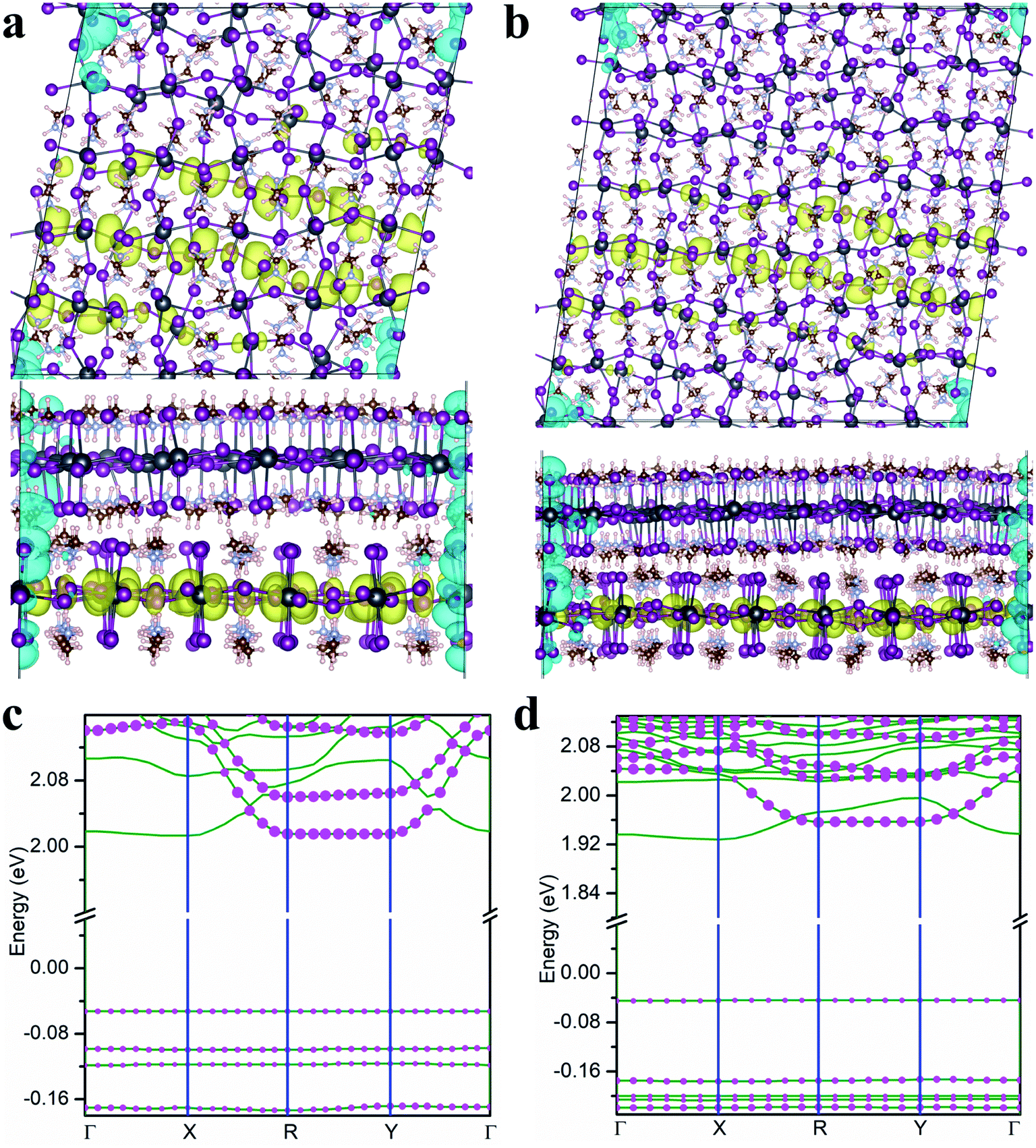 | ||
| Fig. 4 The charge density of the lowest energy exciton in the twisted MA2PbI4 bilayer with θ = 11.3° (a) and θ = 8.1° (b) under the pressure. The charge densities of the hole and electron (iso-surface value set at 0.0001 e Å−3) are displayed in cyan and yellow color, respectively. The single-particle band structure of the twisted MA2PbI4 bilayer with θ = 11.3° (c) and θ = 8.1° (d) under the pressure. The Fermi level is set to zero. | ||
Interlayer excitons are often more desirable in optoelectronic applications owing to their much longer lifetimes compared to intralayer excitons.51 The lowest moiré excitons in the twisted MA2PbI4 bilayers are a mixture of interlayer and intralayer characteristics with the electrons in the bottom layer and the holes spread in both layers. Next, we show that these hybridized excitons can be turned into interlayer excitons with a negative electric field normal to the layers. As illustrated in Fig. 5a, a negative electric field is predicted to lift the energy levels of the top layer and to lower the energy levels of the bottom layer. As a result, the type-II band alignment and thus interlayer excitons can be formed under appropriate negative fields. Fig. 5b displays the single-particle band structures of both twisted bilayers under an electric field of −6 V nm−1. In this case, VBM is attributed primarily to the top layer (with larger pink symbols) as opposed to both layers in the absence of the electric field. Thus, the hole is expected to be confined in the top layer while the electron remains in the bottom layer, forming an interlayer exciton. This is indeed what the exciton charge densities in Fig. 5c and d indicate. In addition to tuning the hybridization of the excitons, the electric field also affects the position and localization of the moiré excitons, illustrated in Fig. 5c and d. We also note that both the fundamental and optical bandgaps of the twisted bilayers can be lowered by the negative electric field, but the exciton binding energy remains roughly the same (Table S3†). Thus, electrostatic gating can be an effective means in tuning the optoelectronic properties of twisted perovskite bilayers.
 | ||
| Fig. 5 (a) Schematic diagram of band alignment under a negative electric field E. (b) The single-particle band structure of the twisted MA2PbI4 bilayer with θ = 11.3° (left) and θ = 8.1° (right) under an electric field of −6 V nm−1. The Fermi level is set to zero. The relative contribution from the top layer is indicated by the size of pink dots in each band. The charge density of the lowest energy exciton in the twisted MA2PbI4 bilayer with θ = 11.3° (c) and θ = 8.1° (d) under the electric field of −6 V nm−1. The charge densities of the hole and the electron (iso-surface value set at 0.0001 e Å−3) are shown in cyan and yellow color, respectively. | ||
Conclusions
In this work, we predict that twisted homobilayers of 2D RP perovskite MA2PbI4 can host moiré excitons and yield flat valence bands. Although the moiré potential in MA2PbI4 bilayers has the similar amplitude as TMD bilayers, the moiré excitons in MA2PbI4 bilayers exhibits unique and intriguing properties. Specifically, in twisted MA2PbI4 bilayers, the holes are localized in both layers, but the electrons exhibit a 1D striped distribution in a single layer. Moreover, nearly flat valence bands can be formed in twisted MA2PbI4 bilayers at larger twist angles than TMD bilayers. The relative ease in the flat band formation is attributed to the interlayer H bonds in MA2PbI4, which enhances the interlayer I–I coupling and deepens the moiré potential. External pressures can further increase the interlayer coupling and lead to more localized moiré excitons and flatter valence bands. Finally, we predict that the electrostatic gating can tune the degree of hybridization, energy, position and localization of moiré excitons in twisted MA2PbI4 bilayers. Our work lays the theoretical foundation for potential quantum optoelectronic applications of 2D perovskite heterostructures.Author contributions
G. L. designed the study, and L. Z. carried out calculations with the assistance of X. Z. G. L. supervised the research and wrote the manuscript with L. Z. All authors discussed the results.Conflicts of interest
The authors declare no conflict of interest.Acknowledgements
This work was supported by the NSF (DMR1828019) and the Army Research Office (W911NF1810473).References
- Y. Cao, V. Fatemi, S. Fang, K. Watanabe, T. Taniguchi, E. Kaxiras and P. Jarillo-Herrero, Nature, 2018, 556, 43–50 CrossRef CAS
.
- Y. Cao, V. Fatemi, A. Demir, S. Fang, S. L. Tomarken, J. Y. Luo, J. D. Sanchez-Yamagishi, K. Watanabe, T. Taniguchi, E. Kaxiras, R. C. Ashoori and P. Jarillo-Herrero, Nature, 2018, 556, 80–84 CrossRef CAS
- L. Liu, Y. Sun, X. Cui, K. Qi, X. He, Q. Bao, W. Ma, J. Lu, H. Fang, P. Zhang, L. Zheng, L. Yu, D. J. Singh, Q. Xiong, L. Zhang and W. Zheng, Nat. Commun., 2019, 10, 4472 CrossRef PubMed
- H. Baek, M. Brotons-Gisbert, Z. X. Koong, A. Campbell, M. Rambach, K. Watanabe, T. Taniguchi and B. D. Gerardot, Sci. Adv., 2020, 6, eaba8526 CrossRef CAS PubMed
- S. S. Sunku, G. X. Ni, B. Y. Jiang, H. Yoo, A. Sternbach, A. S. McLeod, T. Stauber, L. Xiong, T. Taniguchi, K. Watanabe, P. Kim, M. M. Fogler and D. N. Basov, Science, 2018, 362, 1153–1156 CrossRef CAS
- L. Yuan, B. Zheng, J. Kunstmann, T. Brumme, A. B. Kuc, C. Ma, S. Deng, D. Blach, A. Pan and L. Huang, Nat. Mater., 2020, 19, 617–623 CrossRef CAS PubMed
- R. Bistritzer and A. H. MacDonald, Proc. Natl. Acad. Sci. U. S. A., 2011, 108, 12233–12237 CrossRef CAS PubMed
- F. Wu, T. Lovorn, E. Tutuc and A. H. MacDonald, Phys. Rev. Lett., 2018, 121, 026402 CrossRef CAS PubMed
- X.-J. Zhao, Y. Yang, D.-B. Zhang and S.-H. Wei, Phys. Rev. Lett., 2020, 124, 086401 CrossRef CAS PubMed
- G. Chen, A. L. Sharpe, P. Gallagher, I. T. Rosen, E. J. Fox, L. Jiang, B. Lyu, H. Li, K. Watanabe, T. Taniguchi, J. Jung, Z. Shi, D. Goldhaber-Gordon, Y. Zhang and F. Wang, Nature, 2019, 572, 215–219 CrossRef CAS PubMed
- E. C. Regan, D. Wang, C. Jin, M. I. Bakti Utama, B. Gao, X. Wei, S. Zhao, W. Zhao, Z. Zhang, K. Yumigeta, M. Blei, J. D. Carlström, K. Watanabe, T. Taniguchi, S. Tongay, M. Crommie, A. Zettl and F. Wang, Nature, 2020, 579, 359–363 CrossRef CAS PubMed
- C. R. Dean, L. Wang, P. Maher, C. Forsythe, F. Ghahari, Y. Gao, J. Katoch, M. Ishigami, P. Moon, M. Koshino, T. Taniguchi, K. Watanabe, K. L. Shepard, J. Hone and P. Kim, Nature, 2013, 497, 598–602 CrossRef CAS PubMed
- E. M. Alexeev, D. A. Ruiz-Tijerina, M. Danovich, M. J. Hamer, D. J. Terry, P. K. Nayak, S. Ahn, S. Pak, J. Lee, J. I. Sohn, M. R. Molas, M. Koperski, K. Watanabe, T. Taniguchi, K. S. Novoselov, R. V. Gorbachev, H. S. Shin, V. I. Fal'ko and A. I. Tartakovskii, Nature, 2019, 567, 81–86 CrossRef CAS PubMed
- K. Tran, G. Moody, F. Wu, X. Lu, J. Choi, K. Kim, A. Rai, D. A. Sanchez, J. Quan, A. Singh, J. Embley, A. Zepeda, M. Campbell, T. Autry, T. Taniguchi, K. Watanabe, N. Lu, S. K. Banerjee, K. L. Silverman, S. Kim, E. Tutuc, L. Yang, A. H. MacDonald and X. Li, Nature, 2019, 567, 71–75 CrossRef CAS PubMed
- H. Guo, X. Zhang and G. Lu, Sci. Adv., 2020, 6, eabc5638 CrossRef CAS PubMed
- Y. Bai, L. Zhou, J. Wang, W. Wu, L. J. McGilly, D. Halbertal, C. F. B. Lo, F. Liu, J. Ardelean, P. Rivera, N. R. Finney, X.-C. Yang, D. N. Basov, W. Yao, X. Xu, J. Hone, A. N. Pasupathy and X. Y. Zhu, Nat. Mater., 2020, 19, 1068–1073 CrossRef CAS PubMed
- C. Jin, E. C. Regan, A. Yan, M. Iqbal Bakti Utama, D. Wang, S. Zhao, Y. Qin, S. Yang, Z. Zheng, S. Shi, K. Watanabe, T. Taniguchi, S. Tongay, A. Zettl and F. Wang, Nature, 2019, 567, 76–80 CrossRef CAS PubMed
- S. Brem, C. Linderälv, P. Erhart and E. Malic, Nano Lett., 2020, 20, 8534–8540 CrossRef CAS PubMed
- M. Koperski, K. Nogajewski, A. Arora, V. Cherkez, P. Mallet, J. Y. Veuillen, J. Marcus, P. Kossacki and M. Potemski, Nat. Nanotechnol., 2015, 10, 503–506 CrossRef CAS PubMed
- Y.-M. He, G. Clark, J. R. Schaibley, Y. He, M.-C. Chen, Y.-J. Wei, X. Ding, Q. Zhang, W. Yao, X. Xu, C.-Y. Lu and J.-W. Pan, Nat. Nanotechnol., 2015, 10, 497–502 CrossRef CAS PubMed
- Z. Wang, D. A. Rhodes, K. Watanabe, T. Taniguchi, J. C. Hone, J. Shan and K. F. Mak, Nature, 2019, 574, 76–80 CrossRef CAS PubMed
- A. L. Sharpe, E. J. Fox, A. W. Barnard, J. Finney, K. Watanabe, T. Taniguchi, M. A. Kastner and D. Goldhaber-Gordon, Science, 2019, 365, 605–608 CrossRef CAS PubMed
- J. Kang, J. Li, S.-S. Li, J.-B. Xia and L.-W. Wang, Nano Lett., 2013, 13, 5485–5490 CrossRef CAS PubMed
- Z. Song, X. Sun and L. Wang, J. Phys. Chem. Lett., 2020, 11, 9224–9229 CrossRef CAS PubMed
- M. H. Naik and M. Jain, Phys. Rev. Lett., 2018, 121, 266401 CrossRef CAS PubMed
- Z. Zhang, Y. Wang, K. Watanabe, T. Taniguchi, K. Ueno, E. Tutuc and B. J. LeRoy, Nat. Phys., 2020, 16, 1093–1096 Search PubMed
- X. Wu, M. T. Trinh and X. Y. Zhu, J. Phys. Chem. C, 2015, 119, 14714–14721 CrossRef CAS
- J. C. Blancon, A. V. Stier, H. Tsai, W. Nie, C. C. Stoumpos, B. Traoré, L. Pedesseau, M. Kepenekian, F. Katsutani, G. T. Noe, J. Kono, S. Tretiak, S. A. Crooker, C. Katan, M. G. Kanatzidis, J. J. Crochet, J. Even and A. D. Mohite, Nat. Commun., 2018, 9, 2254 CrossRef PubMed
- J. V. Passarelli, C. M. Mauck, S. W. Winslow, C. F. Perkinson, J. C. Bard, H. Sai, K. W. Williams, A. Narayanan, D. J. Fairfield, M. P. Hendricks, W. A. Tisdale and S. I. Stupp, Nat. Chem., 2020, 12, 672–682 CrossRef CAS PubMed
- L. Zhang, X. Zhang and G. Lu, J. Phys. Chem. Lett., 2020, 11, 6982–6989 CrossRef CAS PubMed
- D. Wang, B. Wen, Y.-N. Zhu, C.-J. Tong, Z.-K. Tang and L.-M. Liu, J. Phys. Chem. Lett., 2017, 8, 876–883 CrossRef CAS PubMed
- J.-C. Blancon, H. Tsai, W. Nie, C. C. Stoumpos, L. Pedesseau, C. Katan, M. Kepenekian, C. M. M. Soe, K. Appavoo, M. Y. Sfeir, S. Tretiak, P. M. Ajayan, M. G. Kanatzidis, J. Even, J. J. Crochet and A. D. Mohite, Science, 2017, 355, 1288–1292 CrossRef CAS PubMed
- J. Xi, I. Spanopoulos, K. Bang, J. Xu, H. Dong, Y. Yang, C. D. Malliakas, J. M. Hoffman, M. G. Kanatzidis and Z. Wu, J. Am. Chem. Soc., 2020, 142, 19705–19714 CrossRef CAS PubMed
- A. Wang, Y. Guo, Z. Zhou, X. Niu, Y. Wang, F. Muhammad, H. Li, T. Zhang, J. Wang, S. Nie and Z. Deng, Chem. Sci., 2019, 10, 4573–4579 RSC
- J. Guo, T. Liu, M. Li, C. Liang, K. Wang, G. Hong, Y. Tang, G. Long, S.-F. Yu, T.-W. Lee, W. Huang and G. Xing, Nat. Commun., 2020, 11, 3361 CrossRef PubMed
- Z. Tan, Y. Wu, H. Hong, J. Yin, J. Zhang, L. Lin, M. Wang, X. Sun, L. Sun, Y. Huang, K. Liu, Z. Liu and H. Peng, J. Am. Chem. Soc., 2016, 138, 16612–16615 CrossRef CAS PubMed
- D. Pan, Y. Fu, N. Spitha, Y. Zhao, C. R. Roy, D. J. Morrow, D. D. Kohler, J. C. Wright and S. Jin, Nat. Nanotechnol., 2021, 16, 159–165 CrossRef CAS PubMed
- H. Zhao, B. Wang, F. Liu, X. Yan, H. Wang, W. S. Leong, M. J. Stevens, P. Vashishta, A. Nakano, J. Kong, R. Kalia and H. Wang, Adv. Funct. Mater., 2020, 30, 1908691 CrossRef CAS
- X. Zhu, Z. Xu, S. Zuo, J. Feng, Z. Wang, X. Zhang, K. Zhao, J. Zhang, H. Liu, S. Priya, S. F. Liu and D. Yang, Energy Environ. Sci., 2018, 11, 3349–3357 RSC
- Y. Yang, F. Gao, S. Gao and S.-H. Wei, J. Mater. Chem. A, 2018, 6, 14949–14955 RSC
- P. Kang, W.-T. Zhang, V. Michaud-Rioux, X.-H. Kong, C. Hu, G.-H. Yu and H. Guo, Phys. Rev. B, 2017, 96, 195406 CrossRef
- G. Constantinescu, A. Kuc and T. Heine, Phys. Rev. Lett., 2013, 111, 036104 CrossRef PubMed
- I. Paradisanos, S. Shree, A. George, N. Leisgang, C. Robert, K. Watanabe, T. Taniguchi, R. J. Warburton, A. Turchanin, X. Marie, I. C. Gerber and B. Urbaszek, Nat. Commun., 2020, 11, 2391 CrossRef CAS PubMed
- S. Das, G. Gupta and K. Majumdar, Phys. Rev. B, 2019, 99, 165411 CrossRef CAS
- F. Wu, T. Lovorn and A. H. MacDonald, Phys. Rev. Lett., 2017, 118, 147401 CrossRef PubMed
- D. M. Kennes, L. Xian, M. Claassen and A. Rubio, Nat. Commun., 2020, 11, 1124 CrossRef CAS PubMed
- Y. Ren, I. W. H. Oswald, X. Wang, G. T. McCandless and J. Y. Chan, Cryst. Growth Des., 2016, 16, 2945–2951 CrossRef CAS
- L. Zhang, X. Zhang and G. Lu, J. Phys. Chem. Lett., 2020, 11, 2910–2916 CrossRef CAS
- L. Zhang and P. H. L. Sit, J. Phys. Chem. C, 2015, 119, 22370–22378 CrossRef CAS
- C. Motta, F. El-Mellouhi, S. Kais, N. Tabet, F. Alharbi and S. Sanvito, Nat. Commun., 2015, 6, 7026 CrossRef CAS PubMed
- P. Rivera, K. L. Seyler, H. Yu, J. R. Schaibley, J. Yan, D. G. Mandrus, W. Yao and X. Xu, Science, 2016, 351, 688–691 CrossRef CAS PubMed
Footnote |
| † Electronic supplementary information (ESI) available. See DOI: 10.1039/d1sc00359c |
| This journal is © The Royal Society of Chemistry 2021 |