 Open Access Article
Tracking the optical mass centroid of single electroactive nanoparticles reveals the electrochemically inactive zone†
Wenxuan
Jiang
 ,
Wei
Wei
 ,
Tinglian
Yuan
 ,
Shasha
Liu
 ,
Ben
Niu
 ,
Hui
Wang
 * and
Wei
Wang
 *
*
State Key Laboratory of Analytical Chemistry for Life Science, School of Chemistry and Chemical Engineering, Nanjing University, 210023, China. E-mail: huiwang520@nju.edu.cn; wei.wang@nju.edu.cn
First published on 13th May 2021
Abstract
The inevitable microstructural defects, including cracks, grain boundaries and cavities, make a portion of the material inaccessible to electrons and ions, becoming the incentives for electrochemically inactive zones in single entity. Herein, we introduced dark field microscopy to study the variation of scattering spectrum and optical mass centroid (OMC) of single Prussian blue nanoparticles during electrochemical reaction. The “dark zone” embedded in a single electroactive nanoparticle resulted in the incomplete reaction, and consequently led to the misalignment of OMC for different electrochemical intermediate states. We further revealed the dark zones such as lattice defects in the same entity, which were externally manifested as the fixed pathway for OMC for the migration of potassium ions. This method opens up enormous potentiality to optically access the heterogeneous intraparticle dark zones, with implications for evaluating the crystallinity and electrochemical recyclability of single electroactive nano-objects.
Introduction
Single nanoparticle electrochemistry is essential to reveal the nanoscale mechanism by the exposure of heterogeneous details such as size, shape, and surface defects, which would be otherwise hidden in an ensemble-averaged measurement. Uncovering the inherent structural and functional heterogeneity among individual particles could be treated as an effective approach to evaluate the practical property and optimize the performance of electrode materials for ionic batteries. There is no doubt that routine electrochemical measurements and numerous in situ characterization techniques such as X-ray diffraction and Raman spectroscopy have been utilized to access the overall electron accessibility of bulk materials at the ensemble level.1–3 It remains a challenge to evaluate the electrochemically inactive zones at the single nanoparticle level. Such capability is of particular interest when considering the inherent structural and functional heterogeneity among individual particles.4,5 Based on the optical signatures of single nanoparticles during the electrochemical events, numerous imaging techniques have been developed for resolving the nanoscale structure–activity of individual particles owing to their solvent compatibility, non-invasive nature and excellent sensitivity.6–12 We have recently demonstrated that the optical cyclic voltammograms of single LiCoO2 nanoparticles can be obtained via surface plasmon resonance microscopy.13 The lithiation and de-lithiation reversibly altered its dielectric constant and led to the optical intensity change. The time derivative of the single nanoparticle optical curve gave the ion transfer rate, i.e., current, of single nanoparticle. In order to take full advantage of the spatial resolution of optical microscopy, an edge-tracking method was recently proposed by Tao et al. to locate the edge of nanostructures optically, allowing for studying the electrochemical stress of single gold nanowire and the Pauli repulsion of graphene during electrochemical charging.14,15 The super-localization approaches combined with different optical techniques were also developed to monitor the centroid of electroactive entities during reactions,16–18 which is down to sub-diffraction limited resolution. The potential-dependent centroid revealed the detailed reaction mechanisms at the single nanoparticle level.However, these single nanoparticle studies often lie in a pre-assumption that the particular electroactive nanoparticle underwent a complete and effective reaction, i.e., the entire nanoparticle is accessible to electrons and ions. This pre-assumption may not be valid in practical systems. The identification of heterogeneous properties at the sub-particle level requires a combination of surface sensitive and high-resolution technique to uncover the heterogeneity in a well-defined nanoparticle. Several recent studies highlighted the incomplete reactions of individual Ag nanoparticles.19,20 Kanoufi et al. proposed the heterogeneous multiple-step conversion of AgX into metallic Ag nanoparticles with the formation of multiple inclusions in a single entity.21 Willets et al. studied the role of the surface oxide layers of single silver nanoparticles on the electrochemical reactions to visualize the effects of the partial oxide formation via dark-field scattering.20
Smart windows are based on electrochromic films, whose tunable optical properties stem from the electrochemical ion-insertion/-extraction reaction. Sambur et al. identified champion particles that tint the fastest and block the most radiation by watching single WO3 nanoparticles in a model smart window device.22 Recently, the study of Prussian blue (PB) and its analog related nanomaterials has drawn tremendous attention mainly owing to their excellent electrochromic properties.23–25 It has been well documented that an appropriate negative potential can efficiently reduce blue-colored PB to colorless Prussian white (PW) due to the reduction of Fe(III) and the insertion of potassium ions, accompanied with a dramatic change in the absorption spectrum in the visible range.26,27 Switching between positive and negative voltages makes the reversible conversion between PB and PW. The intermediate states mix with two components in different proportions. Ultrahigh stability and low cost for PB nanoparticles, clearly peculiar to noble metal-free inorganic coordinates, could be applied in potassium ion batteries and the catalytic substitution of natural and recombinant peroxidases.28–32 Furthermore, the extraordinary electrochromic characterization of this material provides the possibility of colorimetric labels in biotechnology and analytical science at nanoscale.33,34
In the present study, we introduced the dark-field imaging for determining the optical mass centroid (OMC) variation of single inorganic metal coordination nanoparticles during transition between different electrochemical states, which is attributed to the resonance elastic scattering. Prussian blue nanoparticles (PBNPs) were selected as a model coordinate material benefitted from their well-structured face-centered cubic structure synthesized via a conventional procedure,35 facilitating the interrogations on the correlation between electron accessibility and morphological crystallinity. Using a color or monochromic camera, the scattering light of numerous intermediate states from PB to PW nanoparticles during the redox reactions were captured. The patterns for individual particles were analyzed via 2-D Gaussian fitting36 for uncovering the characteristics of OMC, which corresponded to the extent of the electrochemical reaction of single entity. When the structure of PBNP is uniform, this ideal state of PB can be fully reduced to the PW state and the OMC of two states will coincide completely. When the interior structure of PBNP is inhomogeneous and some of the sub-particle portion is not accessible to the ions and electrons, one should observe the misalignment of OMC for different intermediate states during the redox reaction, leading to a OMC movement trajectory induced by the ion migration. This approach highlights the structural–activity correlation of PB nanoparticles and demonstrates unambiguous quantitative information during electrochemical process dynamically.
Results and discussion
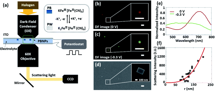
Herein, we performed a dark-field imaging technique to uncover the electrochromic property of single PB nanoparticles modulated by the electrochemical voltage, as shown in Fig. 1a. As a light source, a halogen lamp was equipped with conventional dark-field microscopy (DFM), which included an oil-immersed condenser with a high numerical aperture (NA = 1.20–1.43). The as-prepared PBNPs with cuboid morphology were deposited on an indium tin oxide (ITO)-coated glass slide to serve as a working electrode. The scattered light was collected by a 60× water-immersed objective (NA = 1.0) to generate the image in a color or monochromatic camera. Specific details regarding the synthesis and the optical configuration are described in experimental, and the comprehensive characterizations of the as-prepared PNBPs are shown in Fig. S1.† A broad extinction band from 500 to 900 nm with a strong optical extinction peak around 740 nm was observed for PBNPs in the UV-Vis spectra (Fig. S1a†), corresponding to the energy of the metal-to-metal charge transfer between Fe(III) and Fe(II) ions through the cyanide bridge.27,37 From the scanning electron microscopic (SEM) image of the as-synthesized PB nanostructures shown in Fig. S1b,† it is revealed that the morphology was all in the well-structured cubic shape. Furthermore, the crystallography and phase information of PBNPs were acquired via X-ray diffraction (XRD) measurements for corroborating this face-centered cubic structure with a lattice parameter of 10.15 Å (see the ESI, Fig. S1c†), which is consistent with literature.38–40For the electrochromic property, the blue-colored PB can be reduced to the colorless Prussian white (PW), and this process is highly reversible and reproducible by switching between positive and negative voltages.26,27 We performed the electrochemical modulation with a polydimethylsiloxane (PDMS) chamber (1 mm thickness) containing the electrolyte (0.1 M KNO3 solution) placed between two ITO slides (see the ESI, Fig. S2†). The dark-field scattering image of single PBNPs appeared red at 0 V, and turned to green after reducing to the PW state by applying a negative voltage (−0.3 V) (Fig. 1b and c and Movie S1†). The red color of the PB state can be attributed to the resonance elastic scattering of individual coordinate nanoparticles, as a result of the electronic transition between Fe(III) and Fe(II) ions. The corresponding in situ SEM image in Fig. 1d revealed the neat cubic shape of individual PBNPs deposited on the ITO slide. The first-order derivative of the DFM intensity curve showed two main peaks located at the specific voltages of PW oxidation and PB reduction (Fig. S1d†), which was consistent with the traditional cyclic voltammetry of PBNPs in our previous study.26,41Fig. 1e shows the normalized scattering spectra of PB and PW states for the same nanoparticle (Fig. 1b–d, insets), revealing the variation of scattering spectra at different voltages. A broad peak with the maximum scattering wavelength near 700 nm for the PB state at 0 V, which is in agreement with the extinction spectrum from UV-vis measurements, supports that the red color is a result of the resonant elastic scattering. To investigate the sensitivity, dark-field images and the corresponding SEM images of the very same individual PBNPs were collected and compared (Fig. 1f and more details in the ESI Fig. S4†). The relative intensity of single nanoparticles in Fig. 1f is normalized by subtracting the background intensity of the dark-field scattering. It was found that a commercial dark-field microscope with a conventional halogen lamp was capable of visualizing single PBNPs as small as 80 nm.
The dark field imaging technique was frequently adopted to study two main systems: one is plasmonic nanomaterials, typically composed of silver or gold, which collect the scattering light from the oscillation of the conducting electrons;6,11,42–44 and another one is high refractive index dielectric or semiconductor nanoparticles for use in nano-photonics, such as crystalline silicon.45,46 The present study uncovers a promising strength of dark-field scattering microscopy for studying ion-storage nanomaterials with implications for ionic batteries.
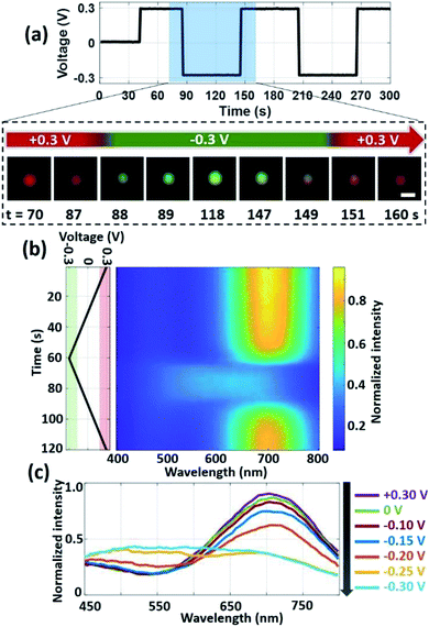
By modulating the square-wave voltage, the time-lapsed DFM images of single PBNP in Fig. 2a and Movie S1† showed gradual transition in the scattering color, which was attributed to the dynamic process of the redox reaction. It is well known that PW appears colorless to the naked eye and do not absorb any visible light. However, in our measurement, the green round dot was observed after electrochemical reduction. The scattering spectrum of the PW state further revealed a broad scattering band covering 450–750 nm. To uncover the essence of the change mentioned above, the voltage-dependent scattering spectra of one PBNP during electrochemical cycling were captured and mapped in Fig. 2b. The scattering spectrum of PBNP has a broad absorption peak with a central wavelength near 700 nm, and stabilizes in the positive voltage range. The normalized intensity of the main peak at the wavelength of maximum absorbance known for this material (700 nm) decreases gradually at the negative direction of voltage sweeping from 0 V to −0.3 V, and eventually disappears at −0.25 V accompanied by a slight increase near 550 nm. When the voltage sweeps back to positive, the scattering spectrum recovers. Fig. 2c compares the scattering spectrums at several specific voltages to show the variation in the main peak intensity and position, and provide important insights into the intermediate details during voltage modulation.
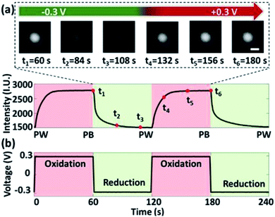
To elaborate the kinetics of electrochemical transition between PB and PW, the monochromic optical readout of single nanoparticle in Fig. 3a and Movie S2† could extract the scattering intensity change of pure PB component and filter out the interference from PW. A monochromic CCD camera combined with a 700 nm long-pass filter was used to replace the color camera. The corresponding square-wave voltage with two complete cycles shown in Fig. 3b illustrates the long-time intervals between two states for ensuring the effective mutual transition between PB and PW states. The scattered image of individual PBNPs exhibited round dots, which can be subsequently fitted by a 2-D Gaussian function to ascertain the coordinates of optical mass centroid (OMC). The complete definitions of the above parameter for single nanoparticles, OMC, is explained in the ESI S2† and Fig. 4 (we have discussed it below.). It was directly influenced by voltage modulation and the trend was almost same as that of intensity (Fig. 3b).
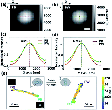
For the real-time tracking of the variation of OMC, we applied 2-D Gaussian fitting to a series of time-lapsed dark-field images of PB and PW states that are continuously recorded during the voltage cycling (Fig. 4a and b), and intensity profiles across the pattern along the x and y directions are displayed in Fig. 4c and d (red and green lines). Polystyrene nanoparticles (PSNPs) with a diameter of 500 nm were added to the system and attached to the substrate for drift correction (more details in the ESI Fig. S5†). The trajectory of OMC for the single PB entity reveals a back-and-forth behaviour during voltage cycling in 2 min (Fig. 4e) among the x–y plane, which was externally manifested by the change of space coordinates for the peak of Gaussian distribution. To validate that the tracking result was not induced by the optical artifacts or mechanical drift, we rotated the orientation of the sample by 90 degrees and mapped the real-time trajectories of OMC for the same PBNP before and after rotation (Fig. 4e).
The direction of trajectories for this particular single PBNP showed the expected change with different orientations, and the average displacement of OMC for this same PBNP from the PB to PW state was 80.8 nm. The time interval between each adjacent points in this figure was 1 s. When the voltage swept back to the negative side, the OMC returned to the initial point along the same pathway to display the high reversibility modulated by voltage. We tracked 47 PBNPs, and all of them revealed displacements of OMC in Fig. S6.†
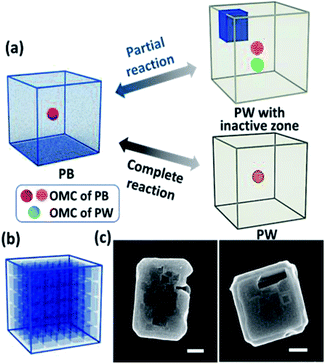
The misalignment of OMCs for different states in one redox cycle can be attributed to the electrochemical inactive zone in one PB nanoparticle. Fig. 5a illustrates the OMC variation for two different extents of the PB redox reaction. If we assume that the structure of PBNP is uniform, this ideal state of the entity can be fully reduced to PW and the OMC of two states will coincide completely. However, the interior structure of the as-synthesized PBNPs is heterogeneous and leads to the misalignment of OMC for different intermediate states during the redox reaction. From the XRD pattern of the PBNPs shown in Fig. S1c,† the crystallite size was estimated as 110.9 nm for the (200) face and 66.7 nm for the (220) face with the Scherrer equation. Since the particle size obtained from SEM images is about several times larger than the crystallite size estimated from XRD, it is suggested that the as-synthesized PBNPs are polycrystalline.
To further prove our demonstration and explore the interior structure of individual PBNPs, 0.01 M Na2S was subsequently added as a corrosion agent to reduce the Fe(III) in PB structures (Fig. 5b and c). The SEM images of single PBNPs after the erosion of the Na2S aqueous solution (Fig. 5c) clarified that a single cubic-shaped PB mesocrystal was formed by the oriented aggregation of small nanocrystals, as illustrated in Fig. 5b. These PB mesocrystals have small defects due to the dislocation and minor cavities formed during the crystallization process.47 The inactive zone of this asymmetric structure can be used to explain the misalignment of OMC for different electrochemical intermediate states presented in Fig. 4, and this regularity holds true for most PBNPs we measured. The OMC tracking result and the corresponding SEM image of another PB nanoparticle are shown in Fig. S7† to tell the same story as Fig. 4. The pattern of individual PW nanoparticle in Fig. 1c is a further evidence for this conclusion, which can be considered a two-component entity including green and red scattering lights corresponding to PW and inactive PB.
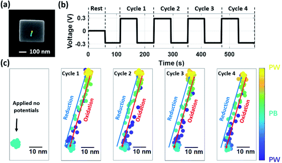
To verify the stability of individual PB nanoparticles, the periodic potential was applied and the trajectories of OMC in each cycle are plotted in Fig. 6. During the initial period of about 60 s, no potential was applied, and the OMC of PBNPs did not shift significantly. This result further proves that the observed OMC displacement is reliable. In the next four cycles, OMC moves from top to bottom at the oxidation potential, and moves back to the original position from bottom to top at the reduction potential. All the observed potential depended current curves are shown in ESI S7.† The tracking results of four cycles were highly reversible and reproducible during the transition between PB and PW states. Movie S3† shows the time-lapsed dark-field images of a PB nanoparticle during the cyclic square-wave voltage, and the real-time tracking of the OMC simultaneously. We attributed this observation to the fixed pathway in an individual PB crystal including the electrochemical inactive zones such as lattice defects in the same entity for the migration of potassium ions. The characterization of OMC variation for different PBNPs exhibits heterogeneity, which is closely related to the random distribution of electrochemical inactive zones embedded in single entity.
Conclusions
In summary, we have demonstrated the voltage-dependent dark-field imaging of the electrochromic property for noble metal-free inorganic coordinates, Prussian blue nanoparticles, based on the resonance elastic scattering. The gradual transition from PB to PW modulated by the voltage of a particular waveform was examined by the scattering spectrum, which was externally manifested as the color variance in dark-field images. The voltage dependence has been exploited to dynamically map the accurate coordinates of OMC at the single-nanoparticle level. It allows us to reveal the heterogeneous electroactivity within one PB entity. In particular, we uncovered the internal mechanism of OMC variation, which was attributed to the partial reaction during the highly reversible and reproducible switching of two states, and revealed the electrochemical inactive zones in single nanoparticle. The highly reversible and reproducible OMC tracking results in different electrochemical cycles uncovered the fixed pathway in an individual PB crystal for the migration of potassium ions. We further observed that the dark zones such as lattice defects may push the choice of pathway for ions in the same entity, which was further verified by SEM images. By taking PBNP as a model material with ultrahigh stability, the present method opens up enormous possibility to evaluate the crystallinity and electrochemical recyclability by accessing these heterogeneous inactive zones. Furthermore, it produces the prospect of a new approach to decipher the intraparticle migration pathway and diffusion of cations and electrons from the OMC of the entire nanoparticle, and brings inspiring details of internal mechanism to light for fundamental electrochemistry study and practical applications in electrochromic materials and ion batteries.Data availability
The datasets supporting this article have been uploaded as part of the supplementary material.Author contributions
W. Jiang and W. Wang designed the research and analyzed the data. W. Jiang and H. Wang wrote the manuscript. W. Jiang performed the experiments. W. Wei assisted to prepare PB samples for electrochemical experiments. W. Wei, S. Liu and T. Yuan helped to discuss the results. B. Niu helped to perform part of the additional experiment. W. Wang conceived and supervised this research.Conflicts of interest
There are no conflicts to declare.Acknowledgements
We thank the National Natural Science Foundation of China (Grants 21925403, 21904062 and 21874070), and the Excellent Research Program of Nanjing University (Grant ZYJH004) for financial support.References
- Y.-F. Huang, P. J. Kooyman and M. T. M. Koper, Nat. Commun., 2016, 7, 12440 CrossRef CAS PubMed.
- P. Vermeulen, H. J. Wondergem, P. C. J. Graat, D. M. Borsa, H. Schreuders, B. Dam, R. Griessen and P. H. L. Notten, J. Mater. Chem., 2008, 18, 3680–3687 RSC.
- G. Zhang, T. Xiong, L. He, M. Yan, K. Zhao, X. Xu and L. Mai, J. Mater. Sci., 2017, 52, 3697–3718 CrossRef CAS.
- T. J. Anderson and B. Zhang, Acc. Chem. Res., 2016, 49, 2625–2631 CrossRef CAS PubMed.
- M. V. Mirkin, T. Sun, Y. Yu and M. Zhou, Acc. Chem. Res., 2016, 49, 2328–2335 CrossRef CAS PubMed.
- C. M. Hill and S. Pan, J. Am. Chem. Soc., 2013, 135, 17250–17253 CrossRef CAS PubMed.
- Y. Fang, H. Wang, H. Yu, X. Liu, W. Wang, H.-Y. Chen and N. Tao, Acc. Chem. Res., 2016, 49, 2614–2624 CrossRef CAS PubMed.
- B. S. Hoener, S. R. Kirchner, T. S. Heiderscheit, S. S. E. Collins, W.-S. Chang, S. Link and C. F. Landes, Chem, 2018, 4, 1560–1585 CAS.
- W. Wang, Chem. Soc. Rev., 2018, 47, 2485–2508 RSC.
- P. Saha, J. W. Hill, J. D. Walmsley and C. M. Hill, Anal. Chem., 2018, 90, 12832–12839 CrossRef CAS PubMed.
- K. Wonner, M. V. Evers and K. Tschulik, J. Am. Chem. Soc., 2018, 140, 12658–12661 CrossRef CAS PubMed.
- F. T. Patrice, K. Qiu, Y.-L. Ying and Y.-T. Long, Annu. Rev. Anal. Chem., 2019, 12, 347–370 CrossRef PubMed.
- D. Jiang, Y. Jiang, Z. Li, T. Liu, X. Wo, Y. Fang, N. Tao, W. Wang and H.-Y. Chen, J. Am. Chem. Soc., 2017, 139, 186–192 CrossRef CAS PubMed.
- H. Wang, X. Shan, H. Yu, Y. Wang, W. Schmickler, H. Y. Chen and N. Tao, Angew. Chem., 2017, 129, 2164–2167 CrossRef.
- H. Wang, X. Shan, H.-Y. Chen and N. Tao, Nano Lett., 2017, 17, 236–241 CrossRef CAS PubMed.
- N. Zou, G. Chen, X. Mao, H. Shen, E. Choudhary, X. Zhou and P. Chen, ACS Nano, 2018, 12, 5570–5579 CrossRef CAS PubMed.
- T. Liu, S. Liu, W. Jiang and W. Wang, ACS Nano, 2019, 13, 6279–6286 CrossRef CAS PubMed.
- K. A. Willets, ACS Nano, 2019, 13, 6145–6150 CrossRef CAS PubMed.
- S. M. Oja, D. A. Robinson, N. J. Vitti, M. A. Edwards, Y. Liu, H. S. White and B. Zhang, J. Am. Chem. Soc., 2017, 139, 708–718 CrossRef CAS PubMed.
- V. Sundaresan, J. W. Monaghan and K. A. Willets, J. Phys. Chem. C, 2018, 122, 3138–3145 CrossRef CAS.
- J.-F. Lemineur, J.-M. Noel, A. Courty, D. Ausserre, C. Combellas and F. Kanoufi, J. Am. Chem. Soc., 2020, 142, 7937–7946 CrossRef CAS PubMed.
- R. C. Evans, A. Ellingworth, C. J. Cashen, C. R. Weinberger and J. B. Sambur, Proc. Natl. Acad. Sci. U. S. A., 2019, 116, 12666–12671 CrossRef CAS PubMed.
- D. Ellis, M. Eckhoff and V. Neff, J. Phys. Chem., 1981, 85, 1225–1231 CrossRef CAS.
- K. Itaya, K. Shibayama, H. Akahoshi and S. Toshima, J. Appl. Phys., 1982, 53, 804–805 CrossRef CAS.
- C. Zhang, Y. Xu, M. Zhou, L. Liang, H. Dong, M. Wu, Y. Yang and Y. Lei, Adv. Funct. Mater., 2017, 27, 1604307 CrossRef.
- D. Jiang, L. Sun, T. Liu and W. Wang, Anal. Chem., 2017, 89, 11641–11647 CrossRef CAS PubMed.
- M. B. Zakaria and T. Chikyow, Coord. Chem. Rev., 2017, 352, 328–345 CrossRef CAS.
- D. Su, A. McDonagh, S.-Z. Qiao and G. Wang, Adv. Mater., 2017, 29, 1604007 CrossRef PubMed.
- M. A. Komkova, E. E. Karyakina and A. A. Karyakin, J. Am. Chem. Soc., 2018, 140, 11302–11307 CrossRef CAS PubMed.
- D. Su, M. Cortie, H. Fan and G. Wang, Adv. Mater., 2017, 29, 1700587 CrossRef PubMed.
- D. Su, M. Cortie and G. Wang, Adv. Energy Mater., 2017, 7, 1602014 CrossRef.
- X. Tang, H. Liu, D. Su, P. H. L. Notten and G. Wang, Nano Res., 2018, 11, 3979–3990 CrossRef CAS.
- M. Shatruk, A. Dragulescu-Andrasi, K. E. Chambers, S. A. Stoian, E. L. Bominaar, C. Achim and K. R. Dunbar, J. Am. Chem. Soc., 2007, 129, 6104–6116 CrossRef CAS PubMed.
- Z. Qin, Y. Li and N. Gu, Adv. Healthcare Mater., 2018, 7, 1800347 CrossRef PubMed.
- X. L. Wu, M. H. Cao, C. W. Hu and X. Y. He, Cryst. Growth Des., 2006, 6, 26–28 CrossRef CAS.
- H. Cang, A. Labno, C. Lu, X. Yin, M. Liu, C. Gladden, Y. Liu and X. Zhang, Nature, 2011, 469, 385–388 CrossRef CAS PubMed.
- B. Kong, C. Selomulya, G. Zheng and D. Zhao, Chem. Soc. Rev., 2015, 44, 7997–8018 RSC.
- A. L. Patterson, Phys. Rev., 1939, 56, 978–982 CrossRef CAS.
- C. Wang, L. Zhang, Z. Guo, J. Xu, H. Wang, H. Shi, K. Zhai and X. Zhuo, Electroanalysis, 2010, 22, 1867–1872 CrossRef CAS.
- U. Holzwarth and N. Gibson, Nat. Nanotechnol., 2011, 6, 534 CrossRef CAS PubMed.
- W. Wei, T. Yuan, W. Jiang, J. Gao, H.-Y. Chen and W. Wang, J. Am. Chem. Soc., 2020, 142, 14307–14313 CrossRef CAS PubMed.
- Y. Li, C. Jing, L. Zhang and Y.-T. Long, Chem. Soc. Rev., 2012, 41, 632–642 RSC.
- J. Olson, S. Dominguez-Medina, A. Hoggard, L.-Y. Wang, W.-S. Chang and S. Link, Chem. Soc. Rev., 2015, 44, 40–57 RSC.
- H. Sun, Z. H. Wang and Y. He, ACS Nano, 2019, 13, 11334–11342 CrossRef CAS PubMed.
- J. C. Ginn, I. Brener, D. W. Peters, J. R. Wendt, J. O. Stevens, P. F. Hines, L. I. Basilio, L. K. Warne, J. F. Ihlefeld, P. G. Clem and M. B. Sinclair, Phys. Rev. Lett., 2012, 108, 097402 CrossRef PubMed.
- U. Zywietz, A. B. Evlyukhin, C. Reinhardt and B. N. Chichkov, Nat. Commun., 2014, 5, 3402 CrossRef PubMed.
- H. Cölfen and M. Antonietti, Angew. Chem., Int. Ed., 2005, 44, 5576–5591 CrossRef PubMed.
Footnote |
| † Electronic supplementary information (ESI) available: Materials and methods, characterizations of as-synthesis PB nanoparticles, determination of scattering intensity and equivalent radius for individual PBNPs, statistical analysis of OMC displacement between PB and PW state for individual entities and the reversible trajectory of OMC for single PBNP and description of movies. See DOI: 10.1039/d1sc01623g |
| This journal is © The Royal Society of Chemistry 2021 |

