 Open Access Article
Creative Commons Attribution 3.0 Unported Licence
Integrated co-axial electrospinning for a single-step production of 1D aligned bimetallic carbon fibers@AuNPs–PtNPs/NiNPs–PtNPs towards H2 detection†
Keerthi G.
Nair
,
Ramakrishnan
Vishnuraj
and
Biji
Pullithadathil
 *
*
Nanosensor Laboratory, PSG Institute of Advanced Studies, Coimbatore 641004, Tamil Nadu, India. E-mail: bijuja123@yahoo.co.in
First published on 28th October 2021
Abstract
One dimensional (1D) nanostructures such as nanorods, nanowires, nanotubes and nanofibers have aroused great attention owing to their exceptional properties like high surface-to-volume ratio and excellent electron and thermal transport and also act as interconnects during the fabrication of nanoscale devices. In this work, one dimensional aligned carbon nanofibers (CFs)@AuNPs–PtNPs/NiNPs–PtNPs have been developed via a single step co-axial electrospinning integrated with in situ photo-reduction. The carbon nanofibers with in situ functionalized bimetallic nanoparticles possessed a well-defined core–shell structure with carbon nanofibers (CFs) as the core and AuNPs–PtNPs/NiNPs–PtNPs as the surface anchored heterojunctions. Homogeneously distributed AuNPs–PtNPs/NiNPs–PtNPs, which are identified as chemical sensitizers, trigger the dissociation of H2 through the spillover effect, by successive diffusion of the H+ on the carbon nanofiber surface, thereby altering the entire surface of the CFs into reaction sites for H2. Aligned core–shell CFs@NiNPs-PtNPs possessed high sensitivity of 124% (v/v) at room temperature compared to aligned core–shell CFs@PtNPsNPs (52%) and aligned core–shell CFs@AuNPs–PtNPs (65%), which may be due to the high catalytic adsorption and desorption properties of Ni and Pt towards hydrogen gas. Moreover, co-axially aligned CF@NiNP–PtNP based sensor also demonstrates outstanding selectivity towards hydrogen compared to other gases like ammonia, ethanol, hydrogen sulphide, and acetone with excellent long-term stability. In addition, hydrogen adsorption kinetics of the co-axially aligned CF@NiNP–PtNP based sensor was verified theoretically with an adsorption rate constant of 0.42 which is comparable to the experimental value (0.38) of adsorption rate constant. The potential suitability of the co-axially aligned CF@NiNP–PtNP based sensor towards H2 at room temperature for real time applications has also been demonstrated.
1. Introduction
Hydrogen is considered as the future clean energy fuel and is widely used in numerous industries, such as petrochemical refineries, coolants, chemical synthesis, semiconductors, fuel cells, aerospace, automobile and as energy carriers in nuclear fusion power plants.1,2 Over the last decade, there has been growing research interest in the use of hydrogen as a zero-emission fuel in automotive applications. H2 as a fuel has already found its potential and is commercially feasible in markets comprising trucks powered by fuel cells and stationary power systems. For the effective deployment of hydrogen as an alternative fuel, it is very significant to develop the infrastructure of the hydrogen market carefully and efficiently. Leakage of hydrogen is a serious concern since it could lead to disastrous consequences, and may cause highly damaging explosions even on the laboratory scale. Therefore, deployment of H2 detectors is necessary in all such applications, mainly due to its colorless, tasteless and odorless nature. Consequently, efficient monitoring of trace level concentration of hydrogen has become critical. Therefore, hydrogen sensors developed with the parameters of sensitivity, speed, accuracy and reliability are in high demand for storage, production and usage of this forthcoming clean energy carrier.3 Buttner et al. have summarized the most significant requirements for H2 sensors in market, which include the H2 measurement in the range of 0.1–10% at an operating temperature below 80 °C, as per the target conditions set by the U.S. Department of Energy (DOE) in 2007.4 In this scenario, developing rapid and stable H2 sensors working at room temperature with a broad range of detection is crucial for early hazard prevention before the hydrogen-powered systems are widely exploited. Hydrogen based gas sensors were developed conventionally using numerous semiconducting metal oxides. However, semiconductor based H2 sensors need a high working temperature of 150–400 °C to accomplish high sensitivity and possess poor selectivity towards H2 gas.5 Recently, gas sensors based on 1D carbon materials, such as carbon nanofibers (CFs)6 and carbon nanotubes (CNTs),7 have gained considerable importance as ideal candidates for carbon nanostructure based sensors towards room temperature detection of H2 owing to their high surface to volume ratio and directed charge transport properties. Such carbon nanostructures can also be easily functionalized with noble metals or bimetals, leading to improved gas sensor performance.8 However, only a few reports are available on carbon nanofiber based gas sensors compared to CNT based gas sensors. Also, compared to quantum dots (0D), 1D carbon nanostructures with reduced dimensionality have demonstrated improved electrical properties, which might be due to three aspects: (i) the 1D carbon nanostructures have larger specific surface areas than quantum dots; (ii) 1D carbon nanostructures provide a direct electron transport pathway and thus reduce the electrical resistance, while the electrical resistance of quantum dots is typically high due to the presence of grain boundaries; (iii) 1D carbon nanostructures have brilliant abilities to be assembled into oriented structures, which would be favorable for the improvement in device performances, where the anisotropic formation is a key factor for the development of the oriented structure.9 The production of CNFs is generally carried out by methods such as electrospinning, CVD, templated synthesis, hydrothermal synthesis, catalytic hydrogenation, etc.10,11 Carbon nanofibers produced by electrospinning are simple, effective, versatile, scalable, and a low-cost technique that has been employed to fabricate 1D nanofibers.12 Co-axial electrospinning is found to be an effective method to produce core–shell type nanofibers which is a low-cost and continuous production method capable of nanofiber alignment.13 Aligned electrospun nanofibers have drawn enormous attention in the fields of sensors, drug delivery, tissue engineering, photoelectric devices, supercapacitors and blood vessel engineering since these applications entail highly ordered and well-aligned architectures in addition to the anisotropy and enhanced performance.14–16Functionalization of carbon nanostructures with platinum, palladium nanoparticles (NPs) or bimetallic nanoparticles is well-known for H2 gas detection since these catalytic NPs stimulate the reaction through dissociation of hydrogen molecules into hydrogen atoms. Bimetals are well recognized due to their synergetic effects. Bimetallic nanomaterials have four plausible types of mixing patterns between the two metals; they are (i) core–shell structures, (ii) sub-cluster segregated, (iii) homogeneously mixed alloys and (iv) multi-shell nanoalloys.17 Recently, trace level detection of hydrogen was discussed using catalytically active Pt-covered Pd nanowires and Pt–Pd/rGO.18 Even though Pt is a notable H2 sensing material, which helps in H2 dissociation at the exterior, forming Pt–H, compared to Pd, it remains on the exterior surfaces instead of dispersing into the bulk. Therefore, carbon nanostructures functionalized with PtNPs displayed better recovery of H2 sensors than Pd based sensors. Lately, Baro et al. described the consequence of NP distribution over graphene wrapped CNTs which displayed 42.8% sensitivity towards 4% of H2 at RT.19 It was noticeable that high loading of catalytic PtNPs on the carbon support diminishes the activity of the nanocatalyst and hence the sensor performance. Our earlier work has explored the bimetallic Au–PtNPs over CFs synthesized via a wet chemical route to sense H2 gas.20 The CFs with AuNPs–PtNPs upgraded the response time of the sensor in comparison with the monometallic PtNPs on CFs. Though CFs@AuNPs–PtNPs displayed exceptional H2 sensing properties and cost reduction, the multi-step fabrication process was found to be its limitation for mass production. In addition, less-PtNP functionalized carbon support might be more economical and advantageous with improved sensitivity without much shift in the base-resistance. Less-platinum based carbon nanofibers synthesized via a two-step method, electrospinning and chemical reduction, on a flexible substrate for room temperature hydrogen gas detection were reported in our previous report.21 Though incorporation of less-Pt based low-cost bimetallic systems over CFs on flexible substrates improved the sensor characteristics, for real-time applications, easy fabrication methods with improved sensor performance are more desirable. Therefore, for the real-time implementation of these sensors, the fabrication process must be easy and suitable for mass production. Recently, researchers have tried to reinforce on-chip fabrication of sensor devices, but such approaches were found to involve multi stage processes, which results in practical issues, a fact which hampers their mass production.22 Such difficulties might be overcome by single stage development of aligned core–shell type hybrid CFs with metals/bimetals over the CFs using the coaxial electrospinning process. However, there are no reports on single step fabrication of carbon nanofiber@metal/bimetal-based hybrid heterojunctions based on co-axial electrospinning with in situ photo reduction for room temperature H2 gas sensor applications.
In this investigation, we have demonstrated a single-step fabrication strategy based on co-axial electrospinning with in situ photo-reduction aimed at the production of aligned 1D CF@AuNP-PtNP/NiNP–PtNP based heterojunction nanofibers. The surface catalysis related to the noble metal/bimetal (PtNPs, AuNPs–PtNPs and NiNPs–PtNPs) shell layers and carbon nanofibers as core layers leads to an exhaustive understanding of the mechanism of gas–material interactions at the interfaces which was further verified by analyzing their in situ electron-transport properties. In addition, a prototype device based on the co-axially aligned CF@NiNP–PtNP based sensor was demonstrated for hydrogen gas detection. This study might furnish significant information about the selection of advanced sensor materials for room temperature H2 gas sensor devices with enhanced sensor performance and process conditions with improved selectivity which favour mass production of H2 sensors with reduction in overall cost.
2. Experimental section
2.1 Materials
Polyacrylonitrile (PAN, Aldrich), poly vinyl pyrrolidone (PVP, Sigma Aldrich), nickel chloride (NiCl2, Sigma Aldrich), chloroauric acid (HAuCl4·4H2O, Sigma Aldrich), hexachloroplatinic acid (H2PtCl6·6H2O, Sigma Aldrich), and dimethyl formamide (DMF, Merck) were used for the fabrication of co-axial CF@PtNP based nanosystems. All chemicals were used as received without further purification.2.2 Characterization
Morphological characterization of co-axial CF@PtNP, CF@AuNP-PtNP and CF@NiNP–PtNP nanofibers was performed by transmission electron microscopy (TEM) using a JEOL JEM-2010 (Japan, 200 kV) and scanning electron microscopy (SEM) (ZEISS EVO 18, US). Crystal structure and phase analysis was performed by means of X-ray diffraction (XRD) measurements (Empyrean, Malvern PANalytical, UK) with Cu Kα radiation (λ = 1.54 Å) as the source. The chemical states of the sensing materials were examined by X-ray photoelectron spectroscopy (XPS) by means of a PHI 5000 Versa Probe II (ULVAC-PHI Inc., USA) through a monochromatic Al-Kα X-ray source (hν = 1486.6 eV). The Raman spectra of co-axial CF@PtNP based nanosystems were acquired using a confocal Raman microscope (WITec alpha300 RA, Ulm, Germany) using an Nd:YAG laser (excitation operating at 532 nm).2.3 Hydrogen gas sensor property evaluation
Gas sensing studies of aligned CF@PtNP, CF@AuNP-PtNP and CF@NiNP–PtNP coaxial nanofiber-based sensors towards H2 were performed via a sensor station furnished by a sensor chamber, digital multimeter (Agilent, 34410A), mass flow controllers (MFC, Alicat made, USA) and source meter (Keithley, 2420, SA) coupled with a data procurement system via LabVIEW software. The Au IDA electrodes (∼150 μm) made on alumina (Al2O3) used for gas sensing measurements were fabricated via DC sputtering (HHV made, Bangalore). The detection of hydrogen with aligned CF@PtNP based bimetallic nanosystems was measured using an Agilent Multimeter monitoring the change in resistance upon exposure to H2 gas. The gas sensor test station was purged with N2 prior to H2 gas sensing tests, to remove the impurities inside the chamber and above the sensing material, so as to stabilize the base-line resistance. Sensor recovery was achieved by pausing the H2 supply and allowing air to flow into the chamber.2.4 Co-axial electrospinning of aligned CF@PtNP/AuNP–PtNP/NiNP–PtNP based nanosystems using in situ photoreduction
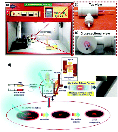
The co-axial electrospinning of aligned CF@PtNP based nanosystems was performed by dispersing PAN (10% w/v) in DMF and stirring for 5 h and for the shell material, 2 mg mL−1 10 mM H2PtCl6 was dispersed in 8 wt% PVP in DMF and stirred for 5 h. Co-axial electrospinning was carried out using a built-in electrospinning set-up with UV-photoreduction. Two 10 mL syringes were integrated with a co-axial spinneret and attached to the feed pump. In order to control the movement of the feed solution, a syringe pump (Holmarc, Cochin) with a high voltage power supply (DC-Glassman High Voltage Inc., Model No: EH30P3, New Jersey, USA) with an output voltage range of 1–30 kV was used for co-axial electrospinning. The nozzle was connected to the positive terminal of the transformer and the negative terminal was connected to the collector. The procedure was optimized by analysing numerous associations of electrospinning parameters, like concentration of the polymer solution, distance between the nozzle and collector, voltage applied, flow rate, different gauges for core and shell solutions and the diameter of the needle in order to attain even nanofibers. All experiments were accomplished under ambient conditions (RH = 60%, temperature: 29 °C). A voltage of 25 kV was used for this study for precursor loaded PVP@PAN solutions with a distance of 21 cm from the needle to the collector. The flow rate used was 1 mL h−1 using a 22G needle for the core and an 18G needle for the shell material. During the co-axial electrospinning process, the spinning unit was exposed to UV radiation (λ = 254 nm) for photoreduction of the outer Pt2+/PVP solution to form metallic Pt nanoparticles, hence to develop heterojunctions on the core fibers. The fiber was directly deposited on the IDA electrode (collector) for 10 min to produce a few layers of nanofibers.These PAN fibers were converted into co-axial CF@PtNP based nanosystems via a two-step thermal method comprising stabilization and carbonization.20 The stabilization and carbonization of PAN fibers were executed in a tubular furnace containing a quartz tube. The nanofibers undergo heat treatment in air and under a N2 atmosphere in the furnace at controlled temperature with a rate of 2 °C min−1 and 3 °C min−1 retained for 1 h. For single-step fabrication of aligned CF@PtNP based nanosystems using coaxial electrospinning, the nanofibers were directly collected on the Au sputtered IDA so as to form aligned nanofibers. Similarly, aligned CF@AuNP–PtNP and CF@NiNP–PtNP based nanosystems were also fabricated directly on the Au sputtered IDA by adding chloroauric acid and nickel chloride along with hexachloroplatinic acid and PVP solution respectively to form the shell layers.
3. Results and discussion
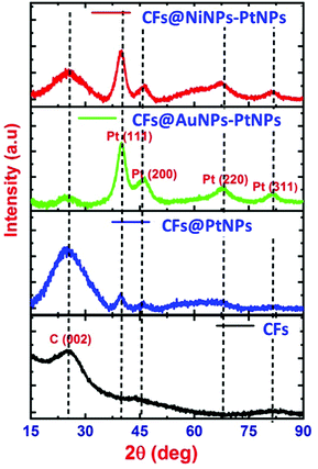
1D aligned core–shell CF@PtNP based nanosystems were fabricated using single step co-axial electrospinning with in situ photo reduction using polyacrylonitrile (PAN) solution as the core material and metals/bimetals (PtNPs, AuNPs–PtNPs and NiNPs–PtNPs) with polyvinyl pyrrolidone (PVP) solution as the shell material followed by stabilization (300 °C) and carbonization (950 °C) as depicted in Fig. 1. Monometallic and bimetallic (Au–Pt or Ni–Pt) nanoparticles in the shell layers were formed as a result of in situ UV irradiation (8 W) with a 254 nm UV source during co-axial electrospinning. The UV source is made to illuminate between positive (needle) and negative (copper sheet-collector) terminals of the electrospinning, which helps to reduce Pt2+ to Pt0 without any accumulation of Pt nanoclusters in the shell layer during thermal decomposition of polymers. Similarly, bimetallic nanoparticles (Au–Pt/Ni–Pt) were also formed during in situ UV irradiation. The formation of aligned nanofibers on the collector is depicted in Fig. 1. The jet would stretch itself across the gap as the field lines are attracted towards the electrodes. This induces the electrospun fibers to align themselves across the Au IDA electrode without any additional secondary voltage. Owing to the occurrence of charges on the fibers, mutual repulsion among the deposited fibers will increase the parallel and fairly even distribution of the fibers. This method may well be repetitive and a collection of monoaxial aligned fibers might be assembled on the big surface. Through this process, fibers with lengths in centimeters and diameters in the range of nanometers to micrometers can be developed in an aligned array. Thus, this fabrication method has several unique advantages over the prevailing methods for the fabrication of sensors. This method involves on-chip assembly of the materials onto detector substrates by means of economical co-axial electrospinning. Also, it proposes a one-stage process for the development of aligned heterojunction nanofibers with impressive control across the alignment of 1D fibers. In addition, this fabrication process eradicates solvent and impurity effects that happened during the synthesis of sensing materials via a chemical route, thereby improving the sensing properties. The co-axial fabrication allows for suitable monometallic and bimetallic functionalization of carbon nanofibers which improves the selectivity of the sensors. Thus, it offers a typical way for the complete insight into the interactions between analyte gas and sensor materials so as to elucidate the complicated sensing mechanism.Fig. 2 shows the X-ray diffraction pattern of pristine CFs, co-axial CFs@PtNPs, co-axial CFs@AuNPs–PtNPs and CFs@NiNPs–PtNPs. A wide peak centered at 25.2° appeared for CFs, co-axial CFs@PtNPs, CFs@AuNPs–PtNPs and CFs@NiNPs–PtNPs, which is attributed to the amorphous phase of the graphitic carbon ((002) plane) prevailing in the CFs (JCPDS card 41-1487).21,23 The XRD pattern of co-axial CFs@PtNPs confirms the existence of the characteristic peaks located at 2θ = 39.7°, 45.4°, 67.9° and 81.2°, which were ascribed to the planes (111), (200), (220) and (311) consistent with the fcc platinum (JCPDS card 04-0802), respectively.24 The average particle size (dhkl) of Pt was estimated using the Debye Scherrer equation to be 2.4 nm. The d-spacing of the co-axial CF@PtNP nanosystem was found to be 0.226 nm which is related to the Pt(111) plane with a lattice parameter a = 0.392 nm and is comparable with previous reports. Furthermore, platinum oxide peaks have not appeared in the XRD patterns depicted in Fig. 2.
The XRD pattern of the co-axial CF@AuNP–PtNP based nanosystem exhibited peaks at 2θ values of 40.02°, 46.2°, 68.4° and 81.9° corresponding to (111), (200), (220) and (311) planes of fcc crystal structure of Pt respectively (JCPDS card 04-0802). The inter d-spacing of co-axial CFs@AuNPs–PtNPs was found to be 0.2254 nm which is related to the Pt(111) plane with a lattice parameter a = 0.3904 nm. Overlapped peaks of Au and Pt further indicate that the nanoparticles are bimetallic in nature.25,26 Similarly, the XRD pattern of co-axial CFs@NiNPs–PtNPs displayed both strong and sharp peaks at 40.25°, 46.6°, 67.4°and 81.9° corresponding to (111), (200), (220) and (311) planes of fcc crystal structure of Pt respectively (JCPDS card 04-0802). The d-spacing of the co-axial CF@Ni NP–Pt NP based nanosystem was found to be 0.2251 nm which is related to the Pt(111) plane with a lattice parameter a = 0.389 nm. Overlap of the peaks of Ni and Pt further indicates that the nanoparticles are bimetallic in nature.21,27,28 A close observation of XRD patterns of co-axial bimetallic systems CFs@AuNPs–PtNPs and CFs@NiNPs–PtNPs reveals that the peak corresponding to the (111) plane of Pt has shifted to higher Bragg angles. From Fig. 2, it can also be confirmed that there is no any peak matching fcc Ni or NiO for co-axial CFs@NiNPs–PtNPs. The shift towards higher Bragg angles associated with pristine Pt might be owing to the constricting strain induced by the formation of bimetallic Pt with Au and Pt with Ni on CFs during the formation of co-axial bimetallic systems, CFs@AuNPs–PtNPs and CFs@NiNPs–PtNPs, which can effectively modify the adsorption energy of metal catalysts, and sequentially refine the catalytic activity.29
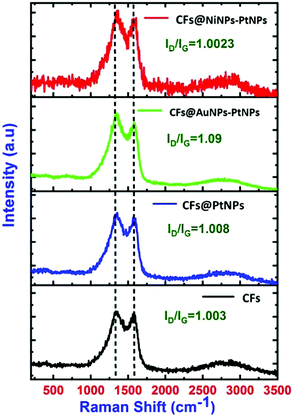
Raman spectral analysis was executed to understand the chemical identification of pristine CFs and co-axial CFs@PtNPs, CFs@AuNPs–PtNPs and CFs@NiNPs–PtNPs (Fig. 3). For pristine CFs, two characteristic peaks, i.e., D and G bands were spotted at 1335.7 cm−1 and 1580 cm−1, which are ascribed to the structural distortions triggered via the defects existing in the sp2 carbon network and E2g phonon mode of sp2 carbon atoms. A red shift was noticed for the D band (1354.6 cm−1) and G band (1568.4 cm−1) in co-axial CFs@PtNPs and the ID/IG ratio was amplified (1.008) compared to bare CFs (1.003), which can be attributed to the structural alterations owing to the interaction of platinum nanoparticles with the CF support. Similarly, for co-axial CFs@AuNPs–PtNPs, the D and G bands were found to be at 1360 cm−1 and 1587 cm−1 and for co-axial CFs@NiNPs–PtNPs, the D and G bands were found to be at 1367 cm−1 and 1606.6 cm−1 respectively. The ID/IG ratio for co-axial CFs@AuNPs–PtNPs was 1.09 and for co-axial CFs@NiNPs–PtNPs, it was estimated to be 1.0023. The higher intensity of the ID/IG peak for co-axial CFs@AuNPs–PtNPs may be due to the SERS enhancement upon introduction of plasmonic Au in the CF based bimetallic nanosystem.20,30
The structural and morphological analysis of the co-axial electrospun CF based bimetallic nanosystem was further executed by scanning electron microscopy (SEM) and transmission electron microscopy (TEM) analysis. The electric-field lines in the gap between Cu electrodes are drawn towards the electrode edges as seen in the electric field profile in Fig. 4a. Fig. 4b shows the SEM image of directly fabricated aligned co-axial CFs@NiNPs–PtNPs on the IDA before heat treatment. The as spun fibers have the length in micrometers, which aids in continuous charge transport in chemiresistive based gas sensors. Here, the alignment of nanofibers can be explained by “gap electrospinning”.31,32 The as-spun nanofibers are taken as a string of positively charged elements associated through a viscoelastic medium. This may result in experiencing two sets of electrostatic forces by the charged nanofibers: (i) ‘Fa’ acting between the charged fiber and charges brought on the two parallel grounded electrodes and (ii) ‘Fb’ formed by the splitting of the electric field. As per Coulomb's law of interaction, the fibers adjacent to the electrodes produce the sturdiest electrostatic force (Fa), which results in the elongation of nanofibers across the collector (parallel copper sheets) to produce aligned co-axial nanofibers.
 | ||
| Fig. 4 (a) Schematic illustration of gap electrospinning to generate aligned fibers and (b) SEM image of co-axially aligned fibers. | ||
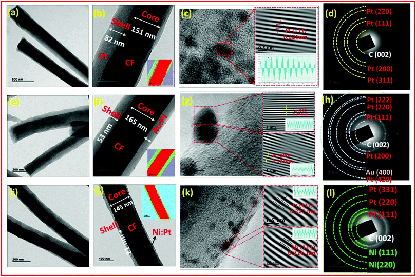
The co-axial morphology and distribution of the metallic/bimetallic nanoparticles over the fibers was confirmed using TEM as shown in Fig. 5. The lower magnification images displayed uniform arrangement of PtNPs, AuNPs–PtNPs and NiNPs–PtNPs formed on CFs with a mean diameter of 4.49, 4.13 and 2.73 nm. The core–shell structure of the co-axial CFs@PtNPs, CFs@AuNPs–PtNPs and CFs@NiNPs–PtNPs was evident from TEM images as depicted in Fig. 5(a and b). Fast Fourier transform (FFT) was employed by masking to eradicate undesirable noise and hence to disclose the anticipated frequencies by means of Gatan Microscopy Suite software. In order to get the real image on the masked region in the FFT pattern, an inverse Fourier transform (IFFT) was employed. The IFFT of the HRTEM images of co-axial CFs@PtNPs (Fig. 5c) revealed a lattice d-spacing of 0.226 nm corresponding to the (111) crystalline plane of fcc Pt anchored on CFs.33
From Fig. 5(e), it can be understood that in the case of co-axial CFs@AuNPs–PtNPs, the bimetallic AuNPs–PtNPs were homogenously distributed on CFs with a mean diameter of 4.13 nm. The HRTEM and FFT study of the core–shell CF@AuNP-PtNP nanosystem were further performed. IFFT analysis of co-axial CFs@AuNPs–PtNPs (Fig. 5g) exhibited a lattice spacing of 0.194 nm and 0.204 nm, conforming to the d-spacing values of Pt(200) and Au(200) planes.34–36 These results show that AuNPs and PtNPs occur as bimetallic NPs in the co-axial CF@AuNP-PtNP nanosystem. The selected area diffraction (SAED) pattern shown in Fig. 5h displayed spot patterns allocated to (111), (200), (220), (222) and (420) planes of fcc Pt crystals and the spot patterns allocated to the (400) plane of fcc Au, showing the polycrystalline nature of Au and Pt, which was in good agreement with the inferences attained by XRD patterns of the bimetallic Au–Pt nanosystem showing the development of bimetallic AuNPs–PtNPs on CFs.20
Similarly, as shown in Fig. 5i, co-axial CFs@NiNPs–PtNPs were also found to be successfully formed and were consistently dispersed on CFs with an average diameter of 2.9 nm. The HRTEM and FFT images of the core–shell CF@NiNP–PtNP based nanosystem were recorded for further structural elucidation. IFFT analysis of co-axial CFs@NiNPs–PtNPs (Fig. 5k) showed lattice spacings of 0.227 nm and 0.216 nm, conforming to the d values of Pt(111) and Ni(111) planes respectively.37 These observations specify that Ni and Pt nanoparticles occur as bimetallic nanoparticles in the co-axial CFs@NiNPs–PtNPs produced through the single-step coaxial Fig. 5l displays spot patterns ascribed to (111), (220) and (331) planes of fcc Pt crystals and spot patterns allocated to (111) and (220) planes of fcc Ni crystals discussed the electrospinning method. SAED pattern analysis showed polycrystalline nature of Ni and Pt, showing a decent agreement with the inferences attained from XRD analysis of co-axial CFs@NiNPs–PtNPs, verifying the bimetallic formation of NiNP–PtNP nanostructures on CFs. From the morphological investigations, it is obvious that co-axial bimetallic NiNPs–PtNPs on CFs showed reduced sizes of nanoparticles and homogeneous distribution over CFs, which can proficiently enable the “spillover effect” during adsorption of H2 compared to other co-axial CF@PtNP based nanosystems and can result in better sensor performance.
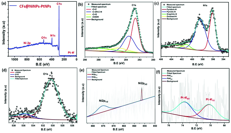
In order to understand the surface chemical states of co-axial CF@PtNP based nanosystems, XPS analysis was carried out. High-resolution spectra of co-axial CFs@NiNPs–PtNPs consisted of oxygen 1s (O 1s), carbon 1s (C 1s), nitrogen 1s (N 1s), nickel 2p (Ni 2p) and platinum 4f (Pt 4f) as depicted in Fig. 6. The survey scan spectra of co-axial CFs@NiNPs–PtNPs illustrated in Fig. 6a exhibit five prominent peaks at 530.3, 396, 283, 875.2 and 73 eV conforming to O 1s, C 1s, N 1s, Ni 2p and Pt 4f, which confirmed the existence of elements, such as oxygen, carbon, nitrogen, nickel and platinum. The C 1s peak (Fig. 6b) can be deconvoluted into four peaks, attributed to the C![[double bond, length as m-dash]](https://www.rsc.org/images/entities/char_e001.gif) C bond (282.6 eV), C–OH bond and C–N bond (283.6 eV), C
C bond (282.6 eV), C–OH bond and C–N bond (283.6 eV), C![[double bond, length as m-dash]](https://www.rsc.org/images/entities/char_e001.gif) O bond (285.2 eV) and –COOH (287.4 eV), respectively. The C
O bond (285.2 eV) and –COOH (287.4 eV), respectively. The C![[double bond, length as m-dash]](https://www.rsc.org/images/entities/char_e001.gif) C bond (282.6 eV) originated from the amorphous carbon. The peaks at 283.6 eV and 285.2 eV are the distinctive characteristics of C–OH groups and C
C bond (282.6 eV) originated from the amorphous carbon. The peaks at 283.6 eV and 285.2 eV are the distinctive characteristics of C–OH groups and C![[double bond, length as m-dash]](https://www.rsc.org/images/entities/char_e001.gif) O bonds. The high-resolution O 1s spectra of co-axial CFs@NiNPs–PtNPs (Fig. 6d) show the presence of C
O bonds. The high-resolution O 1s spectra of co-axial CFs@NiNPs–PtNPs (Fig. 6d) show the presence of C![[double bond, length as m-dash]](https://www.rsc.org/images/entities/char_e001.gif) O (530.32 eV), and oxygen vacancies (535.7 eV).38 The N 1s spectra (Fig. 6c) can be deconvoluted into three peaks at 396.13, 398.5, 401.2 and 403.2 eV attributed to the pyridinic nitrogen, pyrrolic nitrogen, graphitic nitrogen and pyridinic–N-oxide respectively. Amongst these groups the pyridinic and pyrrolic nitrogen aids in lessening of charge transport resistance and thereby can boost up the catalytic effects due to the sp2 hybridized nitrogen atom.39 The Pt 4f exhibited two peaks emerging at 70.2 and 73.7 eV, which originate from the spin orbital coupling of 4f photoelectron transitions as observed from Fig. 6f. The lowermost B.E. components linked might be ascribed to the zero valent state of metallic platinum NPs.20,21
O (530.32 eV), and oxygen vacancies (535.7 eV).38 The N 1s spectra (Fig. 6c) can be deconvoluted into three peaks at 396.13, 398.5, 401.2 and 403.2 eV attributed to the pyridinic nitrogen, pyrrolic nitrogen, graphitic nitrogen and pyridinic–N-oxide respectively. Amongst these groups the pyridinic and pyrrolic nitrogen aids in lessening of charge transport resistance and thereby can boost up the catalytic effects due to the sp2 hybridized nitrogen atom.39 The Pt 4f exhibited two peaks emerging at 70.2 and 73.7 eV, which originate from the spin orbital coupling of 4f photoelectron transitions as observed from Fig. 6f. The lowermost B.E. components linked might be ascribed to the zero valent state of metallic platinum NPs.20,21
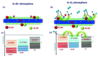
The Ni 2p spectrum40,41 unveiled two weak peaks emerging at 875.2 and 856.41 eV, ascribed to the binding energies of Ni 2p1/2 and Ni 2p3/2 as shown in Fig. 6e. Besides, from the XPS spectra it was confirmed that there were no any further impurity peaks, and the major Pt 4f and Ni 2p peaks confirmed the emergence of NiNPs–PtNPs bimetallic NPs on CFs by the single-step co-axial electrospinning method. In addition, Fig. 7 compares the Pt 4f spectra of co-axial CFs@PtNPs, co-axial CFs@AuNPs–PtNPs and co-axial CFs@NiNPs–PtNPs. The charge transfer occurring in co-axial CFs@NiNPs–PtNPs is apparent in XPS (Fig. 7) spectra. The high resolution XPS spectra of CFs@PtNPs and co-axial CFs@AuNPs–PtNPs are depicted in Fig. S1 and S2 (ESI†). In the case of co-axial CFs@AuNPs–PtNPs, the binding energy of Pt 4f spectra was shifted slightly to higher energy, which directs towards the solid interaction prevailing among metallic Au, Pt and the CFs. The B. E. shift can pave the way for electron density shift from the bimetallic AuNPs–PtNPs to the CFs. Thereby, the work function lowered for CFs@AuNPs–PtNPs. Therefore, to equilibrate the Fermi levels, transfer of charge carriers from PtNPs to AuNPs and then to CFs occurs.20
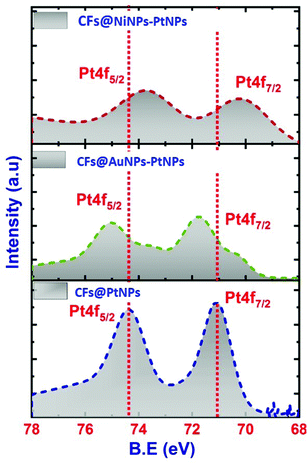 | ||
| Fig. 7 High resolution XPS spectra corresponding to Pt 4f of co-axial CF@PtNP, CF@AuNP-PtNP and CF@NiNP–PtNP based nanosystems. | ||
Hence, XPS analysis significantly supports the emergence of bimetallic AuNPs–PtNPs on CFs. In contrast, for co-axial CFs@NiNPs–PtNPs, the binding energy of the Pt 4f peak was shifted slightly to lower energy (Fig. 7), signifying a sturdy interaction prevailing among metallic Ni, Pt and the CFs. This shift may be caused by the transfer of electrons from Ni to Pt owing to the difference in electronegative values of Ni (1.91) and Pt (2.28), which results in a variation in the electronic properties of Pt, i.e., lowering the density of states on the Fermi level in co-axial CFs@NiNPs–PtNPs. Hence, the bimetallic formation with Ni altered the electronic properties of Pt, resulting in an improvement of catalytic performance.42,43 Besides, in bimetallic Pt based co-axial CF nanosystems, the Pt 4f peak gets widened. This possibly would be because of the overlapping of the Ni 3p peak with the Pt 4f7/2 peak. These results also substantiate the observations from XRD and HRTEM analysis.
3.1 Hydrogen gas sensor performance evaluation of 1D aligned co-axial CF@PtNP based nanosystems
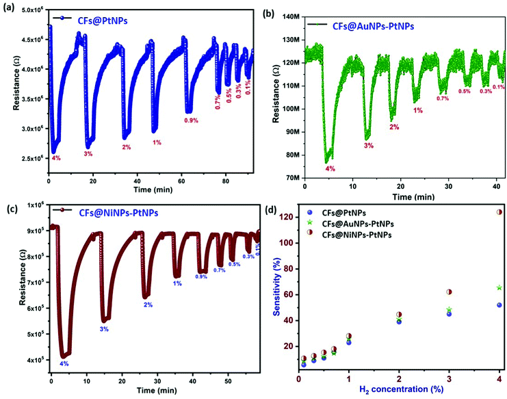
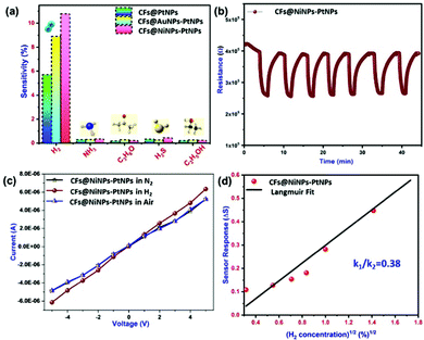
Hydrogen gas sensing studies of on-chip fabricated electrospun 1D aligned co-axial CFs@PtNPs, CFs@AuNPs–PtNPs and CFs@NiNPs–PtNPs were performed at room temperature by means of a built-in sensor test station. Initially, the sensor resistance was stabilized by purging N2 into the chamber to eliminate the impurities. Upon exposure to H2 gas, the resistance of the 1D aligned co-axial CFs@NiNPs–PtNPs was decreased drastically, in agreement with earlier reports. Fig. 8a–c depicts the dynamic gas sensing response of aligned co-axial CFs@PtNPs, aligned co-axial CFs@AuNPs–PtNPs and aligned co-axial CFs@NiNPs–PtNPs towards hydrogen in the range of 0.1% to 4%. Fig. 8a illustrates the dynamic gas sensing response of 1D aligned co-axial CFs@PtNPs, which depicts the sensitivity extending from 5.7% to 52% towards exposure to 0.1% to 4% of H2 gas at RT. The sensor response of 1D aligned co-axial CFs@PtNPs towards hydrogen is attributable to the excellent adsorption property of hydrogen on the platinum surface. During the recovery process of the sensor, the chemisorbed H2 was desorbed back from the surface by air. However, the co-axial CF@PtNP sensor took extra time to recover to the baseline resistance as a result of the emergence of platinum hydride amongst nanohybrids. Fig. 8b describes the dynamic response of co-axial CFs@AuNPs–PtNPs towards H2 concentrations ranging from 0.1% to 4% which exhibited sensitivity in the range of 8.9% to 62% at room temperature. During sensor recovery, the resistance of 1D aligned co-axial CFs@AuNPs–PtNPs regained the base resistance more swiftly than co-axial CFs@PtNPs. This might be due to the integration of bimetallic AuNP-PtNP catalysts over the core CFs. The surface anchored bimetallic AuNPs–PtNPs also reduce the emergence of platinum hydride and thereby, increase the catalytic sites produced on the CFs towards H2 gas which resulted in the improved sensor response and recovery time.Fig. 8c demonstrates the dynamic sensor response of 1D aligned co-axial CFs@NiNPs–PtNPs towards H2 gas with a concentration ranging from 0.1% to 4% at room temperature which exhibited sensitivity in the range of 10.8% to 124% with a sensor response time and recovery of 24 s and 89 s (towards 4% of H2). Thus, the 1D aligned co-axial CF@NiNP–PtNP sensor exhibited superior adsorption towards H2 which may be due to the bimetallic NiNP–PtNP catalytic active sites present over the core CFs. The sensor performances of co-axial CFs@PtNPs, CFs@AuNPs–PtNPs and CFs@NiNPs–PtNPs are compared in Fig. 8d and tabulated in Table S1 (ESI†). The cross-interference of the H2 sensor towards different gases is a vital parameter for real-time application of the sensors (Fig. 9a). The sensor response towards interfering gases such as acetone, ammonia, ethanol and hydrogen sulphide (H2S) was tested to check the selectivity of 1D aligned co-axial CFs@PtNPs, CFs@AuNPs–PtNPs and CFs@NiNPs–PtNPs. Fig. 9b depicts the repeatability of the 1D aligned co-axial CF@NiNP–PtNP based sensor towards periodic exposure to 0.5% of H2 at room temperature.
Also, Figure S3 (ESI†) depicts the interference of humidity in the H2 sensing properties of CFs@NiNPs–PtNPs. It was observed that, with the increase in humidity, the H2 sensor response of CFs@NiNPs–PtNPs decreased. It might be due to the adsorption of water molecules on the sensor material, which prevents subsequent adsorption of H2 molecules, leading to a decrease in sensor performance. In situ current–voltage (I–V) studies performed for the 1D aligned co-axial CF@NiNP–PtNP sensor are depicted in Fig. 9c, performed before and after adsorption of hydrogen on the sensor, which revealed the considerable refinement of electron transport upon exposure to H2. In addition, the 1D aligned co-axial CF@NiNP–PtNP sensor showed similar responses without any remarkable shift in baseline resistance, upon exposure to 0.5% H2. 1D aligned co-axial CF@NiNP–PtNP sensor performance is compared with that of recently developed carbon based or metallic based sensors in Table 1. From the recent literature,44–46 it was clear that most of the reported H2 sensors were based on multi-step processes or complex processes or expensive methods or not suitable for real-time applications, whereas the aligned co-axial CF@NiNP–PtNP sensor was developed through a one-step fabrication of the sensor material, which can be easily upscaled for mass production for real-time applications. Also, the co-axial CF@NiNP–PtNP sensor showed rapid and stable ON/OFF cycles respectively. Along with the complicated fabrication processes adopted by previous reports, the non-linearity of the sensor responses at higher concentration was an another issue faced by H2 gas sensors.47 The aligned co-axial CF@NiNP–PtNP nanosystem not only achieved the ease in fabrication method, but also resolved the problem of non-linearity of H2 gas sensors at higher concentration of H2 at room temperature. This could be mainly due to the following reasons: (i) the bimetallic catalyst arrangement over the CFs, such that it “spill over”48,49 the adsorbed hydrogen on the surface of CFs and (ii) the direct single step fabrication of co-axial bimetallic aligned CF@NiNP–PtNP nanosystem, which eradicates the barrier formation for electron transport, usually occurring during the process of functionalization of carbon supports for metal attachment during wet chemical routes, which is not required in the case of direct co-axial fabrication processes.
| Sensor material | Fabrication method | Operating temp. (°C) | H2 conc. (ppm) | Sensitivity (%) |
|---|---|---|---|---|
| Graphene-supported Pt/Pd core–shells hybrid51 | Wet chemical route and air brush spraying | RT | 10![[thin space (1/6-em)]](https://www.rsc.org/images/entities/char_2009.gif) 000 000 |
36 |
| Pt-CNT48 | Spin coating and electron beam deposition | RT | 23![[thin space (1/6-em)]](https://www.rsc.org/images/entities/char_2009.gif) 000 000 |
16 |
| Pd thin films52 | RF sputtering | RT | 20![[thin space (1/6-em)]](https://www.rsc.org/images/entities/char_2009.gif) 000 000 |
12 |
| Pd Nanofilms53 | DC sputtering | RT | 1000 | 5.5 |
| Pt/Pd bimetallic thin film54 | PLD | 150 | 10![[thin space (1/6-em)]](https://www.rsc.org/images/entities/char_2009.gif) 000 000 |
13.6 |
| (Pt/SiC) Nanoballs55 | DC/RF sputtering | 330 | 100 | 44 |
| Pt–PPy56 | LBL | RT | 1000 | 11.6 |
| Pd–MWCNTs57 | Electrodeposition | RT | 3![[thin space (1/6-em)]](https://www.rsc.org/images/entities/char_2009.gif) 00 00![[thin space (1/6-em)]](https://www.rsc.org/images/entities/char_2009.gif) 000 000 |
16 |
| Palladium–organic Fibers58 | Sputtering (DC) | RT | 25 | 12.2 |
| Pd/GO/PAH/PSS/PAH59 | Layer by layer | RT | 1000 | 2.04 |
| CFs/ZnO60 | Electrospinning and RF sputtering | 150 | 100 | 73.4 |
| Co-axially aligned CFs@NiNPs–PtNPs nanosystemThis work | Co-axial electrospinning (direct fabrication) | RT | 1000 | 10.8 |
40![[thin space (1/6-em)]](https://www.rsc.org/images/entities/char_2009.gif) 000 000 |
124 |
The linear relation between response and the square root of H2 gas was confirmed by Langmuir isotherm theory50 of dissociative adsorption of gases on metal surfaces. Based on this theory, adsorption and desorption rates are described as k1[H2](1 − θ)2and k2θ2, where [H2] is the hydrogen concentration, θ is the surface coverage, and adsorption and desorption rate constants are denoted by k1 and k2. Upon steadiness, the rate of hydrogen surface coverage becomes negligible and thus adsorption rate is equivalent to desorption rate, i.e., k1[H2](1 − θ)2 = k2θ2. Hence, gas sensor response is relative to surface coverage (θ), by eqn (1)
 | (1) |
In the case of the co-axial CF@PtNP based nanosystem, H2 molecules detach and adsorb on the catalytic sites of CF@PtNP based systems (PtNPs, AuNPs–PtNPs and NiNPs–PtNPs) as given by eqn (2).
 | (2) |
During the sensor recovery, existence of oxygen in the air enabled the water formation with adsorbed H2 at the NiNP–PtNP surface. The nature of sensor recovery stipulates that the surface chemistry is a vital factor in the execution of successful chemi-resistive sensors. Even though aligned co-axial bimetallic AuNPs–PtNPs on CFs possess rapid recovery of the sensor at room temperature with long-term stability, the sensitivity of the sensor was found to be less, whereas aligned co-axial bimetallic NiNPs–PtNPs over CFs showed improved sensitivity with good sensor response time and recovery, making it an ideal H2 sensor material. This is due to the high catalytic activity of the NiNP–PtNP bimetallic system towards hydrogen. Generally, elements of group 10 in the periodic table, like Ni, Pt, and Pd, and their alloys are recognised for their high catalytic activity towards hydrogen. Their slightly filled “d” orbitals play a prominent role in the catalytic activity. Previous reports show that hydrogen molecules get initially chemisorbed on such metals and detach into highly reactive hydrogen, that eventually spills over to the near surfaces.62
Therefore, the less-Pt bimetallic NiNP–PtNP nanocatalyst functionalized CFs, which showed a synergistic effect of both metals with improved catalytic activity, is potentially suitable as a H2 sensing material at room temperature. Henceforth, the prototype of the H2 sensor based on 1D aligned co-axial CFs@NiNPs–PtNPs was demonstrated for the development of read-out electronic circuits. Thus, for real-time applications, single-step fabrication of 1D aligned co-axial CFs@bimetallic NiNPs–PtNPs on the sensor device is a convenient and cost-effective method towards H2 gas sensor development.
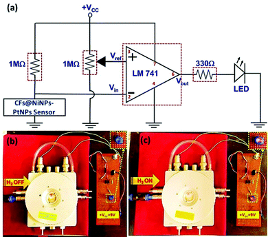
A prototype device based on the aligned co-axial CF@NiNP–PtNP sensor was further fabricated based on the equivalent electronic circuit diagram depicted in Fig. 11. The connections were made on a prototype universal printed circuit board (PCB). Real time detection of H2 gas was performed with the aligned co-axial CF@NiNP–PtNP sensor with the fabricated electronic circuit configuration. An LM741 operational amplifier IC was used, which works as a comparator circuit. A power supply of 9 V was given from the battery to the op-amp. The comparator compares voltages/resistance at inputs and produces an output with the voltage/resistance comparison. Therefore, in this comparator circuit, a potentiometer (1 MΩ) was connected to the non-inverting input, which is the reference voltage/resistance (Vref). To the inverting input, the potential across a series resistance (1 MΩ) and output of the 1D aligned co-axial CF@NiNP–PtNP sensor was given, which forms Vin. Since, the input was given to the inverting configuration, it is called a negative voltage comparator. That is, when the input signal is more negative than the reference voltage (Vref), it results in a high output voltage, Vout. When H2 is in the OFF state, the sensor unit displayed constant resistance and therefore the LED will be in OFF condition. When the H2 is introduced to the sensor device, a change in resistance of the sensor occurs (resistance decreases), which varies the comparator input, resulting in glowing of the LED. Hence, the real time monitoring of H2 gas at room temperature authenticates that the proposed device can be used for achieving ideal sensor characteristics.
4. Conclusions
To summarize, a direct single-step fabrication strategy for the synthesis of 1D aligned electrospun co-axial CFs@PtNPs, co-axial CFs@AuNPs–PtNPs and co-axial CFs@NiNPs–PtNPs was demonstrated towards H2 gas sensing at RT. Broad detection of H2 (0.1% to 4%) using aligned co-axial CFs@NiNPs–PtNPs showed superior H2 gas sensing performance (124%) compared to CFs@PtNPs (52%) and CFs@AuNPs–PtNPs (65.4%) at room temperature which may be due to the superior catalytic property of both Ni and Pt. The hydrogen adsorption kinetics disclosed that the adsorbed hydrogen on the surface of bimetallic NPs modifies the work function of the aligned co-axial CF@NiNP–PtNP sensor, which subsequently modifies the resistance. The non-linearity in sensitivity of H2 gas sensors at higher concentration was however eliminated by implementing the directly fabricated core–shell structure of CFs@NiNPs–PtNPs. In addition, the aligned fabrication of core–shell nanofibers aids to abolish the obstruction during the electron transport throughout the sensor, which thereby resulted in enhanced sensor performance. The theoretical prediction of the adsorption rate constant was analogous to the experimental value attained for the aligned co-axial CF@NiNP–PtNP based nanosystem. The on-screen monitoring of H2 interaction with aligned co-axial CFs@NiNPs–PtNPs was studied using in situ current voltage characteristics, which provided the authentication of interaction of H2 with the sensor material. Furthermore, a prototype device was successfully fabricated using the 1D aligned co-axial CF@NiNP–PtNP based sensor towards H2 gas detection at room temperature, which opens up its relevance for real time monitoring applications.Author contributions
The manuscript was written through contributions from all authors. All authors have given approval to the final version of the manuscript.Funding sources
This work is funded by DST-SERB (Ref: SB/S3/CE/038/2015).Conflicts of interest
There are no conflicts to declare.Acknowledgements
The authors wish to acknowledge DST-SERB (Ref: SB/S3/CE/038/2015) for financial support. The authors also acknowledge the facilities and support provided by the management, PSG Sons and Charities, Coimbatore.References
- T. Hübert, L. Boon-Brett, G. Black and U. Banach, Sens. Actuators, B, 2011, 157, 329–352 CrossRef.
- H. Hashtroudi, P. Atkin, I. D. R. Mackinnon and M. Shafiei, Int. J. Hydrogen Energy, 2019, 44, 26646–26664 CrossRef CAS.
- G. Manjavacas and B. Nieto, Hydrogen sensors and detectors, Elsevier Ltd., 2016 Search PubMed.
- W. J. Buttner, M. B. Post, R. Burgess and C. Rivkin, Int. J. Hydrogen Energy, 2011, 36, 2462–2470 CrossRef CAS.
- Y. F. Sun, S. B. Liu, F. L. Meng, J. Y. Liu, Z. Jin, L. T. Kong and J. H. Liu, Sensors, 2012, 12, 2610–2631 CrossRef CAS PubMed.
- Z. Wang, S. Wu, J. Wang, A. Yu and G. Wei, Nanomaterials, 2019, 9(7), 1045 CrossRef CAS.
- N. Jaggi and S. Dhall, International Scholarly and Scientific Research & Innovation, 2014, vol. 8, pp. 1295–1298 Search PubMed.
- Y. Luo, C. Zhang, B. Zheng, X. Geng and M. Debliquy, Int. J. Hydrogen Energy, 2017, 42, 20386–20397 CrossRef CAS.
- X. Li and J. Wang, InfoMat, 2020, 2, 3–32 CrossRef CAS.
- X. Zhou, Y. Wang, C. Gong, B. Liu and G. Wei, Chem. Eng. J., 2020, 402, 126189 CrossRef CAS.
- X. Zhou, B. Liu, Y. Chen, L. Guo and G. Wei, Mater. Adv., 2020, 1, 2163–2181 RSC.
- J. C. Ruiz-Cornejo, D. Sebastián and M. J. Lázaro, Rev. Chem. Eng., 2020, 36, 493–511 CAS.
- A. G. El-Deen, N. A. M. Barakat, K. A. Khalil and H. Y. Kim, New J. Chem., 2014, 38, 198–205 RSC.
- R. Vishnuraj, J. Dhakshinamoorthy, K. G. Nair, M. Aleem and B. Pullithadathil, Mater. Adv., 2021, 2, 3000 RSC.
- M. Eslamian, M. Khorrami, N. Yi, S. Majd and M. R. Abidian, J. Mater. Chem. B, 2019, 7, 224–232 RSC.
- S. Wu, B. Duan, P. Liu, C. Zhang, X. Qin and J. T. Butcher, ACS Appl. Mater. Interfaces, 2016, 8, 16950–16960 CrossRef CAS.
- R. Ferrando, J. Jellinek and R. L. Johnston, Chem. Rev., 2008, 108, 845–910 CrossRef CAS.
- Y. Peng, J. Ye and K. Zou, RSC Adv., 2016, 24880–24888 RSC.
- M. Baro and S. Ramaprabhu, Int. J. Hydrogen Energy, 2018, 1–9 Search PubMed.
- K. G. Nair, V. Ramakrishnan, R. Unnathpadi, K. K. Karuppanan and B. Pullithadathil, J. Phys. Chem. C, 2020, 124, 7144–7155 CrossRef CAS.
- K. G. Nair, R. Vishnuraj and B. Pullithadathil, ACS Appl. Electron. Mater., 2021, 3(4), 1621–1633 CrossRef CAS.
- J. Lei, Q. Zhang, Z. Zhao, Y. Chen, J. Gao, J. Tong, F. Peng and H. Xiao, Adv. Mater. Technol., 2020, 5, 1–9 Search PubMed.
- X. Mu, Z. Xu, Y. Ma, Y. Xie, H. Mi and J. Ma, Electrochim. Acta, 2017, 253, 171–177 CrossRef CAS.
- R. Sripada, V. Bhagavathi Parambath, M. Baro, S. P. Nagappan Nair and R. Sundara, Int. J. Hydrogen Energy, 2015, 40, 10346–10353 CrossRef CAS.
- J. Luo, M. M. Maye, V. Petkov, N. N. Kariuk, L. Wang, P. Njoki, D. Mott, Y. Lin and C. J. Zhong, Chem. Mater., 2005, 17, 3086–3091 CrossRef CAS.
- F. Fan, J. Zhang, J. Li, N. Zhang, R. R. Hong, X. Deng, P. Tang and D. Li, Sens. Actuators, B, 2017, 241, 895–903 CrossRef CAS.
- D. Song, S. Oh, H. Kim and E. Cho, Nano Lett., 2018, 18(4), 2450–2458 CrossRef PubMed.
- L. Ma, X. Wang, Q. Zhang, X. Tong, Y. Zhang and Z. Li, Anal. Methods, 2018, 10, 3845–3850 RSC.
- K. W. Park, J. H. Choi, B. K. Kwon, S. A. Lee, Y. E. Sung, H. Y. Ha, S. A. Hong, H. Kim and A. Wieckowski, J. Phys. Chem. B, 2002, 106, 1869–1877 CrossRef CAS.
- Y. Veera Manohara Reddy, B. Sravani, H. Maseed, T. Łuczak, M. Osińska, L. Subramanyamsarma, V. V. S. S. Srikanth and G. Madhavi, New J. Chem., 2018, 42, 16891–16901 RSC.
- D. Li, Y. Wang and Y. Xia, Nano Lett., 2003, 3, 1167–1171 CrossRef CAS.
- T. Lei, Z. Xu, X. Cai, L. Xu and D. Sun, Langmuir, 2018, 34, 13788–13793 CrossRef CAS PubMed.
- Z. Tian, C. Liu, Q. Li, J. Hou, Y. Li and S. Ai, Appl. Catal., A, 2015, 506, 134–142 CrossRef CAS.
- P. R. Sajanlal and T. Pradeep, Langmuir, 2010, 26, 8901–8907 CrossRef CAS PubMed.
- D. Wang, X. Cui, Q. Xiao, Y. Hu, Z. Wang, Y. M. Yiu and T. K. Sham, AIP Adv., 2018, 8(6), 065210 CrossRef.
- T. Ma, F. Liang, R. Chen, S. Liu and H. Zhang, Nanomaterials, 2017, 7(12), 431 CrossRef.
- J. Zhang, C. Chen, W. Yan, F. Duan, B. Zhang, Z. Gao and Y. Qin, Catal. Sci. Technol., 2016, 6, 2112–2119 RSC.
- N. T. Khoa, D. Van Thuan, S. W. Kim, S. Park, T. Van Tam, W. M. Choi, S. Cho, E. J. Kim and S. H. Hahn, RSC Adv., 2016, 6, 1535–1541 RSC.
- K. K. Karuppanan, A. V. Raghu, M. K. Panthalingal, S. Ramanathan, T. Kumaresan and B. Pullithadathil, J. Mater. Chem. A, 2018, 6, 12768–12781 RSC.
- P. Wang, Q. Shao, J. Guo, L. Bu and X. Huang, Chem. Mater., 2020, 32, 3144–3149 CrossRef CAS.
- C. Cui, M. Ahmadi, F. Behafarid, L. Gan, M. Neumann, M. Heggen, B. R. Cuenya and P. Strasser, Faraday Discuss., 2013, 162, 91–112 RSC.
- P. K. Sahoo, B. Panigrahy and D. Bahadur, RSC Adv., 2014, 4, 48563–48571 RSC.
- F. Fan, J. Zhang, J. Li, N. Zhang, R. R. Hong, X. Deng, P. Tang and D. Li, Sens. Actuators, B, 2017, 241, 895–903 CrossRef CAS.
- H. Kim, J. Yun, M. Gao, H. Kim, M. Cho and I. Park, ACS Appl. Mater. Interfaces, 2020, 12, 43614–43623 CrossRef CAS.
- C. Lupan, R. Khaledialidusti, A. K. Mishra, V. Postica, M. I. Terasa, N. Magariu, T. Pauporté, B. Viana, J. Drewes, A. Vahl, F. Faupel and R. Adelung, ACS Appl. Mater. Interfaces, 2020, 12, 24951–24964 CrossRef CAS.
- S. Yadav, A. Nair, M. B. Kusuma Urs and V. B. Kamble, ACS Appl. Nano Mater., 2020, 3, 10082–10093 CrossRef CAS.
- R. D. Martínez-Orozco, R. Antaño-López and V. Rodríguez-González, New J. Chem., 2015, 39, 8044–8054 RSC.
- D. Jung, M. Han and G. S. Lee, ACS Appl. Mater. Interfaces, 2015, 7, 3050–3057 CrossRef CAS PubMed.
- H. J. Cho, V. T. Chen, S. Qiao, W. T. Koo, R. M. Penner and I. D. Kim, ACS Sens., 2018, 3, 2152–2158 CrossRef CAS PubMed.
- I. Lundström, S. Shivaraman, C. Svensson and L. Lundkvist, Appl. Phys. Lett., 1975, 26, 55–57 CrossRef.
- D. T. Phan, A. S. M. I. Uddin and G. S. Chung, Sens. Actuators, B, 2015, 220, 962–967 CrossRef CAS.
- S. Öztürk and N. Kılınç, J. Alloys Compd., 2016, 674, 179–184 CrossRef.
- B. Xie, P. Mao, M. Chen, Z. Li, J. Han, L. Yang, X. Wang, M. Han, J. M. Liu and G. Wang, ACS Appl. Mater. Interfaces, 2018, 10, 44603–44613 CrossRef CAS.
- K. Hassan, A. S. M. Iftekhar Uddin and G. S. Chung, Sens. Actuators, B, 2016, 234, 435–445 CrossRef CAS.
- N. Singh, A. Kumar and D. Kaur, Sens. Actuators, B, 2018, 262, 162–170 CrossRef CAS.
- P. G. Su and C. C. Shiu, Sens. Actuators, B, 2011, 157, 275–281 CrossRef CAS.
- M. Han, D. Jung and G. S. Lee, Chem. Phys. Lett., 2014, 610–611, 261–266 CrossRef CAS.
- H. Jiang, Y. Yu, L. Zhang, J. Zhu, X. Zhao and W. Zhang, Sensors, 2019, 19(6), 1290 CrossRef CAS PubMed.
- P. G. Su and S. Lin-Kuo, Anal. Methods, 2020, 12, 3537–3544 RSC.
- V. Singh Bhati, A. Nathani, A. Nigam, C. S. Sharma and M. Kumar, Sens. Actuators, B, 2019, 299, 126980 CrossRef CAS.
- Z. Wang, Z. Li, T. Jiang, X. Xu and C. Wang, ACS Appl. Mater. Interfaces, 2013, 5, 2013–2021 CrossRef CAS.
- T. M. David, K. I. Gnanasekar, P. Wilson, P. Sagayaraj and T. Mathews, ACS Omega, 2020, 5, 11352–11360 CrossRef CAS.
Footnote |
| † Electronic supplementary information (ESI) available: High resolution XPS spectrum of CFs@PtNPs and CFs@AuNPs-PtNPs. See DOI: 10.1039/d1ma00683e |
| This journal is © The Royal Society of Chemistry 2022 |

