
 Open Access Article
 This Open Access Article is licensed under a Creative Commons Attribution-Non Commercial 3.0 Unported Licence
Mechanical strain, thermal and pressure effects on the absorption edge of an organic charge-transfer polymer for flexible photovoltaics and sensors†
Paulina
Ratajczyk
 a,
Andrzej
Katrusiak
*a,
Krzysztof A.
Bogdanowicz
b,
Wojciech
Przybył
b,
Piotr
Krysiak
b,
Anna
Kwak
b and
Agnieszka
Iwan
*b
a,
Andrzej
Katrusiak
*a,
Krzysztof A.
Bogdanowicz
b,
Wojciech
Przybył
b,
Piotr
Krysiak
b,
Anna
Kwak
b and
Agnieszka
Iwan
*b
aFaculty of Chemistry, Adam Mickiewicz University, Uniwersytetu Poznańskiego 8, 61-614 Poznań, Poland. E-mail: katran@amu.edu.pl
bMilitary Institute of Engineer Technology, Obornicka 136, 50-961 Wroclaw, Poland. E-mail: iwan@witi.wroc.pl
First published on 14th February 2022
Abstract
Mechanical and thermal strains in organic photovoltaic layers deposited on poly(ethylene terephthalate) (PET) and glass substrates and the resulting effect on the bandgap energy have been determined for the organic charge-transfer polymer PTB7. Its strong bathochromic shift of the absorption spectra under pressure also depends on the layer preparation method. The effects of different solvents and PTB7 concentrations on agglomerate formation were also studied. A perfect linear dependence of the concentration vs. absorbance was observed up to 1.81 × 10⁻⁷ M for chlorobenzene or o-dichlorobenzene solution. The thermal image monitoring of the current response at an increasing potential showed a linear current-to-voltage tendency, indicating that the conductive behaviour of the polymer depends on the substrate used in PET/ITO/PTB7/Ag/ITO/PET and glass/ITO/PTB7/Ag/ITO/glass devices. The PTB7 layer on the PET/ITO substrate displays superior mechanical properties suitable for flexible photovoltaic panels exposed to strain and deformations.
Introduction
New photovoltaic (PV) materials are intensively sought for operation, efficiency, and performance improvement, as well as for improving the mechanical properties and resistance to damage. Such materials would enable wider applications of photovoltaic cells, a goal that is directly connected to environmental protection. While most of the currently available photovoltaic panels are based on silicon technologies as well as other covalent and ionic materials, organic compounds offer significant advantages, such as a low production cost, easy processing (e.g., the formation of thin layers through painting or spraying any-shaped surfaces), practically infinite means of chemical modifications aimed at improving the efficiency, durability, and good elastic performance for applications in flexible screens, panels and cloth.1 The organic polymer flexible panels are light, cheap to produce and easily disposed of.At present, organic/polymer solar cells are being widely investigated in a few main directions: (i) the application of new polymers, copolymers or small compounds in the active layer of PV devices,2–7 (ii) the application of graphene, graphene oxide, their chemical modifications, carbon nanotubes, fullerenes and nonfullerenes, and their derivatives either as an active layer or as an interlayer in PV devices,8–14 (iii) the application of new polymers or graphene as flexible substrates in PV devices15–17 and (iv) the application of new polymers as hole transporting layers (HTLs), instead of poly(3,4-ethylenedioxythiophene) polystyrene sulfonate (PEDOT:PSS), in PV devices.18,19
To construct the active layer in polymer photovoltaic devices, poly(3-hexylthiophene) (P3HT) and poly[N-9′′-heptadecanyl-2,7-carbazole-alt-5,5-(4′,7′-di-2-thienyl-2′,1′,3′-benzothiadiazole)] (PCDTBT) have been widely investigated as donor materials. Theoretical studies from 2008 predicted “realistically achievable” power conversion efficiency (PCE) values of ca. 15% for fully optimized donor–acceptor bulk heterojunction (BHJ) organic solar cells.20 The basic questions to be addressed centre on the relationships between the chemical and physical compositions of interlayer materials and their energetic and electrical properties on nanometre length scales, often in environments with the complexity of the working solar cell platform.
Most recently, various strategies have been used for optimizing the organic/polymeric solar cells, e.g.: (i) in order to manipulate the molecular interactions of the binary blend, environmentally friendly solvents were used as the third component of the active layer;21 (ii) efficient deposition techniques for perovskites and charge transport layers such as doctor-blade coating, slot-die coating, screen printing, and spray deposition strategies contributed to the significant development of large-area perovskite solar modules;22 (iii) small-molecule donor–acceptor mixtures were used as stable device architectures without intermediate electrode layers;23 (iv) a broad family of organoboron small molecular donors/acceptors and organoboron polymer donors/acceptors became an important class of organic photovoltaic materials;5 (v) the stability of organic solar cells was significantly increased via material design, device engineering of the active layers, employing an inverted geometry, optimizing the buffer layers, and using stable electrodes and encapsulation materials;7 (vi) several printing techniques improved the production of large-area flexible transparent conductive films (TCFs);24 (vii) novel nanomaterials were designed and developed, including carbon nanotubes, graphene and their composites, which are now the main materials for flexible and transparent thin-film electrodes;17,25,26 and (viii) radioactive sources were used to generate photonic light in scintillators as converters of ionizing radiation to electricity in photovoltaic cells.27
Poly[[4,8-bis[(2-ethylhexyl)oxy]benzo[1,2-b:4,5-b′]dithio-phene-2,6-diyl][3-fluoro-2-[(2-ethylhexyl)oxy]carbonyl]thieno [3,4-b]thiophenediyl] (PTB7) (Fig. 1) presently gives some of the highest reported efficiencies (PCE = 8.92%) for PTB7:PC71BM BHJ solar cells in the presence of 3.0 v% 1,8-diiodooctane (DIO) and 1 wt% polystyrene (PS).28 For the inverted architecture indium tin oxide (ITO)/poly[(9,9-bis(3′-(N,N-dimethylamino)propyl)-2,7-fluorene)-alt-2,7-(9,9-dioctylfluorene)] (PFN)/PTB7:PC71BM/MoO3/Al, the power conversion efficiency was found to be 9.15% (for standard BHJ solar cell ITO/PEDOT:PSS/PTB7:PC71BM/PFN/Ca, PCE = 8.24%).29 However, this efficiency is still far from the theoretical value of PCE, which is equal to 15%. One of the proposed ways to achieve or even exceed the theoretical value of PCE is the construction of tandem perovskite cells with ITO/SnO2/CsPbI2Br/P3HT/MoO3/Ag/PFN-Br/PTB7-Th:IEICO-4F/MoO3/Ag architectures containing poly([2,6′-4,8-di(5-ethylhexylthienyl)benzo[1,2-b;3,3-b]dithiophene]{3-fluoro-2[(2-ethylhexyl)carbonyl]thieno[3,4-b]thiophenediyl}) (PTB7-Th) as a component of the hole transporting material (HTM) layer with PCE = 17.24%.30
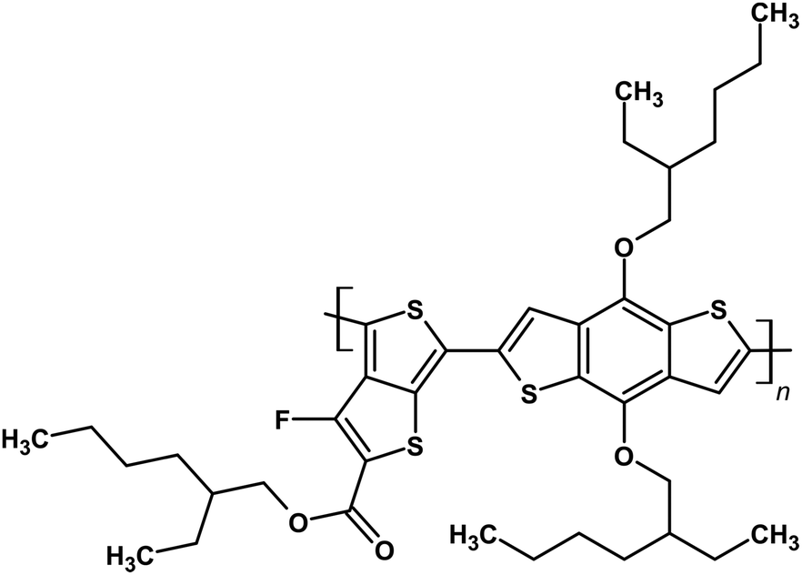 | ||
| Fig. 1 Molecular structure of PTB7. | ||
Murray et al. described the ITO/HTL/PTB7:PC71BM/LiF/Al architecture for polymer solar cells, where graphene oxide (GO) or PEDOT:PSS was used as the HTL.31 Devices with GO exhibited a PCE equal to 7.5%, indicating a 5-fold enhancement in the thermal aging lifetime and a 20-fold enhancement in the humid ambient lifetime versus analogous PEDOT:PSS-based devices.
It should be emphasized that polymer solar cells based only on PTB7 are utilized in the inverted device with the ITO/ZnO/PTB7/MoO3/Ag architecture, and the PCE value is only 0.14%, indicating almost no photovoltaic performance.32 For solar cells with an active layer based on PTB7:PC71BM or PTB7:PC71BM:DIO, the PCE values are 4.74% and 7.41%, respectively.
In addition to modifying the solar cell architecture, scientists are studying the selected electrochemical parameters of PTB7:PC71BM in detail to understand the differences in behaviour of this mixture compared to P3HT:PCBM. For example, Park et al. discovered that, at the PTB7:PC71BM interface, the interface dipole and band bending were not observed due to their identical charge neutrality levels. On the other hand, a large interfacial dipole was observed at the P3HT:PC61BM interface. It was found that the photovoltaic energy gaps (EPVG) were 1.10 eV and 0.90 eV for PTB7:PC71BM and P3HT:PC61BM, respectively, inducing a larger open-circuit voltage in PTB7:PC71BM than that in P3HT:PC61BM.33 Jin et al. investigated the transient THz conductivities of PTB7 and P3HT blended with PC71BM using ultrafast THz spectroscopy.34 They demonstrated that the carrier–carrier interactions at higher density play a significant role in decreasing the charge carrier mobility in PTB7:PC71BM. Transient absorption spectroscopy of PTB7:PC71BM blends containing a broad range of acceptor contents (0.01–50% by weight)35 showed that with the increase in the polaron signal PC71BM concentrations of more than 10%, most polarons are generated within 200 fs, while for lower acceptor concentrations, the polaron signal increases gradually over ∼1 ps, with most polarons generated after 200 fs.
Detailed studies on the selected properties of PTB7 led to new solutions for improving the charge mobility and morphology of PTB7. For example, Savikhin et al. studied the effect of high-temperature annealing on the properties of PTB7 and PTB7:fullerene blends and revealed that annealing at a moderate temperature (260 °C) improves the PTB7 morphology and optoelectronic properties.36 Although high-temperature annealing (290 °C) also improves the morphology, it caused poorer optoelectronic properties as an effect of aliphatic side chain modification in PTB7, increased electronic disorder and decreased mobility. It was found that solar irradiation modifies the chemical structure of PTB7 and affects the device photostability.
Kettle et al. studied the chemical degradation of PTB7 by X-ray photoelectron spectroscopy (XPS)37 and demonstrated that PTB7 seems to be essentially unstable when illuminated in air. XPS studies were used to confirm that the rapid photodegradation process occurs due to changes in the chemical structure of PTB7. The transient magnetic field effects of photoexcitation in PTB7 were studied by Huynh et al.38
Among the considerable number of techniques employed for studying solar cell properties in recent years, high-pressure techniques have been used to reveal the impressive potential of photovoltaics based on perovskites.39–46 Pressure is a fundamental thermodynamic variable that can induce a variety of structural changes, such as phase transitions,47 Jahn–Teller interplay with the lattice strain,48 and amorphization.49,50 Generally, high-pressure studies are ideal for understanding the structure–property relationship,51 as they provide fundamental insight into the structural, optoelectronic, and magnetic properties of materials and thus can guide the design of new photovoltaic materials with desired properties. An important feature of photovoltaic materials, generally used in the form of thin and thick layers, is the effect of strain on the absorption and current-generation efficiency. Strain can be generated in the layer-deposition process due to the layer–substrate interactions, as governed by the different multilayer thermal expansions in photovoltaic panels, the bending strain in flexible devices and other effects in the production process and specific applications in different environments. Furthermore, the operation of solar cells occurs with significant temperature changes that can amplify stress, which may completely alter the structure and optoelectronic properties of the materials, affecting their performance. Nowadays, strain engineering is increasingly used to tailor optoelectronic functionalities.52,53 To our knowledge, no pressure effects have been described for the absorption edge of organic photovoltaic materials. Therefore, we have undertaken this study on the photovoltaic polymer PTB7. Apart from the photovoltaic performance, we also continue to be interested in finding new materials for pressure sensors. Our present study includes the effects of solvents and additives on the morphological, optical, mechanical and electrical behaviours of the created PTB7 layer. We have shown that the PTB7-based panels endow flexible and adaptive multilayer systems offering sufficient performance of the bulk and interfaces for their operation under the strain required in flexible, wearable and exposed products under extreme conditions. Such a performance can result not only from high stretchability, but also from autonomous self-healing capabilities.
Results and discussion
The solubility of PTB7 was assessed through ultrasonication for 60 minutes with 1.0 mg of the sample and 1 mL of the solvent in a vial. Then, the vials were put aside for another 60 minutes, and the observations were noted. These tests showed good solubility in chlorinated solvents such as dichloroethane, dichloromethane and o-dichlorobenzene (o-DCB). Since PTB7 is a polymeric material, it requires more time to fully dissolve; hence, we left the compound overnight, and the ultrasonication was repeated.UV-vis in solution
First, a UV-vis study was performed for the solutions in chlorobenzene (CB) and o-DCB. The basic spectra in CB and o-DCB at a concentration of 6.62 × 10⁻³ mg mL−1 displayed a typical PTB7 shape with very similar absorption maxima for both solutions (Fig. 2). In the spectra, there are three main bands with maxima at 300, 621, and 680 nm.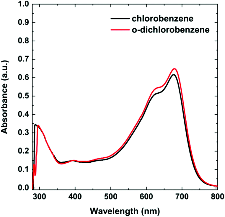 | ||
| Fig. 2 UV-vis spectra of PTB7 in chlorobenzene and o-dichlorobenzene. | ||
To establish the possible agglomerate formation depending on the type of solvent, we investigated a wide range of concentrations (Fig. 3), from 5.3 × 10⁻⁹ to 2.56 × 10⁻⁷ M (6.67 × 10⁻⁴ to 3.22 × 10⁻² mg mL−1), within the limit of 2.1 absorbance units. Following the changes in spectra, the ratios of the integrated intensities of the bands at 621 and 680 nm were compared. We found that the normalized signal for 680 nm reflected a change in the proportion from 1.21![[thin space (1/6-em)]](https://www.rsc.org/images/entities/char_2009.gif) :1/1.19:1 to nearly 1.10:1/1.06:1 for chlorobenzene/o-chlorobenzene. According to Zhang et al., this direction of change is due to the reduced polymer ordered aggregation in solution that occurs upon increasing the concentration.32 In our study, disordered aggregation was observed for concentrations above 1.81 × 10⁻⁷ M (2.28 × 10⁻² mg mL−1), which was evident for the solution in o-DCB. Thus, an almost perfect linear dependence of the concentration vs. absorbance was observed up to 1.81 × 10⁻⁷ M (2.28 × 10⁻² mg mL−1) for both solvents, with only a small discrepancy for the CB solution. This shows that the dipole-moment change from 1.54 D (CB) to 2.14 D (o-DCB) influences the in-solution aggregation ordering of the PTB7 polymer, resulting in a stronger disorder at higher concentrations. This relationship indicates that the dipole moment of solvent molecules has a similar effect on aggregation as the addition of DIO to the CB solution.32
:1/1.19:1 to nearly 1.10:1/1.06:1 for chlorobenzene/o-chlorobenzene. According to Zhang et al., this direction of change is due to the reduced polymer ordered aggregation in solution that occurs upon increasing the concentration.32 In our study, disordered aggregation was observed for concentrations above 1.81 × 10⁻⁷ M (2.28 × 10⁻² mg mL−1), which was evident for the solution in o-DCB. Thus, an almost perfect linear dependence of the concentration vs. absorbance was observed up to 1.81 × 10⁻⁷ M (2.28 × 10⁻² mg mL−1) for both solvents, with only a small discrepancy for the CB solution. This shows that the dipole-moment change from 1.54 D (CB) to 2.14 D (o-DCB) influences the in-solution aggregation ordering of the PTB7 polymer, resulting in a stronger disorder at higher concentrations. This relationship indicates that the dipole moment of solvent molecules has a similar effect on aggregation as the addition of DIO to the CB solution.32
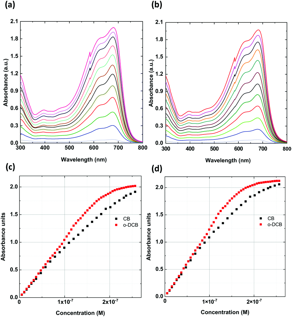 | ||
| Fig. 3 UV-vis spectra of PTB7 in (a) CB and (b) o-DCB for selected concentrations from 5.30 × 10⁻⁹ to 2.81 × 10⁻⁷ M. The calibration curve based on UV-vis absorbance spectra recorded on single bands at (c) 680 nm (d) and 629 nm for different concentrations of PTB7 in CB and o-DCB. | ||
High-pressure spectroscopy
UV-vis spectra of the solid-state PTB7 layers were obtained using a Merrill–Bassett diamond-anvil cell (DAC) equipped with diamond anvils IIA. The PTB7 layers were deposited on the diamond culet through three methods:(i) The PTB7 layer deposited by uniaxial compression: after placing a small amount of the sample on the diamond culet, it was strongly pressed from above by a thick glass plate until it fused into a uniform layer (Fig. 4d).
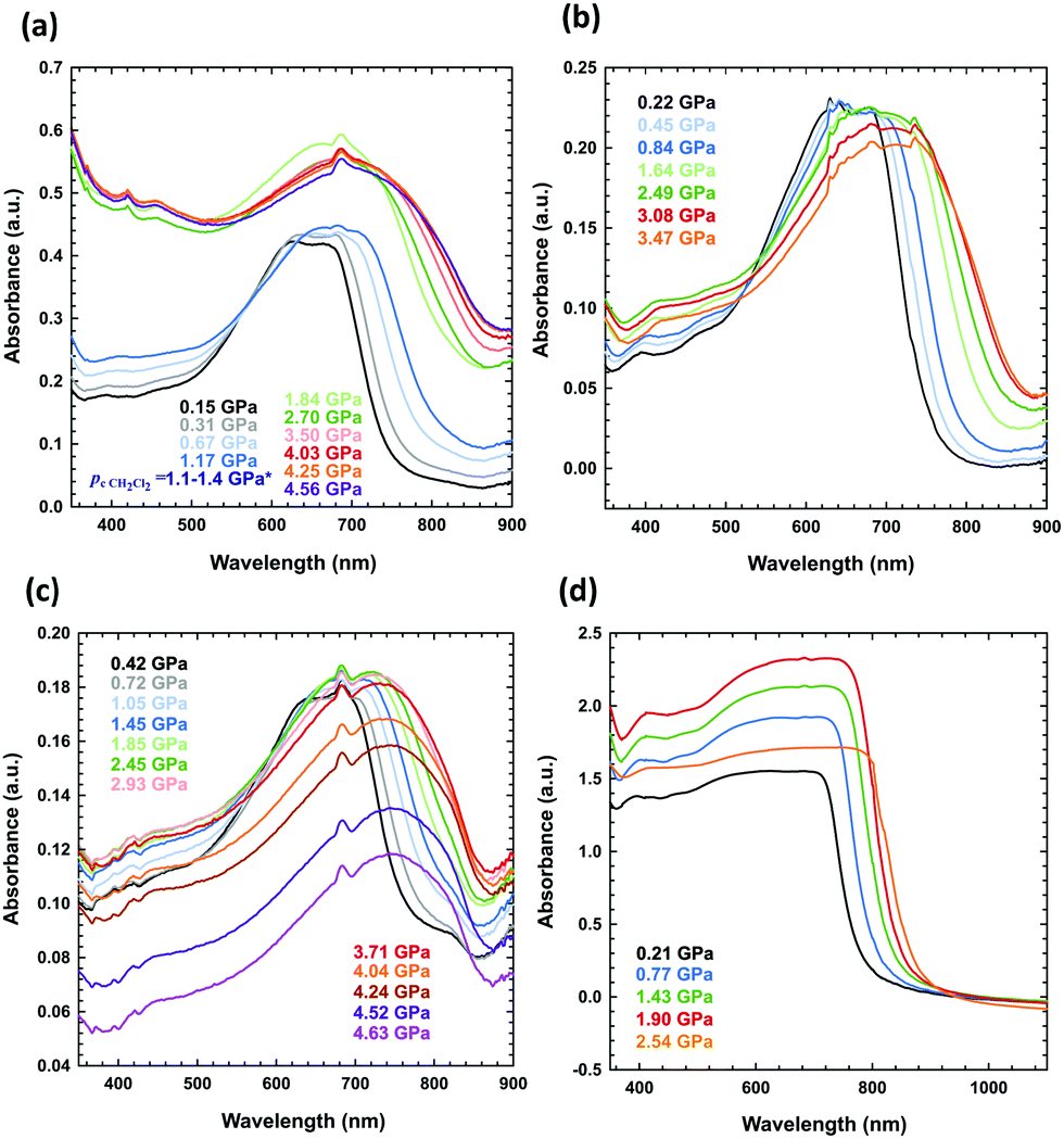 | ||
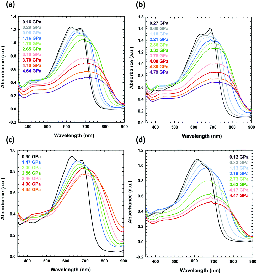
| Fig. 4 High-pressure absorbance spectra of PTB7 measured for (a) a solution of PTB7 in dichloromethane (the sample was liquid up to 1.25 GPa, when dichloromethane freezes at 296 K),61,62 (b) a PTB7 layer on one culet, formed upon evaporation of dichloromethane, (c) the same layer as in (b), but on two diamond culets, and (d) a layer pressed on one culet. | ||
(ii) The PTB7 layer deposited by solvent evaporation: a drop of the PTB7 solution in dichloromethane, chlorobenzene or 1,2-dichlorobenzene was placed on the culet, and the layer was formed after solvent evaporation (Fig. 4b, c and 5).
 | ||
| Fig. 5 High-pressure absorbance spectra of PTB7 layers prepared from the solutions after the evaporation of the following solvents: (a) CB, (b) o-DCB, (c) a CB–DIO mixture, and (d) an o-DCB–DIO mixture. The concentration of each solution was 10 mg mL−1. | ||
(iii) The PTB7 layer deposited by the solution under high pressures: the solution of PTB7 in dichloromethane was loaded into the DAC chamber, and the layer was formed as a precipitate after increasing the pressure (Fig. 4a).
When measuring the absorbance spectrum of PTB7 dissolved in dichloromethane above the freezing pressure of dichloromethane (above 1.25 GPa), a clear jump-like increase was observed in the absorbance (Fig. 4a). This jump is associated with the precipitation of small grains of PTB7 extruded from dichloromethane upon crystallization. The crystallization of the solvent in the DAC chamber is clearly visible through the microscope, but this process significantly increases the scattering of the probing-beam light on the tiny grains of PTB7 dispersed in the sample. We also observed this effect for other freezing solutions.
The UV-vis spectra measured in the DAC for PTB7 layers prepared using different methods (i–iii) display similar strong bathochromic pressure effects (Fig. 6). The absorption edges up to 5 GPa are shifted by approximately 25 nm GPa−1 in the range 700–870 nm. It is a characteristic of all spectra series that, in the initial increased pressure ranges up to approximately 1 GPa, the absorption edge shift is linearly dependent on pressure. Then, above 1 GPa, dλ/dp gradually decreases, and above 4 GPa, dλ/dp is several times smaller compared to that in the range from 0.1 MPa to 1 GPa.
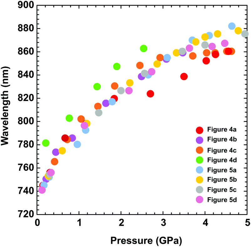 | ||
| Fig. 6 The absorption edge as a function of pressure, depending on the PTB7 preparation method. As described in the plot, the different colours refer to the data in Fig. 4 and 5. | ||
This finding correlates with the tendency of PTB7 to form aggregates, which are known to cause red absorption.54,55 In a photoluminescence study, Hedley et al. revealed that small nanoaggregates of polymer chains can enhance the red absorption range above 600 nm, which they connected to microaggregation.56
Scanning electron microscopy (SEM) images were recorded to inspect the homogeneity of the prepared layers: (i) PTB7 powder compressed into the culet (Fig. S2a in the ESI†) and (ii) a layer formed by evaporation of dichloromethane (Fig. S2b in the ESI†). The SEM images allowed us to determine that the thickness of the layer formed by pressing the powdered product into the diamond was approximately 15 μm. The PTB7 layers formed via solvent evaporation were much thinner. The SEM micrographs show that the surface of the PTB7 layers formed by powder compression is homogenous and uniform, whereas the layers formed by dichloromethane evaporation consist of small patches with gaps and cracks that cause various patterns of defects in the deposited film.
X-ray powder diffraction (XRD) measurements (Fig. S3 in the ESI†) were used to confirm that both samples (i) prepared by pressing PTB7 and (ii) obtained by evaporating the solvent were amorphous.
The heat generated by the electric current in a through-plane thin layer was registered through thermal imaging. The experiment includes thermographic images that were each registered at the end of 3 minute intervals, when a stable state was reached for a constant current and temperature. To assess the electrical and thermal behaviours of PTB7 compounds, the change in the thermal signature was registered while applying an external potential. Two devices were constructed with the following configurations: (a) glass/ITO/PTB7/Ag/ITO/glass and (b) PET/ITO/PTB7/Ag/ITO/PET. These configurations differ based on the glass and PET substrates. In both devices, the thin PTB7 layers display nearly linear current-to-voltage dependences (Fig. 7), which confirms that the polymer is an electric conductor. The electric resistance of glass-supported PTB7 was 178.5 Ω and that of PET-supported PTB7 was 119.1 Ω. The difference is related to the pixeled glass support giving a longer conductive pathway than in the case of the PET/ITO support. However, for PET-supported PTB7, the lower resistance resulted in a larger current, causing a higher temperature, which in turn led to a drastic decline in the current above 6 V/136 °C. Nevertheless, high temperatures observed in the thermal images suggest the progressive degradation of the device, although at a lower pace.
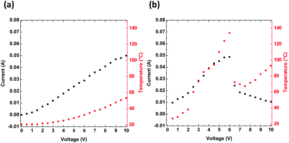 | ||
| Fig. 7 Electric current (black) and temperature (red) as a function of applied voltage for devices composed of (a) glass/ITO/PTB7/Ag/ITO/glass and (b) PET/ITO/PTB7/Ag/ITO/PET. | ||
The thermal response, culminating at approximately 53 °C for glass devices and at 136 °C for PET-supported PTB7 devices, shows an approximate logarithmic dependence on the voltage. For the flexible support, a higher temperature affects the organic layers and reduces their performance. According to the thermal images (Fig. 8), the edges of the device are most affected and overheated compared to the other regions. Defects located along the edges are most likely the cause of overheating and subsequent degradation of the PTB7 layers. In the present form, the PET-supported device performs well up to approximately 5 V.
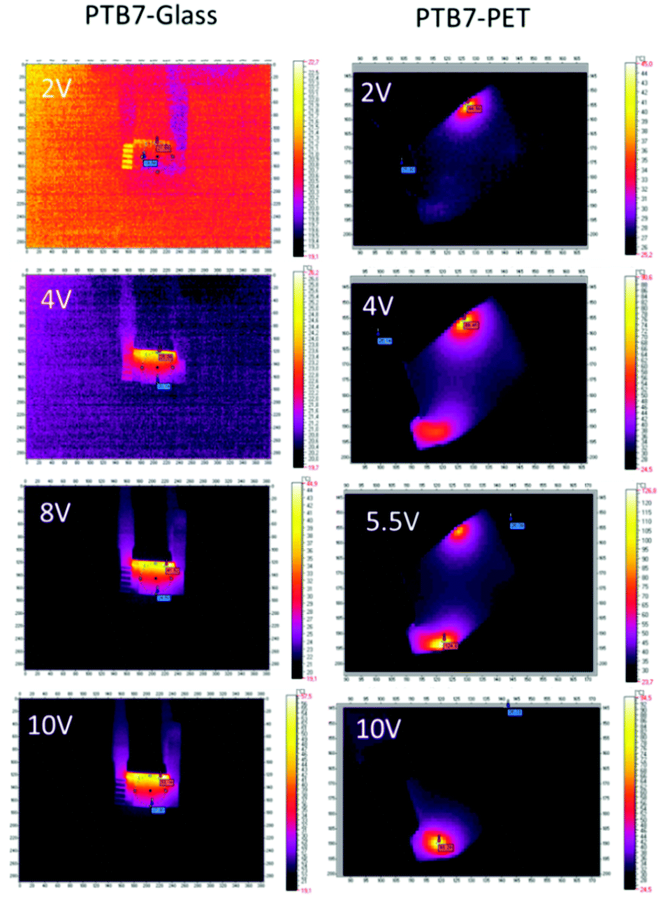 | ||
| Fig. 8 Thermal images for glass/ITO/PTB7/Ag/ITO/glass and PET/ITO/PTB7/Ag/ITO/PET devices. | ||
Thermally induced pressure effect on the energy gap in PTB7
The thermal expansion of the PTB7 layers can generate compression due to the smaller thermal expansion of the substrate. The pressure (Δp) required to compensate for the difference in the dimensions of the PTB7 layer and the glass substrate can be assessed using the formula Δp = ΔL·K/3, where K is the difference between the bulk moduli of PTB7 and glass and ΔL is the difference in the linear dimensions of the PTB7 layer and the glass substrate. These approximate calculations result in Eg changes of 10−4 eV K−1. Thus, a temperature change of 100 K would result in the narrowing of the PTB7 bandgap by 0.1 eV in the glass substrate device.Mechanical properties
An important property of materials that are used to build elastic organic devices is their resistance to mechanical deformations. We have studied the mechanical properties of samples composed of a layered structure of poly(ethylene-terephthalate) (PET), indium-tin oxide (ITO) and PTB7. We prepared the devices by coating single and double layers of PTB7 through the spin coating technique. The samples were 0.17 mm thick. The selected mechanical properties of these devices are summarized in Fig. 9 and Table S1 in the ESI.† The devices break under the average stress values of 93(8) MPa for the single-layer and 155(8) MPa for the double-layer PTB7 versions. The maximum elongations before breaking, equal to ΔLmax/Lo × 100%, were (113 ± 38)% and (111 ± 14)% for single and double layers of PTB7, respectively.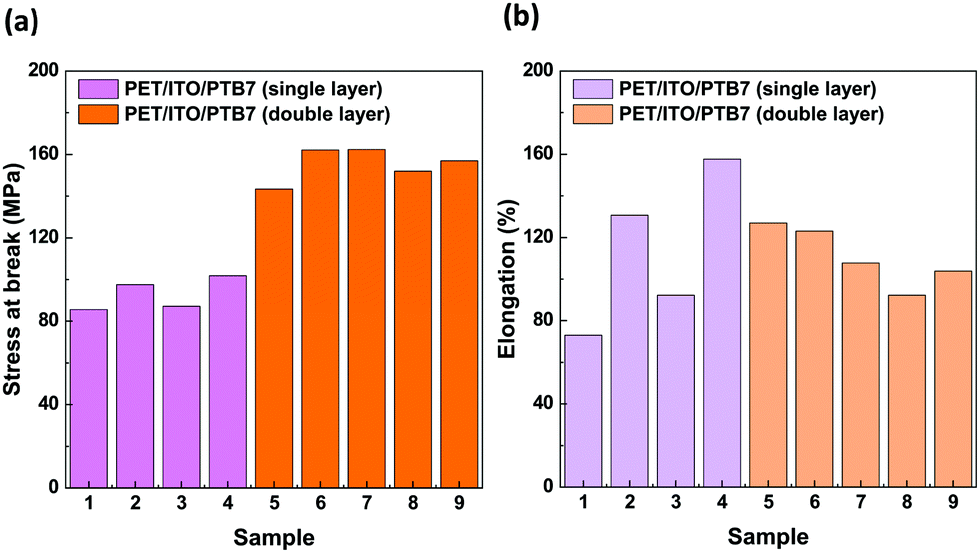 | ||
| Fig. 9 (a) Stress at break and (b) elongation at break for PET/ITO/PTB7 single layer (samples no. 1–4) and double layer (no. 5–9) devices. | ||
The correlation between the stretching force and elongation (Fig. 10) drastically differs for the single- and double-coated PET/ITO samples in the multilayer substrate devices. For all samples, the tests revealed both elastic and plastic behaviours, with the transition reaching approximately 2 mm elongation (approximately 0.8% of the initial length) at a force of approx. 135 N (79 MPa), consistent with the elastic properties of the PET/ITO support. After reaching the transition, the PTB7 single-coated samples became fully plastic and elongated until they broke with a negligible increase in the applied force. The plastic deformations of the samples with double-layer PTB7 clearly differed from those with the single layer. The force–elongation dependence for double-layer PTB7 deviated from the typical plastic behaviour due to the effect of the approximately 100 N force enhancement that occurred before reaching the break point. This shows that the double layer of PTB7 adds an elastic component to the typical plastic behaviour, increasing the value of the applied force and the value of the stress at the breaking point. The PTB7 double layer reduced the breaking-point elongation to an average value of 29.3 mm (samples 5–9) compared to an average value of 37 mm for the PTB7 single-layer samples 2 and 4. This change is connected to the higher values of the stretching force and the breaking point for the PTB7 double-layer samples (on average 250 N) compared to the PTB7 single-layer samples (150 N). However, the PTB7 single-layer samples 1 and 3 broke at the lowest elongation values of 19 and 25 mm, respectively. In the case of the 5th sample, a slight deviation from the normal behaviour was attributed to the imperfection of the PET/ITO support probably caused by the cutting process.
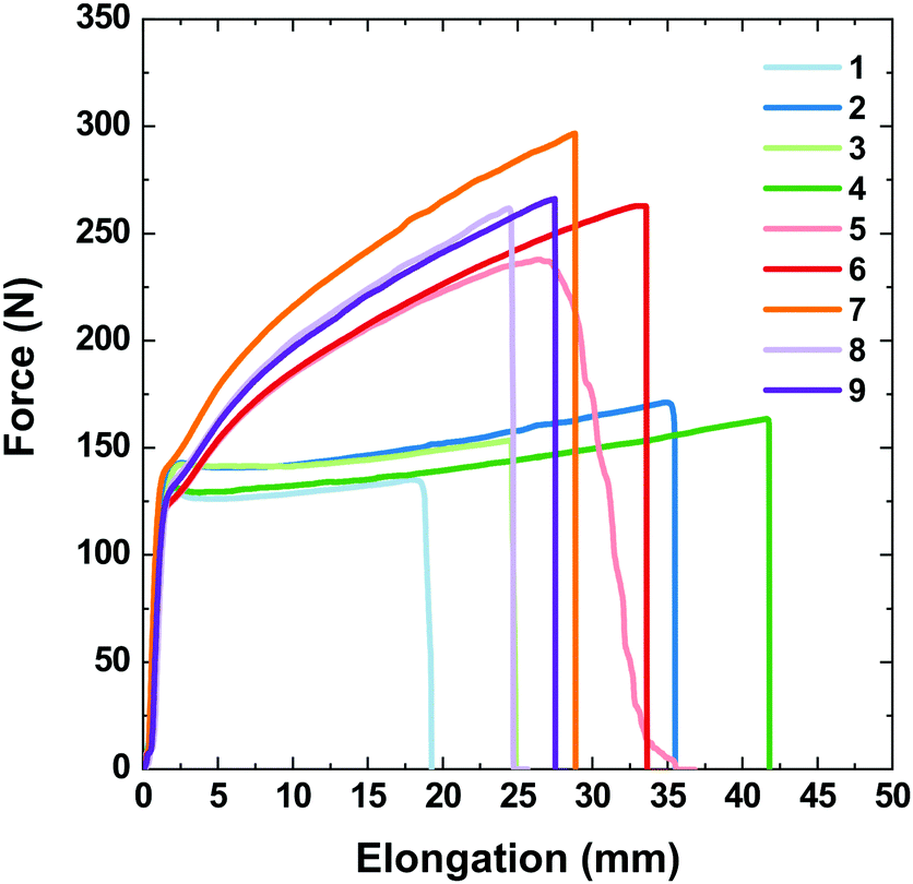 | ||
| Fig. 10 Stretching force values as a function of elongation for PET/ITO/PTB7 single layer (samples 1–4) and double layer (5–9) devices. | ||
Experimental
Materials
Poly[[4,8-bis[(2-ethylhexyl)oxy]benzo[1,2-b:4,5b′]dithiophene-2,6-diyl][3-fluoro-2-[(2-ethylhexyl)carbonyl]thieno[3,4b]thiophenediyl]], commonly abbreviated as PTB7, was purchased from Ossila Ltd (Sheffield, UK). Solvents and 1,8-diiodooctane (DIO) were of reagent grade and were obtained from Aldrich Chemical Co. (Saint Louis, MO, USA).Methods
High-pressure experiments were performed using a Merrill–Bassett diamond-anvil cell (DAC)57 modified by mounting the diamond anvils directly on steel backing supports with conical windows. The gasket was made of 0.1 mm thick tungsten foil or steel with sparked-eroded holes of 0.4 to 0.5 mm in diameter. The gaskets were preindented to 0.05 mm. The pressure was calibrated using the ruby fluorescence method.58,59 The ultraviolet-visible (UV-vis) spectra of PTB7 at high pressure were recorded using Jasco V-650 and Jasco V-770 spectrophotometers adapted for using a DAC. The absorbance was measured at a scan speed of 200 nm min−1 in the 350–1100 nm or 350–900 nm range. In compression experiments, the pressure-transmitting medium was glycerol.The basic transmission UV-vis spectra of PTB7 in solution were acquired using an A360 UV–Vis spectrophotometer (AOR Instruments, Shanghai, China) with an interval of 0.2 nm and medium scan speed in the range of 200 nm to 800 nm.
Scanning electron microscopy (SEM) images for the two layers, (i) PTB7 powder compressed into the culet and (ii) formed by evaporation of dichloromethane, were investigated using a Zeiss EVO 40 scanning electron microscope.
The PTB7 sample and the sample after evaporation of 1,2-dichlororobenzene were characterized under ambient conditions by X-ray powder diffraction (XRD). A Bruker AXS D8 diffractometer equipped with a Johansson monochromator selecting the Cu Kα1 line was used (λ = 1.54060 Å). Silicon single-crystal plates were used as the sample cuvette to reduce the background.
The thermal behaviour was observed upon the application of a potential using a thermographic camera (VIGOcam v50, VIGO System S. A., Ożarów Mazowiecki, Poland) and a multichannel potentiostat–galvanostat (PGStat Autolab M101, Metrohm, Barendrecht, Nederland) as described in detail elsewhere.60 The samples were prepared through the spin casting method with the PTB7 solution (10 mg mL−1 in chlorobenzene) on ITO-coated PET or the glass support (900 rpm, 30 s). Additionally, to improve the electric contact, a layer of silver paste was used to bind the electrode separated from the sample.
The mechanical properties (tensile strain) were investigated using an Instron 33R4469 (Instron, Norwood, MA, USA) testing machine with a load cell of 5 kN, and the results were registered using the Bluehill 3.0 software (Instron, Norwood, MA, USA). The PTB7 solution (10 mg mL−1 in chlorobenzene) was spun cast (900 rpm, 30 s) on a 5 × 5 cm2 ITO-coated PET support. For mechanical tests, 5 × 1 cm2 plates were used.
Conclusions
We have performed complex experiments aimed at determining the performance of PTB7 layers in flexible photovoltaic devices using both glass and PET substrates. The PTB7 polymer, an efficient donor material for photovoltaic devices, displays a bathochromic shift in the absorption edge and Eg energy gap narrowing under high pressure, both in solution and in the solid state. Different concentrations of PTB7 dissolved in chlorobenzene and o-chlorobenzene and solid layers prepared through different methods were investigated. The disordered arrangement of polymer agglomerates starts at concentrations above 1.81 × 10⁻⁷ M (2.28 × 10⁻² mg mL−1) and is more evident for the o-DCB solution due to the higher dipole moment of o-DCB molecules. The high pressure measurements for the films formed by evaporating the solutions in dichloromethane, chlorobenzene and o-dichlorobenzene, both without and with the addition of DIO, demonstrate that the redshift in the range of 740–880 nm is approximately 25 nm GPa−1. Both spectroscopic studies in the UV-vis range provided evidence of PTB7 ordering and two-step aggregation. In solution, only the concentration-dependent disordering of the polymers was observed, whereas the pressure-induced aggregation appears more favourable for disordering macroscopic aggregates and polymeric side-chain aggregation (nanoaggregation), which more efficiently compensate for the external force. Both the PET- and glass-supported PTB7 layers have similar electrical conductivities and performances up to 6 V. However, for higher current, the PET-supported samples degrade at locations starting from point defects when the temperature reaches 140 °C. The mechanical performance of the flexible PET/ITO support is nearly identical for single- and double PTB7 layers in the elastic region up to 0.8% elongation. However, this performance shows significant differences in both the plastic deformation and breaking point values of 93.1 ± 7.9 MPa and 155.4 ± 7.9 MPa, respectively. This result demonstrates that the resistance to mechanical and electrical damage can be substantially improved by depositing additional layers. However, the number of layers does not affect the elastic region of the stress–strain behaviour.Author contributions
Paulina Ratajczyk: investigation, visualization and writing (original draft); Andrzej Katrusiak: writing (original draft), supervision, writing (reviewing and editing), and conceptualization; Krzysztof Artur Bogdanowicz: investigation, visualization, analyses, and writing (original draft); Wojciech Przybyl: investigation; Piotr Krysiak: investigation and analyses; Anna Kwak: investigation; Agnieszka Iwan: writing (original draft), supervision, conceptualization, and writing (reviewing and editing).Conflicts of interest
All authors have read and agreed to the published version of the manuscript.Acknowledgements
The authors are grateful for financial support from the Polish National Centre of Research and Development (TECHMATSTRATEG1/347431/14/NCBR/2018) and from the Polish Ministry of Education and Science within the Diamentowy Grant DI2019 0160 49. The authors would like to thank Ms B. Jewloszewicz for conducting the UV-vis experiment.Notes and references
- M. Riede, D. Spoltore and K. Leo, Adv. Energy Mater., 2021, 11, 2002653 CrossRef CAS.
- J. D. Roehling, D. Baran, J. Sit, T. Kassar, T. Ameri, T. Unruh, C. J. Brabec and A. J. Moulé, Sci. Rep., 2016, 6, 30915 CrossRef CAS PubMed.
- C. Zhong, V. K. Sangwan, C. Wang, H. Bergeron, M. C. Hersam and E. A. Weiss, J. Phys. Chem. Lett., 2018, 9, 2484–2491 CrossRef CAS PubMed.
- Z. Zhang, J. Miao, Z. Ding, B. Kan, B. Lin, X. Wan, W. Ma, Y. Chen, X. Long, C. Dou, J. Zhang, J. Liu and L. Wang, Nat. Commun., 2019, 10, 3271 CrossRef PubMed.
- J. Miao, Y. Wang, J. Liu and L. Wang, Chem. Soc. Rev., 2022, 51, 153–187 RSC.
- Y. Wang, W. Xu, J. Yi, C. Zuo, Y. Gong, Y. Liu, W. Y. Lai and W. Huang, J. Mater. Chem. A, 2018, 6, 15977–15984 RSC.
- L. Duan and A. Uddin, Adv. Sci., 2020, 7, 1903259 CrossRef CAS PubMed.
- Y. Wang, B. Wu, Z. Wu, Z. Lan, Y. Li, M. Zhang and F. Zhu, J. Phys. Chem. Lett., 2017, 8, 5264–5271 CrossRef CAS PubMed.
- C. Yang, Y. Sun, Q. Li, K. Liu, X. Xue, Y. Huang, K. Ren, L. Li, Y. Chen, Z. Wang, S. Qu and Z. Wang, J. Phys. Chem. Lett., 2020, 11, 927–934 CrossRef CAS PubMed.
- H. Chen, J. Qu, L. Liu, W. Chen and F. He, J. Phys. Chem. Lett., 2019, 10, 936–942 CrossRef CAS PubMed.
- C. K. Lyu, F. Zheng, B. H. Babu, M. S. Niu, L. Feng, J. L. Yang, W. Qin and X. T. Hao, J. Phys. Chem. Lett., 2018, 9, 6238–6248 CrossRef CAS PubMed.
- S. Karuthedath, J. Gorenflot, Y. Firdaus, N. Chaturvedi, C. S. P. De Castro, G. T. Harrison, J. I. Khan, A. Markina, A. H. Balawi, T. A. Dela Peña, W. Liu, R. Z. Liang, A. Sharma, S. H. K. Paleti, W. Zhang, Y. Lin, E. Alarousu, D. H. Anjum, P. M. Beaujuge, S. De Wolf, I. McCulloch, T. D. Anthopoulos, D. Baran, D. Andrienko and F. Laquai, Nat. Mater., 2021, 20, 378–384 CrossRef CAS PubMed.
- Y. Gong, J. Zhang, B. Du, M. Wang, W. Y. Lai and W. Huang, ACS Appl. Electron. Mater., 2019, 1, 854–861 CrossRef CAS.
- X. Li, H. Wang, H. Nakayama, Z. Wei, J. A. Schneider, K. Clark, W. Y. Lai, W. Huang, J. G. Labram, J. R. De Alaniz, M. L. Chabinyc, F. Wudl and Y. Zheng, ACS Appl. Energy Mater., 2019, 2, 3805–3814 CrossRef CAS.
- K. Fukuda, K. Yu and T. Someya, Adv. Energy Mater., 2020, 10, 2000765 CrossRef CAS.
- D. Koo, S. Jung, J. Seo, G. Jeong, Y. Choi, J. Lee, S. M. Lee, Y. Cho, M. Jeong, J. Lee, J. Oh, C. Yang and H. Park, Joule, 2020, 4, 1021–1034 CrossRef CAS.
- Y. Sun, T. Liu, Y. Kan, K. Gao, B. Tang and Y. Li, Small Sci., 2021, 1, 2100001 CrossRef.
- L. Lu and L. Yu, Adv. Mater., 2014, 26, 4413–4430 CrossRef CAS PubMed.
- X. Y. Liu, W. K. Chen, W. H. Fang and G. Cui, J. Phys. Chem. Lett., 2019, 10, 2949–2956 CrossRef CAS PubMed.
- G. Dennler, M. C. Scharber, T. Ameri, P. Denk, K. Forberich, C. Waldauf and C. J. Brabec, Adv. Mater., 2008, 20, 579–583 CrossRef CAS.
- H. Chen, R. Zhang, X. Chen, G. Zeng, L. Kobera, S. Abbrent, B. Zhang, W. Chen, G. Xu, J. Oh, S. H. Kang, S. Chen, C. Yang, J. Brus, J. Hou, F. Gao, Y. Li and Y. Li, Nat. Energy, 2021, 6, 1045–1053 CrossRef CAS.
- T. Wu, Z. Qin, Y. Wang, Y. Wu, W. Chen, S. Zhang, M. Cai, S. Dai, J. Zhang, J. Liu, Z. Zhou, X. Liu, H. Segawa, H. Tan, Q. Tang, J. Fang, Y. Li, L. Ding, Z. Ning, Y. Qi, Y. Zhang and L. Han, Nano-Micro Lett., 2021, 13, 152 CrossRef CAS PubMed.
- H. Bin, J. Wang, J. Li, M. M. Wienk and R. A. J. Janssen, Adv. Mater., 2021, 33, 2008429 CrossRef CAS PubMed.
- D. Li, W. Y. Lai, Y. Z. Zhang and W. Huang, Adv. Mater., 2018, 30, 1704738 CrossRef PubMed.
- T. Cheng, Y. Zhang, W. Y. Lai and W. Huang, Adv. Mater., 2015, 27, 3349–3376 CrossRef CAS PubMed.
- L. Duan, B. Hoex and A. Uddin, Sol. RRL, 2021, 5, 2100041 CrossRef CAS.
- A. Iwan, W. Pellowski and K. A. Bogdanowicz, Energies, 2021, 14, 6186 CrossRef CAS.
- L. Wang, S. Zhao, Z. Xu, J. Zhao, D. Huang and L. Zhao, Materials, 2016, 9, 171 CrossRef PubMed.
- Z. He, C. Zhong, S. Su, M. Xu, H. Wu and Y. Cao, Nat. Photonics, 2012, 6, 591–595 CrossRef.
- K. Lang, Q. Guo, Z. He, Y. Bai, J. Yao, M. Wakeel, M. S. Alhodaly, T. Hayat and Z. Tan, J. Phys. Chem. Lett., 2020, 11, 9596–9604 CrossRef CAS PubMed.
- I. P. Murray, S. J. Lou, L. J. Cote, S. Loser, C. J. Kadleck, T. Xu, J. M. Szarko, B. S. Rolczynski, J. E. Johns, J. Huang, L. Yu, L. X. Chen, T. J. Marks and M. C. Hersam, J. Phys. Chem. Lett., 2011, 2, 3006–3012 CrossRef CAS.
- D. Zhang, R. Hu, J. Cheng, Y. Chang, M. Huo, J. Yu, L. Li and J. P. Zhang, Polymers, 2018, 10, 332 CrossRef PubMed.
- S. Park, J. Jeong, G. Hyun, M. Kim, H. Lee and Y. Yi, Sci. Rep., 2016, 6, 35262 CrossRef CAS PubMed.
- Z. Jin, D. Gehrig, C. Dyer-Smith, E. J. Heilweil, F. Laquai, M. Bonn and D. Turchinovich, J. Phys. Chem. Lett., 2014, 5, 3662–3668 CrossRef CAS PubMed.
- N. Zarrabi, P. L. Burn, P. Meredith and P. E. Shaw, J. Phys. Chem. Lett., 2016, 7, 2640–2646 CrossRef CAS PubMed.
- V. Savikhin, L. K. Jagadamma, L. J. Purvis, I. Robertson, S. D. Oosterhout, C. J. Douglas, I. D. W. Samuel and M. F. Toney, iScience, 2018, 2, 182–192 CrossRef CAS PubMed.
- J. Kettle, Z. Ding, M. Horie and G. C. Smith, Org. Electron., 2016, 39, 222–228 CrossRef CAS.
- U. N. V. Huynh, T. P. Basel, E. Ehrenfreund and Z. V. Vardeny, J. Phys. Chem. Lett., 2018, 9, 4544–4549 CrossRef CAS PubMed.
- M. Szafrański and A. Katrusiak, J. Phys. Chem. Lett., 2016, 7, 3458–3466 CrossRef PubMed.
- A. Jaffe, Y. Lin and H. I. Karunadasa, ACS Energy Lett., 2017, 2, 1549–1555 CrossRef CAS.
- P. Postorino and L. Malavasi, J. Phys. Chem. Lett., 2017, 8, 2613–2622 CrossRef CAS PubMed.
- X. Lü, W. Yang, Q. Jia and H. Xu, Chem. Sci., 2017, 8, 6764–6776 RSC.
- M. Szafrański and A. Katrusiak, J. Phys. Chem. Lett., 2017, 8, 2496–2506 CrossRef PubMed.
- M. Coduri, T. A. Strobel, M. Szafrański, A. Katrusiak, A. Mahata, F. Cova, S. Bonomi, E. Mosconi, F. De Angelis and L. Malavasi, J. Phys. Chem. Lett., 2019, 10, 7398–7405 CrossRef CAS PubMed.
- G. Liu, L. Kong, W. Yang and H. Mao, Mater. Today, 2019, 27, 91–106 CrossRef CAS.
- L. Zhang, Y. Fang, L. Sui, J. Yan, K. Wang, K. Yuan, W. L. Mao and B. Zou, ACS Energy Lett., 2019, 4, 2975–2982 CrossRef CAS.
- S. Jiang, Y. Fang, R. Li, H. Xiao, J. Crowley, C. Wang, T. J. White, W. A. Goddard, Z. Wang, T. Baikie and J. Fang, Angew. Chem., 2016, 128, 6650–6654 CrossRef.
- F. Aguado, F. Rodríguez, R. Valiente, J. P. Itiè and M. Hanfland, Phys. Rev. B: Condens. Matter Mater. Phys., 2012, 85, 100101 CrossRef.
- Y. Lee, D. B. Mitzi, P. W. Barnes and T. Vogt, Phys. Rev. B: Condens. Matter Mater. Phys., 2003, 68, 020103 CrossRef.
- F. Capitani, C. Marini, S. Caramazza, P. Postorino, G. Garbarino, M. Hanfland, A. Pisanu, P. Quadrelli and L. Malavasi, J. Appl. Phys., 2016, 119, 185901 CrossRef.
- G. Liu, L. Kong, J. Gong, W. Yang, H. Mao, Q. Hu, Z. Liu, R. D. Schaller, D. Zhang and T. Xu, Adv. Funct. Mater., 2017, 27, 1604208 CrossRef.
- C. Zhu, X. Niu, Y. Fu, N. Li, C. Hu, Y. Chen, X. He, G. Na, P. Liu, H. Zai, Y. Ge, Y. Lu, X. Ke, Y. Bai, S. Yang, P. Chen, Y. Li, M. Sui, L. Zhang, H. Zhou and Q. Chen, Nat. Commun., 2019, 10, 815 CrossRef CAS PubMed.
- G. H. Ahn, M. Amani, H. Rasool, D. H. Lien, J. P. Mastandrea, J. W. Ager, M. Dubey, D. C. Chrzan, A. M. Minor and A. Javey, Nat. Commun., 2017, 8, 608 CrossRef PubMed.
- Y. Liang, Z. Xu, J. Xia, S. T. Tsai, Y. Wu, G. Li, C. Ray and L. Yu, Adv. Mater., 2010, 22, 135–138 CrossRef PubMed.
- D. Wang, Y. Yuan, Y. Mardiyati, C. Bubeck and K. Koynov, Macromolecules, 2013, 46, 6217–6224 CrossRef CAS.
- G. J. Hedley, F. Steiner, J. Vogelsang and J. M. Lupton, J. Phys. Chem. Lett., 2017, 8, 3494–3499 CrossRef CAS PubMed.
- L. Merrill and W. A. Bassett, Rev. Sci. Instrum., 1974, 45, 290–294 CrossRef.
- G. J. Piermarini, S. Block, J. D. Barnett and R. A. Forman, J. Appl. Phys., 1975, 46, 2774–2780 CrossRef CAS.
- H. K. Mao, J. Xu and P. M. Bell, J. Geophys. Res., 1986, 91, 4673 CrossRef CAS.
- A. Rózycka, K. A. Bogdanowicz, N. Górska, J. Rysz, M. Marzec, A. Iwan, R. Pich and A. Januszko, Materials, 2019, 12, 1097 CrossRef PubMed.
- M. Podsiadło, K. Dziubek and A. Katrusiak, Acta Crystallogr., Sect. B: Struct. Sci., 2005, 61, 595–600 CrossRef PubMed.
- D. Kurzydłowski, T. Chumak and J. Rogoża, Crystals, 2020, 10, 920 CrossRef.
Footnote |
| † Electronic supplementary information (ESI) available. See DOI: 10.1039/d1ma01066b |
| This journal is © The Royal Society of Chemistry 2022 |