 Open Access Article
Ocean wave energy generator based on graphene/TiO2 nanoparticle composite films†
Han
Xue
a,
Haomin
Liu
a,
Viktoriia
Mishukova
 a,
Bo
Xu
 b and
Jiantong
Li
 *a
*a
aKTH Royal Institute of Technology, School of Electrical Engineering and Computer Science, Electrum 229, 16440 Kista, Sweden. E-mail: jiantong@kth.se
bMIIT Key Laboratory of Advanced Display Materials and Devices, Institute of Optoelectronics & Nanomaterials, School of Materials Science and Engineering, Nanjing University of Science and Technology, Nanjing, 210094, China
First published on 16th February 2022
Abstract
Harvesting ocean wave energy through carbon-based materials, particularly graphene, is receiving increasing attention. However, the complicated fabrication process and the low output power of the present monolayer graphene-based wave energy generators limit their further application. Here, we demonstrate the facile fabrication of a new type of wave energy generator based on graphene/TiO2 nanoparticle composite films using the doctor-blading method. The developed wave energy harvesting device exhibits a high open-circuit voltage of up to 75 millivolts and a high output power up to 1.8 microwatts. A systematic study was conducted to explore the optimal conditions for the energy harvesting performance.
The ocean that covers nearly 72% of the Earth's surface is abundant in enormous energy in a variety of forms including heat, currents, waves, and tides.1 Harvesting this kind of renewable energy is regarded as a promising approach to deal with the global concern of energy shortage. Among the various forms of ocean energy, ocean wave power is stable, predictable, and plentiful. It can be harvested all the time: day and night under varying weather conditions.2 The present wave energy conversion techniques rely on bulky equipment that cause engineering and economic challenges,3 and bring biological and/or physical impacts to the marine environment,4 which calls for facile and sustainable ways to achieve wave energy harvesting. Recently, a new, simple, yet promising wave energy conversion technique has been demonstrated through extracting wave potential directly from the interaction between graphene and a dynamic salt water–air interface.5 The 2D molecular structure and richness of active π electrons6 endow graphene with high electrical conductivity (∼106 S cm−1),7 large charge carrier mobility (2 × 105 cm2 V−1 s−1),7 and good sensitivity to external cations/ions in salted water,8,9 turning it into an ideal material for energy conversion.10 When a graphene-covered substrate makes contact with a salt solution, an electric double layer (EDL) is formed at the graphene–solution interface.11–14 In particular, the movement of the liquid–gas interface (such as the ocean waves) may cause an imbalance between absorbed ions at the graphene surface and the counterions in the liquid, resulting in an instantaneous net charge. The charge inclines to draw electrons from graphene, leading to an electric potential and current across the graphene sheet that can be directly harvested as electricity.8,15 Extensive efforts and achievements have been made on wave power harvesting using graphene and graphene derivatives through this method.16–20 However, there are still a few issues limiting further development. As reported, most graphene-based wave energy generators rely on large-area monolayer graphene by the chemical vapor deposition (CVD) technique,5,19,21 followed by transferring to the target substrates.5,15 The expensive and complicated fabrication procedure and inevitable cracks on the transferred graphene inhibit it for mass production. In particular, it is critical to control the graphene thickness to monolayer because multilayer graphene exhibits diminishing voltage due to decreased resistance.22 Although the collected potential of monolayer graphene is limited to only several (<10) millivolts with negligible currents. Recently, simple and cost-effective wave energy generators based on graphene/carbon black/polymer composite films have been demonstrated with a maximum output voltage around 20 mV and a maximum current of about 10 μA.18
In this study, we demonstrate a facile process to fabricate wave energy generators based on graphene nanosheets/TiO2 nanoparticle composite films. Multilayer (mostly 3–6 layers)23 graphene nanosheets are prepared through the efficient and low-cost electrochemical exfoliation process, following our previous work.23,24 In order to improve the low wave potential of multilayer graphene as observed in other research, insulating TiO2 nanoparticles are introduced to the composites to reduce their conductivity. The low conductivity of the composite films allows slow response to the ion balance,25 so as to improve their harvesting ability. As a result, the graphene/TiO2 composite-based device can readily generate an open-circuit voltage up to 75 mV, a short-circuit current up to 25 μA, and a maximum output power around 1.8 μW.
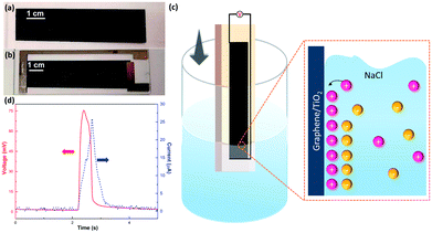
The bladed graphene/TiO2 film (thickness around 6 μm, Fig. S1†) and final wave energy generator are shown in Fig. 1a and b. A pure TiO2 film was also bladed onto a glass substrate as a reference, showing transparent appearance (Fig. S2a†). The Raman spectrum (Fig. S3†) indicates the characteristic Eg band of TiO2 and the D band, G band and 2D band of graphene, confirming the existence of both TiO2 and graphene in the film.
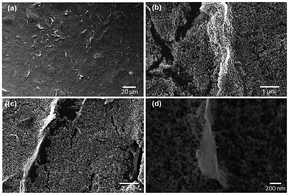
Fig. 1c illustrates our experimental setup. The sample connected with a multimeter was cyclically inserted into and pulled out of a 0.6 M NaCl solution at a constant velocity and within the range of insertion depth. Fig. 1d shows one representative electric voltage signal observed during the dynamic process. An increasing positive voltage was obtained when the sample was inserted into the solution until a peak voltage of 75 mV was reached at the maximum insertion depth, followed by a dramatic drop when the sample was pulled out. Accordingly, the short-circuit current signal also indicates a peak with the maximum current of 25 μA, suggesting an output power of 1.8 μW. In contrast, the pure TiO2 sample is electrically insulating, and no evident open-circuit voltage can be observed when it moved either in the air or in the salt solution under the same test conditions (Fig. S2†). On the other hand, however, the pure graphene film (fabricated through inkjet printing), exhibits a low wave potential of ∼5 mV (Fig. S4†). These suggest the importance of the combining graphene and TiO2 nanoparticles. As shown by the SEM images in Fig. 2, in the graphene/TiO2 films, the majority of graphene is buried by the TiO2 nanoparticles with some of them partly exposed. Owing to the presence of TiO2 nanoparticles, the electrical conductivity of graphene can be adjusted to a low levels. According to a previous study,25 a low conductivity leads to slow charge carrier mobility inside the material and thus elevates the potential, improving the wave energy harvesting performance. The exposed part of graphene is expected to interact with the solution to form the EDL and hence produce the local potential. It is worth noting that the EDL itself is not sufficient for the generation of wave potential. According to the literature,8 a “dynamic” EDL boundary near the liquid–gas interface (Fig. 1c) is necessary for producing the voltage. During our measurement, when the sample was fully immersed in the salt water, no induced voltage was observed. Instead, a significant long-time decay appeared under complete immersion (Fig. S5†), exhibiting typical behavior of resistance–capacitor (RC) circuits,25 and confirming the EDL model as the reasonable mechanism for the wave potential. Even when the sample moved at the same velocity after being immersed fully in the solution, no apparent peak voltages were collected due to the absence of the liquid–gas interface (Fig. S6†). When the sample was pulled out of the salted water, the induced voltage dropped to zero immediately (Fig. S5 and S6†), further demonstrating the necessity of the gas–liquid interface.
Fig. 3 displays the output of the wave energy generators under multiple cycles of inserting and pulling at a constant velocity and interval time of 1 cm s−1 and 10 s, respectively. The open-circuit voltage is pretty stable, varying within a small range between 15 mV and 20 mV (Fig. 3a), about 6 times higher than monolayer graphene,5 achieved at a comparable low velocity. Moreover, the short-circuit current remained around 20 μA (Fig. 3b). As a result, under such low velocity, the maximum output power could reach up to 430 nW (Fig. 3c), comparable with previous devices based on the graphene/carbon black/polymer composite,16 wrinkled graphene,21etc. (for more information, see Table S1†). In addition, even after 200 inserting–pulling cycles (Fig. S7†), the induced potential still retained at the same level as the first time, exhibiting excellent stability.
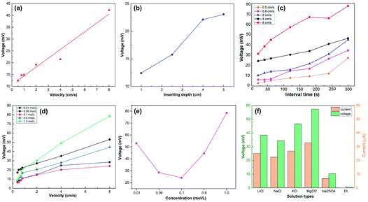
A previous study5 revealed the dependence of the wave potential Von the insertion velocity v, insertion depth d, discharging charge per unit area q0 and sheet resistance of the generator Rsq as  In our study, the velocity ranged from 0.5 cm s−1 to 8 cm s−1, while the interval time was kept constant (10 s) for every velocity. As shown in Fig. 4a, our results confirm that the peak voltage increased linearly with the insertion velocity. According to previous studies,5,25 the large voltage increases at high insertion velocity can be interpreted by the short response time for counterions in the solution to migrate to the dynamic EDL boundary, thus increasing the net charge. The insertion depth indicated a similar behavior as velocity. Fig. 4b revealed that, with continuous insertion into solution, the recorded voltage across the sample increased linearly. The linear increment of induced voltage on inserting depth could be explained by the equally connected resistances assumption.5 The length of the EDL region is divided into several equal sections with the same resistance. An increase in the insertion depth allows more sections to interact with the solution, which increases the total resistance and thus the wave potential.
We further investigated the dependence of the wave potential on the interval time between two inserting–pulling cycles. As shown in Fig. 4c, the peak voltage increases steadily with the interval time at the same velocity. In our experiments, a high interval time (300 s) produced voltage 2–3 times higher than low interval time (10 s). This can be attributed to the wettability of the sample surface. When the movement is within a short interval, due to the hydrophilicity of the film, the wetted surface did not have enough time to recover, severely limiting the region for the dynamic EDL boundary, causing a much lower peak voltage. On the contrary, when the interval time was long enough, the wetted surface became dry again, recovering the region for the dynamic EDL boundary, thus producing a higher voltage. Taking both the insertion velocity and interval time into account, higher velocity exhibited stronger dependence on the interval time since the voltage increase at the highest insertion velocity of 8 cm s−1 was relatively larger than that at lower insertion velocities (Fig. 4c).
The influence of the salt concentration on the peak voltage under the same interval time is revealed in Fig. 4d and e. The concentration of 0.1 M is a delimitation for the voltage dependence on the concentration. As illustrated in Fig. 4e, when the concentration is below 0.1 M, the peak voltage decreases significantly with the increasing concentration. This is consistent with the observation in the literature25 and could be ascribed to the decreased screening effect from the Cl− layer, which relatively increases Na+ near the interface and further enhances the voltage. However, when the concentration is above 0.1 M, the peak voltage increases evidently with the salt concentration. This phenomenon is inconsistent with the behavior of other wave energy generators25 and could be attributed to more Na+ ions absorbed on the graphene/TiO2 film surface at high salt concentration, but the full understanding of the mechanism needs further fundamental exploration. Similar to the behavior in NaCl, the sample generated wave potential when inserted into other ionic solutions. Fig. 4f compares the peak voltages and peak currents in LiCl, NaCl, KCl, MgCl2, Na2SO4 at the same concentration of 0.6 M with deionized water (DI) as the reference. All the measurements were conducted at a velocity of 6 cm s−1 and interval time of 10 s. As we predicted, no obvious induced voltage was observed in DI water, confirming the necessity of ions for wave potential production. MgCl2 produced the highest peak voltage, while Na2SO4 the lowest; we consider this significant discrepancy as a result of different charging effects and adsorption energy of ions: Mg2+ has a stronger charging effect than other cations25 and can be more easily absorbed to the graphene surface, resulting in a higher voltage under the same anion conditions. Similarly, Cl− has higher adsorption energy due to its small size (compared to SO42−),5 and hence is more easily repelled from the graphene surface to enable the generation of a high wave potential.
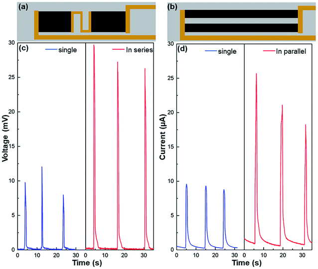
The generated electricity can be further scaled up through series and parallel connections of multiple graphene/TiO2 wave energy generators (Fig. 5 and S8†). As shown in Fig. 5c, an individual device (with a size of 1.5 × 2.5 cm2) induced around 10 mV peak voltage, but after connecting two identical films in series (Fig. 5c), the peak voltage was over 25 mV, increased by more than twice. Similarly, the short-circuit current increased from 9 μA for one individual device (with a size of 0.5 × 6.0 cm2) to about 20 μA after two devices are connected in parallel (Fig. 5d). The feasibility of series and parallel connection offers opportunities to scale up the wave energy harvesting. Certainly, it can be well expected that the electrical performance of our ocean wave energy generators can be further improved if they are combined with other mechanisms in literature, such as triboelectric, piezoelectric, thermoelectric, and solar evaporation-enhanced energy harvesting.26
Conclusions
In summary, we have developed a facile process to fabricate wave energy generators based on graphene/TiO2 nanoparticle composites. When cyclically inserted into and pulled out of simulated seawater, the devices could generate a voltage of up to 75 millivolts with a maximum power of nearly 1.8 μW. The devices exhibit good stability, with no evident performance degradation after 200 cycles. The output voltage increases linearly with the insertion velocity, insertion depth and the interval time between the cycles, which agreed well with the existing theory for wave potential, whereas it exhibits non-monotonous dependence on the salt concentration. Furthermore, by series and parallel connections of multiple devices, the output voltage and current are scaled accordingly. This research is expected to expedite the development of wave energy generators in practical applications.Conflicts of interest
There are no conflicts to declare.Acknowledgements
Han Xue and Jiantong Li acknowledge the financial support of the Olle Engkvist Byggmästare Foundation (grant number 2014/799), ÅForsk Foundation (grant number 17-352), the Formas Foundation (grant number 2016-00496), the Swedish Research Council (grant number 2019-04731), and China Scholarship Council (grant number 201906230359). We gratefully thank Dr Mika-Matti Laurila (Tampere University, Finland) for helping us set up the speed motor for energy harvesting tests.Notes and references
- R. Pelc and R. M. Fujita, Mar. Policy, 2002, 26, 471–479 CrossRef.
- Z. L. Wang, Nature, 2017, 542, 159–160 CrossRef CAS PubMed.
- J. Scruggs and P. Jacob, Science, 2009, 323, 1176–1178 CrossRef CAS PubMed.
- G. W. Boehlert and A. B. Gill, Oceanography, 2010, 23, 68–81 CrossRef.
- J. Yin, Z. Zhang, X. Li, J. Yu, J. Zhou, Y. Chen and W. Guo, Nat. Commun., 2014, 5, 1–6 Search PubMed.
- Q. Tang, Z. Zhou and Z. Chen, Nanoscale, 2013, 5, 4541–4583 RSC.
- J. P. G. Tarelho, M. P. Soares dos Santos, J. A. F. Ferreira, A. Ramos, S. Kopyl, S. O. Kim, S. Hong and A. Kholkin, Mater. Today, 2018, 21, 1019–1041 CrossRef CAS.
- Z. Zhang, X. Li, J. Yin, Y. Xu, W. Fei, M. Xue, Q. Wang, J. Zhou and W. Guo, Nat. Nanotechnol., 2018, 13, 1109–1119 CrossRef CAS PubMed.
- G. Shi, L. Chen, Y. Yang, D. Li, Z. Qian, S. Liang, L. Yan, L. H. Li, M. Wu and H. Fang, Nat. Chem., 2018, 10, 776–779 CrossRef CAS PubMed.
- M. Ye, Z. Zhang, Y. Zhao and L. Qu, Joule, 2018, 2, 245–268 CrossRef CAS.
- L. P. Block, Astrophys. Space Sci., 1978, 55, 59–83 CrossRef.
- D. C. Grahame, Chem. Rev., 1945, 41, 441–501 CrossRef PubMed.
- S. L. Carnie and D. Y. C. Chan, J. Chem. Phys., 1983, 78, 3348 CrossRef.
- J. Yin, X. Li, J. Yu, Z. Zhang, J. Zhou and W. Guo, Nat. Nanotechnol., 2014, 9, 378–383 CrossRef CAS PubMed.
- G. Liu, T. Chen, J. Xu and K. Wang, J. Mater. Chem. A, 2018, 6, 18357–18377 RSC.
- S. Yang, Y. Su, Y. Xu, Q. Wu, Y. Zhang, M. B. Raschke, M. Ren, Y. Chen, J. Wang, W. Guo, Y. Ron Shen and C. Tian, J. Am. Chem. Soc., 2018, 140, 13746–13752 CrossRef CAS PubMed.
- J. Tan, Y. Zhao, X. Yang, J. Duan, Y. Wang and Q. Tang, J. Mater. Chem. A, 2019, 7, 5373–5380 RSC.
- J. Tan, J. Duan, Y. Zhao, B. He and Q. Tang, Nano Energy, 2018, 48, 128–133 CrossRef CAS.
- Z. Zhai, H. Shen, J. Chen, X. Li and Y. Li, ACS Appl. Mater. Interfaces, 2020, 12, 2805–2815 CrossRef CAS PubMed.
- W. Fei, C. Shen, S. Zhang, H. Chen, L. Li and W. Guo, Nano Energy, 2019, 60, 656–660 CrossRef CAS.
- Z. Zhen, et al. , 2D Materials, 2019, 6, 045040 CrossRef CAS.
- G. Liu, et al. , J. Mater. Chem. A, 2018, 6, 18357–18377 RSC.
- S. Sollami Delekta, M. M. Laurila, M. Mantysalo and J. Li, Nanomicro Lett., 2020, 12, 40 Search PubMed.
- J. Li, S. Sollami Delekta, P. Zhang, S. Yang, M. R. Lohe, X. Zhuang, X. Feng and M. Östling, ACS Nano, 2017, 11, 8249–8256 CrossRef CAS PubMed.
- X. Li, C. Shen, Q. Wang, C. M. Luk, B. Li, J. Yin and S. P. Lau, Nano Energy, 2017, 32, 125–129 CrossRef CAS.
- G. Liu, T. Chen, J. Xu, G. Li and K. Wang, J. Mater. Chem. A, 2020, 8, 513–531 RSC.
Footnote |
| † Electronic supplementary information (ESI) available: Experimental materials and methods. See DOI: 10.1039/d1na00658d |
| This journal is © The Royal Society of Chemistry 2022 |


