 Open Access Article
A self-supported ultrathin plasmonic film for ultrafast optical switching†
Jinghui
Yang
ab,
Yulan
Fu
 a and
Xinping
Zhang
 *a
*a
aInstitute of Information Photonics Technology, Beijing University of Technology, Beijing, 100124, P. R. China. E-mail: zhangxinping@bjut.edu.cn
bModern Police Technology and Equipment Research Center, College of Police Equipment and Technology, China People's Police University, Langfang, 065000, P. R. China
First published on 4th January 2022
Abstract
Self-supporting gold nanowire (AuNW) gratings with a thickness of about 200 nm are produced by solution-processing and flexible-transfer techniques. Such an ultrathin structure is applied as an ultrafast optical switch that enables low-threshold optical modulation with a high signal contrast and a high signal-to-noise ratio. Transient energy-band modification in gold under excitation by femtosecond laser pulses is the main responsible mechanism. For a pump fluence of about 170 μJ cm−2, a modulation depth of about 10% is achieved for the optical switching signal. Self-supporting metallic plasmonic photonic thin films with a large area and flexible structures are important for applications in a large variety of circumstances and on different interfaces for optical signal processing, optical logic circuits, and optical communication systems.
1. Introduction
A variety of all-optical switches based on metallic plasmonic nanostructures have been proposed and investigated extensively for potential applications in optical communication, networking, optical computation, and optical logic circuits.1–5 Design of structures and devices with novel photophysical properties for low-threshold and low-energy-consumption applications has always been the focus of this research field.6–10 Our recent discoveries revealed that the band-structure modulation by the strong optical electric field of femtosecond laser pulses has been one of the most important photophysical properties for the optical switching effect.11–13 Such optical processes induce a red-shift of the threshold for interband transition in metallic photonic structures, so that optical extinction spectra by both interband absorption and localized surface plasmons are modulated strongly. Enhancement in interband absorption at shorter wavelengths and reduction in plasmonic optical extinction at longer wavelengths than the threshold point for interband transitions will thus be observed. Furthermore, most of the reported plasmonic optical switches have been metallic photonic structures on solid substrates, implying rigid and large-scale devices.14–21 Thus, transfer and miniaturization of this group of devices are other aspects for the development of plasmonic optical switching techniques. Recently, we reported a fiber-tip-integrated plasmonic optical switch for long-range optical signal transmission or remote signal processing, which enables miniaturization of the device and flexibilization of the signal-delivering system.22 In this work, we demonstrate flexibilization of the device for ultrafast optical switching and its integration potential on various surfaces or interfacial structures of different photonic systems, which greatly expands the application circumstances of such plasmonic devices. This is realized by a self-supported ultrathin grating of gold nanowires.2. Fabrication of self-supported thin-film (SSTF) AuNW gratings
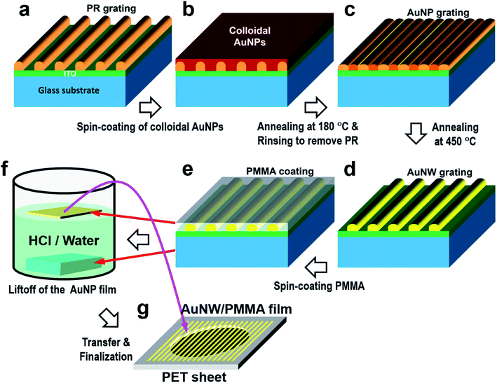
An ultrathin and flexible self-supported film of a gold nanowire grating was produced using combined techniques of interference lithography, solution-processing of colloidal gold nanoparticles, multistep annealing, and flexible transfer, as has been described in our previous publications.23,24 The whole procedure is described in detail in Fig. 1. As shown in Fig. 1(a), a photoresist (PR) grating is produced by interference lithography on a glass substrate that is coated with a 200 nm indium-tin-oxide (ITO) buffer layer. An ultraviolet (UV) laser at 360 nm and a positive photoresist, S1805, are employed in interference lithography. The produced PR grating has a period of about 450 nm and a modulation depth of more than 200 nm. Then, chemically synthesized colloidal gold nanoparticles suspended in xylene with a concentration of 100 mg ml−1 were spin-coated onto the PR grating at a speed of 2000 rpm for 30 s, as shown in Fig. 1(b).A two-stage annealing process is carried out to metallize the grating structures. In the first stage, the sample was heated to 180 °C for 2 minutes in order to sublimate the ligands covering the surface of the gold nanoparticles and to melt and confine colloidal gold nanoparticles into the grating grooves, as shown in Fig. 1(c). In the second stage, a high annealing temperature of 450 °C is used and the sample is annealed in a muffle furnace for about 20 min, which may not only melt the gold completely to produce continuous gold nanowires but also remove the photoresist completely, as shown in Fig. 1(d). Then, a thin layer of polymethyl methacrylate (PMMA) is spin-coated onto the top surface of the gold nanowire grating, which has a thickness of about 250 nm and is used to connect all of the gold nanowires, as shown in Fig. 1(e). In the final stage, the sample is immersed in hydrochloric acid (HCl) with a concentration of 20% for more than 30 min to etch the ITO buffer layer. Thus, the PMMA-connected gold nanowires are lifted from the glass substrate, as shown in Fig. 1(f), which is what we define as an ultrathin plasmonic film for optical switching applications.
To pick up the gold-nanowire grating, a sheet of polyethylene terephthalate (PET) is prepared in advance with a circular hole as large as 5 mm in diameter, which is used as a pick-up holder. After the gold nanowires are transferred onto the PET holder, they are rinsed in deionized water to remove the remaining HCl. Fig. 1(g) illustrates the finalized structure.
The top-view and cross-sectional images, respectively, in Fig. 2(a) and (b) show the scanning electron microscopy (SEM) characterization of the AuNWs embedded in the flexible PMMA film. Thin gold nanowires with a width smaller than 100 nm are distributed homogeneously with a period of 450 nm in an area of about 1 cm in diameter. As shown in Fig. 2(b), the PMMA thin film has a thickness of about 240 nm, which is identical to the thickness of the optical switching structure. The free-standing area of the gold nanowire grating has a diameter of 5 mm, which is defined by the circular hole in the PET holder. The three photographs in the inset of Fig. 2(c) not only show the large-area thin-film grating structures, but also demonstrate strong diffractions into different colors. These images were captured by a digital camera when the structures were illuminated by the flashlight produced by the camera itself. The bright diffraction pattern in Fig. 2(c) covering the spectral band from the blue to the red verifies the high quality and large-area homogeneity of the gold nanowire grating, where a white-light laser beam with a diameter of about 3 mm was sent to the thin-film structures and diffracted efficiently into a stable color pattern. A white screen was placed behind the sample to collect the diffracted light, so that the diffraction pattern can be recorded using a digital camera. After being transferred, the thin-film structure does not exhibit obvious wrinkles or defects. Furthermore, the thin-film structure remains stable on the PET holder, which constitutes the final configuration of the optical switch.
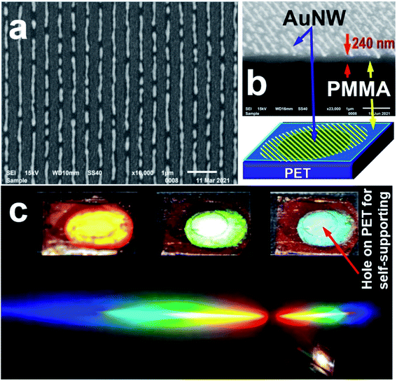 | ||
| Fig. 2 (a) SEM image of the AuNWs on an ITO glass substrate. (b) SEM image of the self-supporting AuNW film. (c) Diffraction patterns of the self-supporting AuNW film in the visible region. | ||
3. Plasmonic resonance modes in the self-supported AuNW-grating film
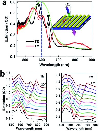
Fig. 3 shows the optical extinction spectroscopic response of the thin-film AuNW grating. The inset of Fig. 3(a) depicts the geometry for the measurement. A tungsten halogen lamp supplies the white-light source, which is incident at an angle of θ after being collimated and sent through a polarizer. The polarization perpendicular to the AuNWs is defined as the TM mode and that along the AuNWs as the TE mode. The optical extinction is defined by –log10[I(λ)/I0(λ)], where I(λ) and I0(λ) denote the transmission spectrum through the self-supported thin-film structure with and without the AuNW grating structures, respectively. The structure was rotated about an axis parallel to the AuNWs in the measurement of the angle-resolved tuning properties.The optical extinction spectroscopic response of the self-supporting AuNW film was measured in a spectral range from 450 nm to 900 nm. Fig. 3(a) shows the measurement results for normal incidence. As shown in Fig. 3(a), for TM polarization, Fano coupling of the localized surface plasmon in the AuNWs with the Rayleigh anomaly and with the waveguide resonance mode can be observed, which are highlighted by the red circle (590 nm) and red triangle (647 nm), respectively. In contrast, these two features change from dips in the optical extinction spectrum to peaks for TE polarization, as highlighted by the black circle (578 nm) and the black triangle (638 nm), implying no Fano coupling between the LSP and the Rayleigh/waveguide resonance modes. The waveguide is supplied by the PMMA thin film. It needs to be noted that the optical switching effect is mainly based on the optical modulation on the LSP of the gold nanowires, and therefore, we care more about the spectral location of the LSP. According to the red spectrum in Fig. 3(a), we can estimate a LSP spectrum extending from 500 to about 650 nm, which is centered in the range between 550 and 600 nm, as indicated by the dashed green curve.
Fig. 3(b) demonstrates the angle-resolved tuning properties of the optical extinction spectrum for TE and TM polarizations, where the angle of incidence is increased from 0 to 20°. For TE polarization, three major spectral features can be observed, which appear as optical extinction peaks and shift upon changing the angle of incidence. The spectrum peaking at 638 nm splits into two peaks that shift in opposite directions. This is obviously a waveguide mode excited by the AuNW grating in the PMMA film. The other feature that peaked at 578 nm can be explained as the Rayleigh anomaly and evaluated by λR = neffΛ, where λR = 578 nm is the resonance wavelength, Λ = 450 nm is the grating period, and neff is the effective refractive index with the AuNWs half-buried in PMMA. These three features can find their correspondence in the measurement results for TM polarization. However, spectral dips, instead of peaks, are observed for these spectral features for TM polarization, where their Fano coupling with the LSP of the AuNWs is the responsible mechanism. The spectral dip at 647 nm splits into two branches and evolves in opposite directions. The right one becomes peaks at wavelengths longer than 700 nm, because the LSP resonance spectrum does not cover the waveguide mode anymore. This mechanism also applies to the Rayleigh anomaly centered at 590 nm at normal incidence. It needs to be noted that under strong optical excitation by femtosecond pulses, we did not observe any obvious modification in the waveguide resonance mode, since PMMA is found to have a weak nonlinear optical response. On this basis, the waveguide resonance mode and its Fano coupling with the LSP did not contribute much to the optical switching effect, as will be demonstrated in Section 4.
4. Low-threshold ultrafast optical switch
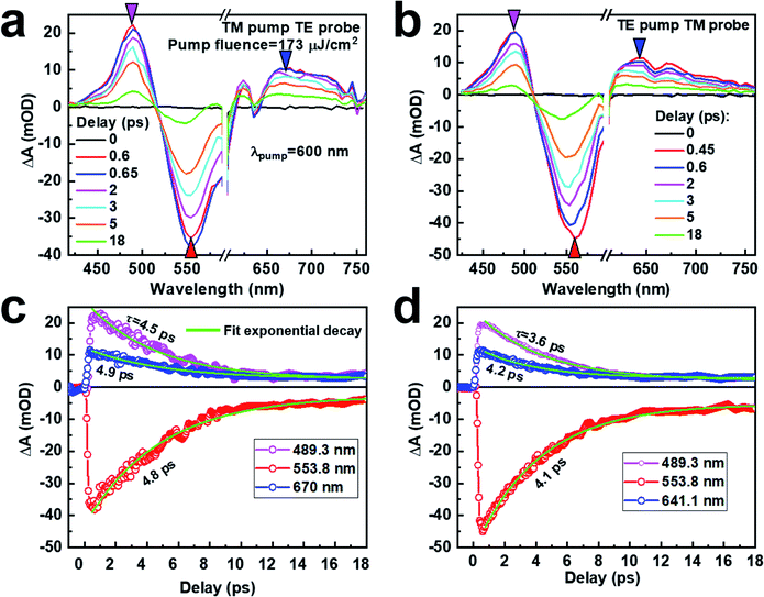
In the investigation of the ultrafast optical switching effects, a femtosecond pump–probe system was employed to measure the transient absorption (TA) spectroscopic response of the self-supporting AuNW grating film. The pump laser pulses are supplied by an optical parametric amplifier and are centered at 600 nm, having a pulse duration of about 150 fs and a repetition rate of 1 kHz. A small portion of the 800 nm pulses directly output from the Ti:sapphire amplifier is sent to a quartz cell containing heavy water with a thickness of 3 mm to produce supercontinuum pulses extending from 340 to 1200 nm, which are used as the probe pulses.25 The transient absorption spectrum defined as ΔA(λ) is measured as a function of the time delay (Δτ) between the pump and probe pulses. The pump pulses centered at 600 nm induce a rough peak excitation of the LSP, as shown by the dashed blue line in Fig. 3(a). The pump and probe laser beams have diameters of about 1 mm and 600 μm, respectively, and they have a separation angle of about 7 degrees. To avoid the interference effect between the pump and probe pulses,26 we use orthogonal polarizations for the pump and probe pulses, i.e. the TE-pump/TM-probe or TM-pump/TE-probe scheme. For comparison, we also include the measurement results for the TE-pump/TE-probe and TM-pump/TM-probe schemes in Fig. S1 in the ESI.† In Fig. S1(a) and (b),† for the TE-pump/TE-probe and TM-pump/TM-probe schemes, respectively, oscillation in the TA dynamics can be observed for probing at 588.8 and 612.1 nm within the first 500 fs, which clearly results from the interference effect. However, for other probing wavelengths, we can observe excellent optical switching signals by the TA dynamics, as shown in Fig. S1(c) and (d)† for the TE-pump/TE-probe and TM-pump/TM-probe schemes, respectively.Fig. 4(a) and (b) show the TA spectra at different delays for the TM-pump/TE-probe and TE-pump/TM-probe schemes for normal incidence of the probe beam. A pump fluence of 173 μJ cm−2 was used for all of the measurements in Fig. 4. In Fig. 4(a), the TA spectra at Δτ = 0, 0.6, 0.65, 2, 3, 5, and 18 ps are included for the spectral range from 418 to 760 nm. Strong TA spectral features centered at about 489.3, 553.8, and 670 nm are observed, where the signal at 553.8 nm is a dip in the TA spectrum with negative transient absorption. Strong optical excitation by femtosecond laser pulses induces a redshift of the threshold for interband transitions,11,27–31 so that the interband absorption becomes enhanced in the spectral band with shorter wavelengths than the threshold, corresponding to the feature at 489.3 nm (magenta triangle). Meanwhile, the plasmonic band is pushed to the red, producing a left-negative and right-positive TA spectrum, as highlighted by the red and blue triangles. It needs to be noted that this effect is a generally existing mechanism for metallic nanostructures and is thus applicable to both TE and TM polarizations. However, this mechanism is more sensitive and obviously observed around the threshold point due to the steep falling and rising band edges, which explains the strongest TA signals at 489.3 and 553.8 nm. In contrast, the transient spectroscopic response is weak at the falling edge of the plasmonic band, which generally varies slowly with increasing wavelength and can be observed for both TE and TM polarizations in Fig. 4(a) and (b), respectively.
Fig. 4(b) shows the TA spectra for the TE pump and TM probe at delays of 0, 0.45, 0.6, 2, 3, 5, and 18 ps. Again, three prominent spectral features can be observed to peak at 489.3, 553.8, and 641.1 nm. The largest negative signal at 553.8 nm is observed at Δτ = 0.45 ps, which is 200 fs earlier than that for the TM-pump/TE-probe scheme, implying a faster rising speed of the signal. The dip signal at 553.9 nm is enhanced considerably, which is increased from 38 mOD to 45 mOD, corresponding to about 18% enhancement. This verifies the more efficient excitation of the LSP in the AuNWs for TM than for TE polarization. However, the TM pump is actually more efficient at excitation. Therefore, the efficiency is not an optimized value for the TE-pump/TM-probe scheme. In practice, to avoid the interference between the pump and probe pulses, we had to avoid the TM-pump and TM-probe scheme. Therefore, we have to compromise between TM excitation and TM probing to achieve a better efficiency.
The most obvious difference between the TA spectra in Fig. 4(a) and (b) is the spectral dip at about 636 nm in Fig. 4(a), which becomes weakened and is red-shifted to 658 nm in Fig. 4(b). This feature is the transient response of the waveguide resonance mode for TE polarization and its Fano coupling with localized surface plasmons for TM polarization, which is stronger and sharper for TE than for TM polarization, as defined in Fig. 3(a) by the black and red triangles. However, neither of them introduced strong optical modulation or made an important contribution to the optical switching signals. Therefore, we do not focus our investigations on these features.
Fig. 4 (c) and (d) show the TA dynamics for the TM-pump/TE-probe and TE-pump/TM-probe schemes, respectively. In Fig. 4(c), TA dynamics at 489.3, 553.9, and 670 nm are plotted and fitted using first-order exponential decay. Lifetimes of 4.5, 4.8, and 4.9 ps are measured for these optical switching signals at 489.3, 553.9, and 670 nm, respectively. Apparently, the signals at 489.3 and 553.9 nm have better contrast than that at 670 nm. This means that the response of bandstructure modulation is more sensitive than that of the plasmon to the optical excitation, leading to higher optical switching efficiency and relatively higher speed.
It is known that for optical excitation there are generally three stages for plasmon-electronic dynamics: a pure electronic process (<500 fs), electron–phonon interaction process (0.5–5 ps), and phonon–phonon interaction process (>5 ps, lasts for more than 100 ps).32 In our fittings to the experimental data, we use the tail of the dynamic curve starting from 0.5 ps and stopping at 18 ps. Therefore, the dominant process is the electron–phonon interaction, where the long slow-variation tail for phonon–phonon interactions can be taken as the baseline of the dynamics. It is thus reasonable to fit the tail of the dynamics using a first-order exponential decay function. Although the electron–phonon interaction is the dominant process for nearly all of the measured dynamics, different electronic excitation processes are involved at different wavelengths. At wavelengths shorter than 520 nm, interband electronic excitation is the dominant process, and for longer wavelengths the plasmonic electronic oscillation/scattering and intraband excitation play more important roles. These factors determine different decay lifetimes at different wavelengths.
Compared with the TM-pump/TE-probe scheme, optical switching signals exhibit a larger amplitude and faster speed for the TE-pump/TM-probe, as shown in Fig. 4(b). In addition to the enhancement of the modulation depth from 38 to 45 mOD, there is an increase of more than 700 fs in the switching speed. The decay lifetime is reduced from 4.8 ps to 4.1 ps at 553.8 nm. As mentioned above, TM-polarized light excites electronic oscillations mainly with plasmonic resonance, while TE-polarized excitation corresponds to more bandstructure modulation. This applies to both the pump and probe pulses. The balance between the pump and probe schemes determines the final performance of the optical switching signal. Now that the bandstructure modulation is more sensitive to optical excitation than the LSP, strong TE-polarized excitation with weak TM probing produces stronger and faster optical switching signals. Moreover, compared with the TE-pump, the TM-pump induces additional strong localized surface plasmons, so that the electronic processes are delayed by further oscillation dynamics, which is in the order of a few hundreds of femtoseconds. This agrees well with the lifetime difference between the two pump–probe schemes.
To verify that our experiments are still within the linear response range of the plasmonic nanostructures, we measured the pump fluence dependence of the optical switching signals. Considering that the pump fluence at 800 nm is more than one order higher than that at 600 nm, the measurement results for 800 nm pumping are more reasonable to justify the damage threshold of the plasmonic structure. Therefore, we show in Fig. 5(a) the pump fluence dependence of the TA dynamics (optical switching signal) at 533.5 nm for the TE-pump/TM-probe scheme. When the pump fluence is increased from 1.2 to 4.6 mJ cm−2, the absolute amplitude of the negative optical switching signal increases from |ΔA| = 21.9 to 47.3 mOD. If we plot the variation of the signal amplitude as a function of pump fluence, as shown by the solid circles in Fig. 5(b), we may find that the variation has a precise linear relationship for a pump fluence below 2.5 mJ cm−2, according to the linear fitting results (dashed red line), implying stable optical switching operation. However, as the pump fluence is increased to 4.6 mJ cm−2, the linear dependence cannot be maintained further, implying saturation of the process or damage to the structures. Meanwhile, we have also fitted the tails of the TA dynamics in Fig. 5(a) using the function of exponential decay and consequently determined the lifetimes of these dynamic processes, which are 2.16, 2.61, 3.77, and 4.33 ps for the pump fluences of 1.2, 1.7, 2.5, and 4.6 mJ cm−2, respectively. This dependence is plotted in Fig. 5(b) by empty squares. Again, a roughly linear relationship can be justified for the pump fluence below 2.5 mJ cm−2, as demonstrated by the dashed blue line. For higher pump fluence, the optical switching signal tends to decay faster, again implying saturation of the signal or damage to the structures. These measurement results with reasonable analysis define an upper limit for the excitation strength of this optical switch. Using the dashed red line in Fig. 5(b), we estimate such a limit for pump fluence to be about 3.2 mJ cm−2, as indicated by the red circle.
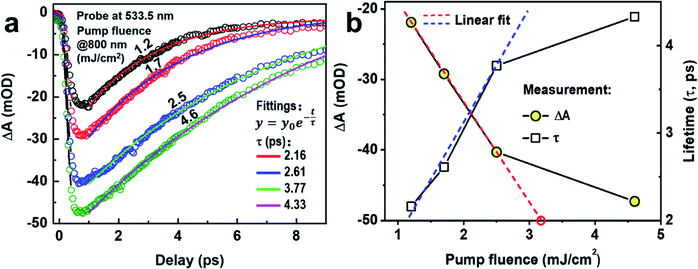 | ||
| Fig. 5 (a) TA dynamics as optical switching signals at different pump fluences for 800 nm pumping and 533.5 nm probing. (b) Optical signal amplitude and decay lifetime as a function of pump fluence. | ||
Although the excitation strength at 600 nm is much weaker than that at 800 nm, it is still necessary to make a comparison between the experimental results. The plot of the optical switching signal as TM-polarized TA dynamics at 553.8 nm for TM pumping at 600 nm with the pump fluence increased from 10 to 33, 72, 102, and 180 μJ cm−2 is shown in Fig. S2(a).† Since the pump fluence at 600 nm is much lower than that at 800 nm, we basically observe a linear dependence of the optical switching signal on the pump fluence, as shown by the plot in Fig. S2(b).†
5. On- versus off-resonance pumped optical switching
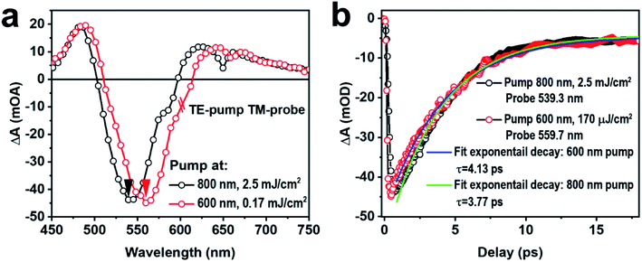
To understand the low-threshold performance of the ultrathin optical switch, we compare the optical switching performance for excitation pulses at 600 and 800 nm, which are within and outside the resonance spectrum of the LSP. Fig. 6(a) and (b) show the TA spectra (at maximum amplitude) and dynamics (at peak wavelength), respectively, where TE-pumping at 600 and 800 nm pulses with different pump fluences has been employed for TM-probing. Although there is a redshift of the TA spectrum for pumping at 600 nm with respect to that at 800 nm, where the dip maximum shifts from 539.3 to 559.7 nm, these two spectra are quite similar in their shapes and amplitudes, implying the involvement of quite similar photophysics. However, a pump fluence of 2.5 mJ cm−2 is employed for 800 nm pumping and 170 μJ cm−2 for 600 nm pumping, implying more than one order reduction (a factor of 14.7) in the threshold or more than one order enhancement in the efficiency of the optical switch. Moreover, for 800 nm pumping, due to the off-resonance excitation with more than one-order higher pump fluence, the thermal effect induced electron–photon and phonon–phonon scattering processes, as well as the consequent lattice-expansion effect, are much stronger than those for 600 nm pumping. All of these effects favor a larger red-shift of the surface plasmons for 800 nm pumping. However, it is understandable that such a thermal-effect-induced red-shift is much less spectrally selective than the on-resonance excitation at 600 nm, and therefore, it applies to nearly the whole spectrum.Fig. 6(b) shows the comparison between the TA dynamics measured at 539.3 nm for 800 nm pumping and 559.7 nm for 600 nm pumping, with the corresponding spectral position highlighted by the black and red triangles in Fig. 6(a), respectively. These two dynamic curves have nearly equal amplitudes, although they are measured at very different pump fluences, confirming again the much-enhanced working efficiency. According to Fig. 3(b), 600 nm is within the resonance spectrum of the LSP of the AuNWs, while 800 nm is far outside the resonance spectrum. Thus, the much-enhanced efficiency can be attributed to the on-resonance excitation of the LSP.
If we evaluate the efficiency of an ultrafast optical switch by the ratio between the signal amplitude and the pump fluence, we obtain an efficiency of 45 mOD/170 μJ cm−2 = 264.7 mOD mJ−1 cm2 for our ultrafast optical switch, which is much higher than the previously reported values. An optical modulation depth of 24% was reported for a photorefractive VO2/Au hybrid structure using a pump fluence of 15 mJ cm−2, which can be converted to an efficiency of 8 mOD mJ−1 cm2.33 A transient optical modulation of 15% was achieved in a self-organized metasurface of gold nanowires grown on silica for a pump fluence of 10 mJ cm−2, corresponding to an efficiency of about 7 mOD mJ−1 cm2.34 Our enhancement is even much higher when compared with the results in ref. 35 and 36. All of these comparisons justify an apparently much lower threshold and much higher efficiency of our ultrafast plasmonic optical switch here.
Furthermore, fittings to the dynamic curves using the first-order exponential decay function reveal that pumping at 800 nm results in faster dynamics than at 600 nm. Pumping at 800 nm produces optical switching signals with a speed of about 3.77 ps. However, upon pumping at 600 nm, we achieve an optical switching speed of about 4.13 ps, which is about 360 fs slower. Therefore, on-resonance pumping leads to considerably enhanced optical switching efficiency and signal amplitude; however, the speed of the signal is slightly reduced.
6. Conclusions
An ultrafast optical switch is achieved using an ultrathin AuNW grating based on a self-supporting scheme. A modulation depth of about 45 mOD (∼10%) for the transmission of visible pulses is obtained using a pump fluence of only 170 μJ cm−2 for 150 fs excitation pulses at 600 nm, corresponding to an efficiency of more than 260 mOD mJ−1 cm2. Transient modulation of the bandstructure of gold with high sensitivity by optical excitation is the main responsible mechanism. On-resonance excitation of the LSP of the AuNWs is responsible for the enhancement of the optical switching efficiency by a factor larger than 14.7. Such a self-supporting thin-film optical switch not only enables flexibly integrable plasmonic optical switching devices, but also makes it possible to transfer such structures onto various solid surfaces of other devices or systems. This is significant for greatly expanding the application circumstances and conditions of the plasmonic optical switch in optical signal processing, optical communication, and optical logic circuit systems.Conflicts of interest
There are no conflicts of interest to declare.Acknowledgements
The authors acknowledge the National Natural Science Foundation of China (61735002 and 12074020) and Beijing Municipal Education Commission (KZ202010005002) for their support.References
- I. Kriegel, C. Urso, D. Viola, L. D. Trizio, F. Scotognella, G. Cerullo and L. Manna, Ultrafast photodoping and plasmon dynamics in luorine–indium codoped cadmium oxide nanocrystals for all-optical signal manipulation at optical communication wavelengths, J. Phys. Chem. Lett., 2016, 7, 3873–3881 CrossRef CAS PubMed.
- Z. J. Zhang, J. B. Yang, X. He, Y. X. Han, J. J. Zhang, J. Huang, D. B. Chen and S. Y. Xu, All-optical multi-channel switching at telecommunication wavelengths based on tunable plasmon-induced transparency, Opt. Commun., 2018, 425, 196–203 CrossRef CAS.
- B. I. Afinogenov, V. O. Bessonov, I. V. Soboleva and A. A. Fedyanin, Ultrafast all-optical light control with Tamm plasmons in photonic nanostructures, ACS Photonics, 2019, 6, 844–850 CrossRef CAS.
- T. Hira, T. Homma, T. Uchiyama, K. Kuwamura, Y. Kihara and T. Saiki, All-optical switching of localized surface plasmon resonance in single gold nanosandwich using GeSbTe film as an active medium, Appl. Phys. Lett., 2015, 106, 031105 CrossRef.
- Z. Chai, Y. Zhu, X. Y. Hu, X. Y. Yang, Z. B. Gong, F. F. Wang, H. Yang and Q. H. Gong, On chip optical switch based on plasmon–photon hybrid nanostructure coated multicomponeonent nanocomposite, Adv. Opt. Mater., 2016, 4, 1159–1166 CrossRef CAS.
- P. Vasa, W. Wang, R. Pomraenke, M. Maiuri, C. Manzoni, G. Cerullo and C. Lienau, Optical Stark effects in J-aggregate–metal hybrid nanostructures exhibiting a strong exciton–surface-plasmon-polariton interaction, Phys. Rev. Lett., 2015, 114, 036802–036806 CrossRef CAS PubMed.
- D. S. Kim, S. C. Hohng, V. Malyarchuk, Y. C. Yoon, Y. H. Ahn, K. J. Yee, J. W. Park, J. Kim, Q. H. Park and C. Lienau, Microscopic origin of surface-plasmon radiation in plasmonic band-gap nanostructures, Phys. Rev. Lett., 2003, 91(4), 143901–143904 CrossRef CAS PubMed.
- A. Kumar, Y. Kumar Srivastava, M. Manjappa and R. Singh, Color-sensitive ultrafast optical modulation and switching of terahertz plasmonic devices, Adv. Opt. Mater., 2018, 6, 1800030–1800036 CrossRef.
- Y. H. Lin and X. P. Zhang, Ultrafast multipolar plasmon for unidirectional optical switching in a hemisphere-nanoshell array, Adv. Opt. Mater., 2017, 5, 1601088 CrossRef.
- Y. Wang and X. P. Zhang, Ultrafast optical switching based on mutually enhanced resonance modes in gold nanowire gratings, Nanoscale, 2018, 10, 16193–16222 RSC.
- X. P. Zhang, M. Wang, F. W. Tang, H. Z. Zhang, Y. L. Fu, D. Liu and X. Y. Song, Transient electronic depletion and lattice expansion induced ultrafast bandedge plasmons, Adv. Sci., 2020, 7, 1902408 CrossRef CAS PubMed.
- X. P. Zhang, H. B. Wang, M. Wang, Y. H. Lin and X. Y. Song, Ultrafast particle-plasmon enhancement by energy-band modification in nanostructured tungsten carbide, Opt. Express, 2016, 24, 22730–22740 CrossRef CAS PubMed.
- X. P. Zhang, Plasmon extinguishment by bandedge shift identified as a second-order spectroscopic differentiation, Nanophotonics, 2021, 10, 1329–1335 CrossRef.
- K. D. Wang, L. Chen, H. J. Zhang and J. Chen, Controlling surface plasmon polaritons at femtosecond timescales on an aluminum-coated grating, Appl. Phys. Lett., 2017, 110, 021105–21114 CrossRef.
- C. P. McPolin, N. Olivier, J. S. Bouillard, D. O'Connor, A. V. Krasavin, W. Dickson, G. A. Wurtz and A. V. Zayats, Universal switching of plasmonic signals using optical resonator modes, Light: Sci. Appl., 2017, 6, e16237–e16238 CrossRef CAS PubMed.
- N. Kumar, A. Rúa, J. Aldama, K. Echeverria, F. E. Fernández and S. Lysenko, Photoinduced surface plasmon switching at VO2/Au interface, Opt. Express, 2018, 26(11), 11068–11077 CrossRef CAS PubMed.
- Z. Chai, X. Y. Hu, F. F. Wang, X. X. Niu, J. Y. Xie and Q. H. Gong, Ultrafast all-optical switching, Adv. Opt. Mater., 2017, 5, 1600665–1600721 CrossRef.
- S. W. Sim, H. Jang, N. Koirala, M. Brahlek, J. Moon, J. H. Sung, J. Park, S. Cha, S. Oh, M. H. Jo, J. H. Ahn and H. Choi, Ultrahigh modulation depth exceeding 2,400% in optically controlled topological surface plasmons, Nat. Commun., 2015, 6, 9814–9817 Search PubMed.
- C. C. Lu, X. Y. Hu, K. B. Shi, Q. Hu, R. Zhu, H. Yang and Q. H. Gong, An actively ultrafast tunable giant slow-light effect in ultrathin nonlinear metasurfaces, Light: Sci. Appl., 2015, 4, e302–e309 CrossRef CAS.
- A. Thomas, P. Savaliya, K. Kumar, A. Ninawe and A. Dhawan, Au nanowire-VO2 spacer-Au film based optical switches, J. Opt. Soc. Am. B, 2018, 35, 1687–1697 CrossRef CAS.
- Y. H. Lin, X. P. Zhang, X. H. Fang and S. Y. Liang, A cross-stacked plasmonic nanowire network for high-contrast femtosecond optical switching, Nanoscale, 2015, 8, 1421–1429 RSC.
- J. H. Yang and X. P. Zhang, Optical fiber delivered ultrafast plasmonic optical switch, Adv. Sci., 2021, 8, 2100280 CrossRef CAS PubMed.
- X. P. Zhang, J. Zhang, H. M. Liu, X. Q. Su and L. Wang, Soft plasmons with stretchable spectroscopic response based on thermally patterned gold nanoparticles, Sci. Rep., 2014, 4, 4182 CrossRef PubMed.
- Y. Wang, F. F. Liu and X. P. Zhang, Flexible transfer of plasmonic photonic structures onto fiber tips for sensor applications in liquids, Nanoscale, 2018, 10, 16193–16200 RSC.
- X. P. Zhang, F. W. Tang, M. Wang, W. B. Zhan, H. X. Hu, Y. R. Li, R. H. Friend and X. Y. Song, Femtosecond visualization of oxygen vacancies in metal oxides, Sci. Adv., 2020, 6, eaax9427 CrossRef CAS PubMed.
- X. P. Zhang, J. F. He, Y. M. Wang and F. F. Liu, Terahertz beat oscillation of plasmonic electrons interacting with femtosecond light pulses, Sci. Rep., 2016, 6, 18902–18908 CrossRef CAS PubMed.
- C.-K. Sun, F. Vallée, L. H. Acioli, L. H. Acioli, E. P. Ippen and J. G. Fujimoto, Femtosecond-tunable measurement of electron thermalization in gold, Phys. Rev. B: Condens. Matter Mater. Phys., 1994, 50, 15337–15348 CrossRef CAS PubMed.
- N. D. Fatti, C. Voisin, M. Achermann, S. Tzortzakis, D. Christofilos and F. Vallée, Nonequilibrium electron dynamics in noble metals, Phys. Rev. B: Condens. Matter Mater. Phys., 2000, 61, 16956–16966 CrossRef.
- C. Voisin, D. Christofilos, P. A. Loukakos, N. D. Fatti, F. Vallée, J. Lermé, M. Gaudry, E. Cottancin, M. Pellarin and M. Broyer, Ultrafast electron-electron scattering and energy exchanges in noble-metal nanoparticles, Phys. Rev. B: Condens. Matter Mater. Phys., 2004, 69, 195416–195513 CrossRef.
- P. Guo, R. D. Schaller, J. B. Ketterson and R. P. H. Chang, Ultrafast switching of tunable infrared plasmons in indium tin oxide nanorod arrays with large absolute amplitude, Nat. Photonics, 2016, 14, 1–8 Search PubMed.
- C. Voisin, N. D. Fatti, D. Christofilos and F. Vallee, Ultrafast electron dynamics and optical nonlinearities in metal nanoparticles, J. Phys. Chem. B, 2001, 105, 2264–2280 CrossRef CAS.
- J.-Y. Bigot, V. Halté, J.-C. Merle and A. Daunois, Electron dynamics in metallic nanoparticles, Chem. Phys., 2000, 251, 181–203 CrossRef CAS.
- N. Kumar, A. Rúa, J. Aldama, K. Echeverria, F. E. Fernández and S. Lysenko, Photoinduced surface plasmon switching at VO2/Au interface, Opt. Express, 2018, 26, 11068–11077 CrossRef CAS PubMed.
- G. Della Valle, D. Polli, P. Biagioni, C. Martella, M. C. Giordano, M. Finazzi, S. Longhi, L. Duò, G. Cerullo and F. Buatier de Mongeot, Self-organized plasmonic metasurfaces for all-optical modulation, Phys. Rev. B: Condens. Matter Mater. Phys., 2015, 91, 235440 CrossRef.
- G. Grinblat, R. Berté, M. P. Nielsen, Y. Li, R. F. Oulton and S. A. Maier, Sub-20 fs all-optical switching in a single Au-clad Si nanodisk, Nano Lett., 2018, 18, 7896–7900 CrossRef CAS PubMed.
- G. D. Valle, D. Polli, P. Biagioni, C. Martella, M. C. Giordano, M. Finazzi, S. Longhi, L. Duò, G. Cerullo and F. Buatier de Mongeot, Self-organized plasmonic metasurfaces for all-optical modulation, Phys. Rev. B: Condens. Matter Mater. Phys., 2015, 91, 235440 CrossRef.
Footnote |
| † Electronic supplementary information (ESI) available. See DOI: 10.1039/d1na00761k |
| This journal is © The Royal Society of Chemistry 2022 |

