 Open Access Article
Simple one pot synthesis of luminescent europium doped yttrium oxide Y2O3:Eu nanodiscs for phosphor converted warm white LEDs
Julian
Petry
ab,
Rajesh
Komban
 a,
Christoph
Gimmler
a and
Horst
Weller
ab
aFraunhofer-CAN, Grindelallee 117, 20146 Hamburg, Germany
bUniversity of Hamburg, Grindelallee 117, 20146 Hamburg, Germany
First published on 12th January 2022
Abstract
Yttrium oxide (Y2O3) is considered as one of the best host lattices for europium (Eu3+) based red emitting phosphors because of its unit cell and good photo-saturation properties. As a bulk material, it reaches nearly 100% quantum yield. However, providing high quality nanosized materials for the LED industry is still a challenge and not easily accomplished. Within this publication, a simple one pot, non-hydrolytic, solvent-based synthesis method for producing uniform and monodisperse red-emitting europium doped yttrium oxide (Y2O3:Eu) nanoparticles is provided. The synthesis is the cheapest and fastest reported yet, yields up to 80%, and offers good scalability, and the diameter of the produced nanodiscs is tunable from 7 nm to 30 nm. The dispersed nanomaterial shows bright red emission (607 nm) under UV excitation (273 nm) and a higher quantum yield (>30%) compared to other nanosized Y2O3:Eu materials. In order to shift the excitation wavelength towards the visible region we added Tb3+ as the sensitizer. Thereby, it was also possible to tune the emission colour towards orange/yellow. Further, a distorted anisotropic cubic Y2O3 phase is confirmed by XRD analysis, resulting in a distinct change in the intensities of red emission transitions. A calcination step transforms it into a highly crystalline cubic phase, known from the bulk material, and exhibiting a typical emission spectrum.
1. Introduction
Promising physical and chemical properties have made nanosized europium doped yttrium oxide (Y2O3:Eu) a widely studied nanomaterial over the last few years.1–6 Due to its stable, narrow and efficient red emission, it became an interesting material for optoelectronics, e.g. as phosphors7 in LEDs or as an emitter material in displays.8 With its low toxicity, Y2O3:Eu is a promising material system for use in nanobiotechnology and life sciences and does not fall under the ROHS directive.3For the next generation of phosphor converted warm white light emitting diodes (pc-WLEDs), nanosized materials9,10 play an important role. Lower energy consumption, environmental friendliness and high quality warm white light are the challenges of current LED development.9,11,12 A commercial WLED is usually fabricated as a blue emitting InGaN chip combined with a yellow emitting YAG:Ce3+ phosphor. Applying an additional red component such as Y2O3:Eu allows the LED to emit a warmer light with excellent colour quality.12–14 Weak absorption in the blue spectral range has prevented the use of Eu3+ phosphors for applications based on blue LEDs until now.10 Therefore, new approaches for Eu3+ sensitization were investigated. Via inter-particle Förster resonance energy transfer (IFRET) sensitization between lanthanide-doped nanoparticles was shown recently.10 Using this technique the use of different host materials for various sensitizer ions becomes available which also prevents metal-to-metal charge transfer quenching. Accordingly high quality, spherical and uniform nanomaterials are required which allow necessary sensitizer–emitter distances of 0.5–1.5 nm.15,16 The good photo-saturation behaviour and the possibility of high doping levels, i.e. high Eu3+ ion density per unit cell, make Y2O3 a superior host lattice when compared to the well-established nanosized vanadate or phosphate particles. Taking this as a motivation, we established a synthesis route with Eu3+ and Tb3+ doping at the same time to further study the influence of both ions within one nanoparticle.
Depending on the synthesis method used, different crystal structures for yttrium oxide can be achieved. Most common synthesis procedures are flame spray pyrolysis,1,17 combustion,2,18,19 and precipitation/sol–gel followed by heating/sintering.8,20–24 Each of these routes yields cubic yttrium oxide. Additionally, methods yielding a monoclinic17,25,26 crystal structure, specifically by gas-phase condensation26 or laser deposition, are well known.27 Also, nonhydrolytic low temperature (<300 °C) procedures are described3,4,28 yielding materials having a low crystallinity and/or a distorted4 cubic crystal structure. Herein, rare earth salts mixed with organic solvents and a final heating process led to the formation of yttrium oxide. Applying different synthesis routes, many different shapes of Y2O3:Eu such as nanodiscs,4 nanoplates,28 and wire-like29 or flower-like30,31 structures are described. Each method has its own advantages and disadvantages. All manufacturing procedures which make use of a high temperature sintering step yield highly crystalline materials having a bright emission20,22,24,29 and are well suited for their use as phosphors. At the same time, sintering results in particulate matter too large to be well dispersed in any given solvent, limiting the applicability of the materials. At temperatures >600 °C all organic matter is burnt leading to clean oxidic surfaces making post-synthetic functionalization impossible. By contrast, a nonhydrolytic synthesis route yields well dispersible4 nanoparticles which are usable for biofunctionalization. At the same time, lower reaction temperatures (<300 °C) lead to poor crystallinity and consequently, less bright emission.20,22,24,29
In this article, we present an improved simple nonhydrolytic one-pot synthesis by far easier and faster than any of the reported procedures so far.3,4,28 Furthermore, the synthesis procedure is scalable and the size of the nanodiscs can be tuned from 10 nm to 30 nm. Both parameters play an important role in industrial manufacturing and applications. By mixing only four chemicals, we were able to obtain much better defined spherical nanoplatelets exhibiting a strong red emission under UV excitation. At the same time good dispersibility is provided by oleic acid/oleylamine ligands allowing for further surface modification and functionalization. To optimize the luminescence properties for phosphor applications, we established a post-synthetic heating procedure increasing the crystallinity and emission intensity but at the same time retaining the original nanosized form.
2. Experimental
2.1 Chemicals
Yttrium chloride hexahydrate (99.9%) and europium chloride hexahydrate (99.9%) were purchased from Treibacher, oleic acid (technical grade, 90%) and cyclohexane (99.5%) from Sigma Aldrich, and oleylamine (technical grade, 80–90%) from Acros Organics. All chemicals were used without further purification.2.2 Synthesis of Y2O3:Eu
For a typical synthesis (10% Eu doping concentration), 0.2 mmol europium chloride hexahydrate and 1.8 mmol yttrium chloride hexahydrate were dissolved in 20 mL oleic acid and heated to 80 °C under vacuum for approximately 1 hour. Then, 50 mL oleylamine was added and degassed under vacuum for 1 hour. Subsequently, the mixture was heated to 300 °C and stirred under a nitrogen atmosphere for one hour. After cooling down to room temperature the nanodiscs were precipitated with 50 mL ethanol and collected by centrifugation. The final product was redispersed in 10 mL cyclohexane. For annealing experiments the material was dried in a vacuum chamber for 2 hours and heated for 1 hour in air. Characterization results show a product yield of 80%.2.3 Characterization
Transmission electron microscopy (TEM) images were taken using a JEOL JEM-1011 operating at 100 kV. 1 μL of the obtained suspension was mixed with 5 mL cyclohexane and 3 μL of the dilute solution was dried on a copper grid. For X-ray diffractometry a PANalytical X'PERT Pro diffractometer with a Cu Kα X-ray source (0.154 nm) and Bragg–Brentano geometry was used. Here, 100 μL of the suspension was dried on a Si wafer. The PL spectra were collected on a Photon Technology Interactive (PTI) spectrometer. The excitation wavelength was 273 nm. Quantum yield measurements were performed using a Hamamatsu C9920-02G. The annealed samples were dispersed in ethanol and an aliquot of 100 μL was dried on a Si wafer for the XRD measurements. For TEM analysis, 3 μL was dried on a copper grid.3. Results and discussion
3.1 TEM and XRD analysis
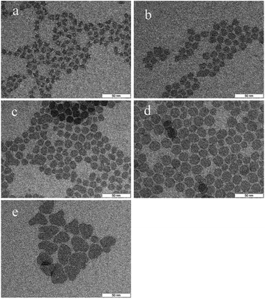
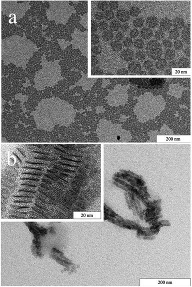
In Fig. 1, TEM images of the as-prepared nanomaterial are shown. Spherical nanoplatelets having an average diameter of 13.8 nm were obtained. These discs are well separated due to the presence of oleylamine/oleic acid as ligands. By varying the dispersant, the orientation and interaction of the discs can be controlled.28 In an organic solvent the hydrophobic ligands are well immersed and result in good dispersibility (Fig. 1a). When the solvent polarity increases, the orientation of the platelets changes and they align in stacks on the TEM grid as the hydrophobic ligands minimize the boundary surface energy (Fig. 1b).The time-dependent growth of the nanodiscs was studied and analysed by TEM (Fig. 2). By heating to 300 °C and immediate cooling, angular platelets having a size of approx. 7 nm were obtained. When the reaction time at 300 °C is increased, the platelets evolve into a disc-like shape and increase in diameter at the same time. During the first 45 minutes of growth, the standard size deviation for all samples analysed stays constant at around ± 1.5 nm indicating uniform growth of the particles by consumption of monomers. Afterwards, it increases to about ±4 nm and a second population of smaller platelets is observed for those samples. Hence, the platelet growth mechanism is now dominated by Ostwald ripening. At growth times beyond 120 minutes the platelets show a less uniform size and shape due to aggregation.
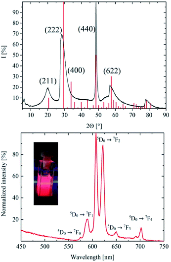
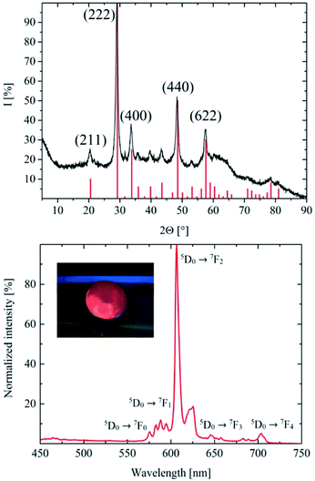
The XRD of the as-synthesized nanodiscs is shown in Fig. 3. Their peaks fit the reference PDF 1025-1011 from the crystal database rather well but at the same time exhibit a couple of differences. Due to the small size of the particles, there is distinct broadening of the peaks as is expected and well known for nanosized materials. In addition, a shift of the peak positions occurs which is attributed to the Eu (10%) doped host lattice. The absence of some of the reflections is expected due to the thin nano-disc morphology of the particles. In anisotropic-shaped particles, here ultrathin nano-discs, a limited number of planes are available, which directly reflect in diffraction experiments. The comparably low synthesis temperature of 300 °C for ceramic materials results in a rather poor crystallinity of the particles and a distorted unit cell of the cubic yttrium oxide nanomaterial. Furthermore, several differences in the peak width were found when compared to the library data. This difference is caused by the anisotropic shape of the ultrathin discs. To confirm the ultrathin disc shape of the nanomaterial the layer thicknesses were calculated by applying the Scherrer equation. Based on the peaks indicating the crystal planes at (211), (222), (440), and (622), thicknesses of 2.68 nm, 2.84 nm, 9.68 nm, and 1.72 nm were calculated, respectively. Accordingly, the crystalline layers along (440) are in plane (along the radius of the disc), whereas the others grow perpendicular to its axis. Due to its significant shoulder towards larger angles, the peak at 2Θ = 29° is assumed to be a superposition of the 2Θ = 29° and the 2Θ = 34° peak, another hint at the distorted crystal structure of the synthesized material.
3.2 Photoluminescence study
Yttrium oxide delivers the best photoluminescence intensity with a Eu3+ doping concentration of approximately 10%. The PL intensity changes as a function of the doping concentration are widely studied3,14,30–33 and will not be discussed in detail in this publication. Accordingly, all experiments were performed with a doping concentration of 10%. The PL spectrum of the obtained Y2O3:Eu 10% in cyclohexane (Fig. 3) shows a bright red emission at 607 nm and 622 nm caused by the 5D0 → 7F2 transition upon 273 nm host lattice excitation. Other peaks at 575 nm (5D0 → 7F0), 590 nm (5D0 → 7F1), 650 nm (5D0 → 7F3) and 702 nm are the results of the 5D0 → 7F4 transition. The spectroscopic terms and energy level structure of the Eu3+ emitter are published elsewhere.34,35 Compared to high temperature Y2O3:Eu30 the intensity ratio of the peaks in the PL spectrum of the platelets is clearly different. Similar emission spectra of low temperature Y2O3:Eu nanomaterials were previously published by Wang et al.4 and Das et al.3The differences in the spectral shape are caused by the anisotropic 2D crystal structure of the platelets described above. This structure results in a rather heterogenic environment for the Eu3+ emitter ions, whereas, in a highly crystalline, spherical Y2O3 material the doping ions uniformly replace yttrium in its lattice site, and the lower crystallinity and the 2D shape of the presented nanomaterial led to a less uniform surrounding for the doping ions. In the synthesized discs with a thickness of 2–3 nm, approximately 30% of the (440) layers are surface layers, resulting in a high fraction of surface Eu3+ ions. Surface atoms with a lower coordination number usually have lower symmetry and different electronic environments leading to a distinct emission spectra shape28,36.
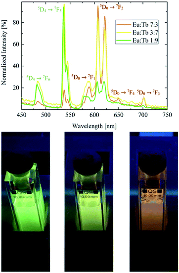
Photoluminescence spectra and photographs of the Y2O3:Eu,Tb co-doped nanodiscs are shown in Fig. 4. Increasing the Tb concentration results in a colour shift from red to green. The emission spectrum shows the characteristic Tb3+ lines at 480 nm (5D4 → 7F6) and 535 nm (5D4 → 7F5) whose intensities increase with the Tb3+ concentration. For this material system, excitation is possible at 393 nm (Eu3+ excitation), 485 nm (Tb3+ excitation) and <273 nm (host lattice excitation). Due to the energy transfer between Tb and Eu which was recently shown elsewhere10 all excitation wavelengths show the characteristic emission lines of Eu and Tb simultaneously as shown in Fig. 4.
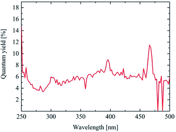
The photoluminescence quantum efficiency of the as-synthesized nanodiscs was measured for excitation wavelengths between 250 nm and 500 nm in steps of 2 nm. The emission at 607 nm was determined for each wavelength and the quantum yield calculated. The results are shown in Fig. 5. As reported7,8 the best quantum yield for Y2O3:Eu can be found around 250 nm excitation. The as-synthesized nanodiscs show a PL quantum efficiency up to 15% upon 250 nm excitation which is more than reported4,22 yet for a nanomaterial. Another maximum can be found at 393 nm (Eu3+ excitation) and 470 nm.
3.3 Annealing
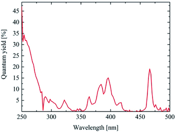
Heating experiments were conducted to investigate the effect of temperature and crystallinity on the emission spectra of the material. The X-ray diffraction of the annealed material is shown in Fig. 6. The XRD matches the reference data very well. The expected mean peaks are clearly visible despite the noise. The obtained X-ray diffraction points to a highly crystalline cubic yttrium oxide after annealing. The particle size was calculated using the Scherrer equation resulting in a diameter of 13 nm for every reflection of the XRD. By heating, the anisotropic shape of the platelets seems to be replaced by a more uniform three-dimensional geometric form matching the results of TEM analysis (Fig. 8). Fig. 6 also shows the PL emission spectrum of the corresponding annealed material and a photo of a powder sample exhibiting bright red emission under UV excitation is provided as the inset. The characteristic Y2O3:Eu emission spectrum was obtained where the 5D0 → 7F1 emission at 590 nm is now finely split into three lines. Moreover, the two most intense peaks at 607 nm and 622 nm caused by the 5D0 → 7F2 emission show the typical intensity ratio of highly crystalline (bulk) Y2O3:Eu.The photoluminescence quantum efficiency was also measured for the 600 °C annealed samples (Fig. 7). For a best comparison with the results of the as-synthesized material, the measurement parameters were kept the same. The PL quantum efficiency at 250 nm was much higher (>30%) for the heated samples compared to the as-synthesized material. Also, at 393 nm (18%) and 470 nm (20%) the photoluminescence of the materials is brighter due to the better crystallinity and the removed organic ligands.
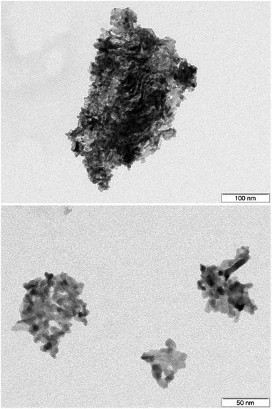 | ||
| Fig. 8 TEM images of the annealed samples (600 °C). Despite a tendency to agglomerate, individual nanoscale particles of spherical shape are clearly visible even after heating. | ||
For further investigation regarding the morphology of the annealed material, characterization by TEM was conducted (Fig. 8). Due to the removal of ligands, agglomeration of the synthesized discs was observed. Accordingly, it is not possible to determine the exact particle diameter but the nanosized structure clearly remains. The characteristic particle size is estimated to be approximately 15 nm.
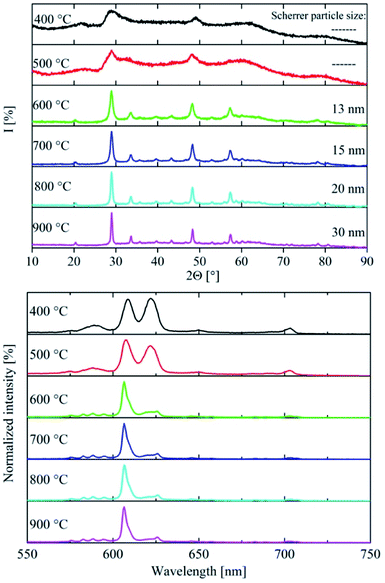
To better understand the annealing process and its influence on the optical properties of the material, we determined the transition temperature, where the change in optical properties starts to occur for the as-synthesized nano-discs. Therefore, the material was heated in steps of 100 °C from 400 °C to 900 °C and kept there for 1 hour. Each sample was investigated by XRD and the PL spectrum was recorded. Fig. 9 compares the results of these experiments with regard to the annealing temperature. No changes were observed for the material heated to 400 °C and 500 °C, respectively, neither in the XRD nor in the emission spectrum. Peak shapes and intensity ratios are the same for both as shown in Fig. 3. The sample annealed to 500 °C verifies the assumption of the superposition at 2Θ = 29° as the peak starts to split into two distinct lines. In contrast, the data obtained from the sample heated to 600 °C show significant differences as the shapes of the XRD and emission spectrum have changed. Consequently, a transition of the crystal structure happens between 500 °C and 600 °C with the observed changes described in detail above. No further changes in the emission spectrum were found when heating the sample material to 900 °C. Since the size of the particles increases with respect to temperature, peak narrowing in XRD is observed correspondingly. Applying the Scherrer equation, the respective particle sizes were calculated to be 13 nm (600 °C), 15 nm (700 °C), 20 nm (800 °C) and 30 nm for 900 °C. Similar calculations for the samples heated to only 400 °C and 500 °C were not possible, because collected data exhibit strong noise caused by the remnants of the organic ligands used during synthesis.
4. Conclusions
In this publication, we presented an improved and simplified nonhydrolytic one-pot synthesis method for producing spherical and monodisperse ultrathin yttrium oxide nanodiscs by using commonly available and cheap chemicals. The nanoproduct satisfies all requirements as a phosphor for next generation pc-WLEDs and was characterized in detail by TEM, XRD and PL spectroscopy. Using this simple approach, 80% product yield was obtained and the size was controllable from 7–30 nm using different synthesis parameters. The obtained nanomaterial exhibits bright red emission, reaches a higher quantum yield (>30%) and could lower the energy consumption for the next generation of pc-WLEDs. Additionally, the excitation wavelength and emission colour of the nanodiscs were tunable towards orange/yellow by co-doping with terbium (Tb3+). However, line intensities of the as-synthesized nanomaterial were found to be different when compared to bulk Y2O3:Eu. The distinct and significant changes are attributed to the distorted and anisotropic crystal structure of the ultrathin discs leading to a less uniform environment for the Eu3+ emitter ions and consequently to changes in the emission spectrum. This feature opens interesting applications of the nanodiscs as a label material for product safety/anti-counterfeiting or in life sciences. In addition, alignment of the nanodiscs flat on a surface or within a coating layer offers the possibility of generating bright ultrathin emitting functional layers.By heating the material to 600 °C, we found agglomeration of the nanodiscs as the ligands were removed and a transition of the crystal structure to highly crystalline cubic Y2O3:Eu. Consequently, the emission spectrum matches the characteristic shape of bulk Y2O3:Eu.
Conflicts of interest
There are no conflicts to declare.Acknowledgements
This research has been funded by Eurostars and Federal Ministry of Education and Research Germany. TEM and XRD measurements were done by Stefan Werner in cooperation with the Institute of Physical Chemistry at the University of Hamburg. The authors would like to thank Mr Stefan Werner, University of Hamburg Germany, for his support on TEM and XRD analysis. Quantum yield measurements were performed in cooperation with Fraunhofer IMWS.References
- G. A. Sotiriou, M. Schneider and S. E. Pratsinis, J. Phys. Chem., 2011, 115, 1084 CrossRef CAS PubMed.
- X. Ye, W. Zhuang, Y. Hu, T. He, X. Huang, C. Liao, S. Zhong, Z. Xu, H. Nie and G. Deng, J. Appl. Phys., 2009, 105, 064302 CrossRef.
- G. K. Das and T. T. Y. Tan, J. Phys. Chem., 2008, 112, 111211 Search PubMed.
- H. Wang, M. Uehara, H. Nakamura, M. Miyazaki and H. Maeda, Adv. Mater., 2005, 17, 2506 CrossRef CAS.
- L. R. Singh, R. S. Ningthoujam, V. Sudarsan, I. Srivastava, S. D. Singh, G. K. Dey and S. K. Kulshreshtha, Nanotechnology, 2008, 19, 055201 CrossRef PubMed.
- A. Boukerika and L. Guerbous, J. Lumin., 2014, 145, 148 CrossRef CAS.
- B. K. Gupta, D. Haranath, S. Saini, V. N. Singh and V. Shanker, Nanotechnology, 2010, 21, 055607 CrossRef PubMed.
- T. Igarashi, M. Ihara, T. Kusunoki, K. Ohno, T. Isobe and M. Senna, Appl. Phys. Lett., 2000, 76, 12 CrossRef.
- Z. Wang, Q. Meng, C. Wang, D. Fan and Y. Wang, J. Mater. Chem. C, 2020, 8, 14548 RSC.
- M. A. van de Haar, A. C. Berends, M. R. Krames, L. Chepyga, F. T. Rabouw and A. Meijerink, J. Phys. Chem. Lett., 2020, 11, 689 CrossRef CAS PubMed.
- Y. Zhou, W. Zhuang, Y. Hu, R. Liu, H. Xu, M. Chen, Y. Liu, Y. Li, Y. Zheng and G. Chen, Inorg. Chem., 2019, 58, 1492 CrossRef CAS PubMed.
- N. D. Q. Anh, H.-Y. Lee, T. T. Phuong, N. H. K. Nhan, T. H. Q. Minh and T. H. Ly, J. Chin. Inst. Eng., 2017, 40(3), 228 CrossRef.
- T. Senden, E. J. van Harten and A. Meijerink, J. Lumin., 2018, 194, 131 CrossRef CAS.
- W. Wang and P. Zhu, Opt. Express, 2018, 26(26), 34820 CrossRef CAS PubMed.
- P. Zeng, X. Wei, S. Zhou, M. Yin and Y. Chen, J. Appl. Phys., 2016, 120, 093104 CrossRef.
- M. O. Rodrigues, J. D. L. Dutra, L. A. O. Nunes, G. F. de Sá, W. M. de Azevedo, P. Silva, F. A. A. Paz, R. O. Freire and S. A. Júnior, J. Phys. Chem. C, 2012, 116, 19951 CrossRef CAS.
- A. Camenzind, R. Strobel and S. E. Pratsinis, Chem. Phys. Lett., 2005, 415, 193 CrossRef CAS.
- Z. Wie-Wie, X. Mei, Z. Wie-Ping, Y. Min, Q. Ze-Ming, X. Shang-Da and C. Garapon, Chem. Phys. Lett., 2003, 376, 318 CrossRef.
- Z. Qi, C. Shi, W. Zhang, W. Zhang and T. Hu, Appl. Phys. Lett., 2002, 81, 15 CrossRef.
- M.-H. Lee, S.-G. Oh and S.-C. Yi, J. Colloid Interface Sci., 2000, 226, 65 CrossRef CAS PubMed.
- J. Dhanaraj, R. Jagannathan, T. R. N. Kutty and C.-H. Lu, J. Phys. Chem., 2001, 105, 11098 CrossRef CAS.
- J. A. Nelson, E. L. Brant and M. J. Wagner, Chem. Mater., 2003, 15, 3 CrossRef.
- J.-G. Li, X. Li, X. Sun and T. Ishigaki, J. Phys. Chem., 2008, 112, 11707 CAS.
- R. Srinivasan, N. Rajeswari Yogamalar, J. Elanchezhiyan, R. Justin Joseyphus and A. C. Bose, J. Alloys Compd., 2010, 496, 472 CrossRef CAS.
- B. Bihari, H. Eilers and B. M. Tissue, J. Lumin., 1997, 75, 1 CrossRef CAS.
- D. K. Williams, H. Yuan and B. M. Tissue, J. Lumin., 1999, 102, 916 Search PubMed.
- M. Kottaisamy, D. Jeyakumar, R. Jagannathan and M. M. Rao, Mater. Res. Bull., 1996, 31(8), 1013 CrossRef CAS.
- R. Si, Y.-W. Zhang, H.-P. Zhou, L.-D. Sun and C.-H. Yan, Chem. Mater., 2007, 19, 18 CrossRef CAS.
- S. Yin, M. Shinozaki and T. Sato, J. Lumin., 2007, 126, 427–433 CrossRef CAS.
- X. Zhang, J. Wang, K. Guo, H. Chen, X. Yang and J. Zhao, J. Alloys Compd., 2012, 517, 149 CrossRef CAS.
- S. Zeng, K. Tang, T. Li and Z. Liang, J. Colloid Interface Sci., 2007, 316, 921 CrossRef CAS PubMed.
- J.-H. Park, N. G. Back, K.-S. Hong, C.-S. Kim, D. H. Yoo, M. G. Kwak, J.-I. Han, J.-H. Sung, B. K. Moon, H. J. Seo and B.-C. Choi, J. Korean Phys. Soc., 2005, 47, 368 CrossRef.
- P. Packiyaray and P. Thangadurai, J. Lumin., 2014, 145, 997 CrossRef.
- D. K. Williams, B. Bihari and B. M. Tissue, J. Phys. Chem., 1998, 102, 916 CrossRef CAS.
- M. Nazarov and D. Y. Noh, New Generation of Europium and Terbium Activated Phosphors, CRC Press Taylor & Francis Group, Boca Raton, 2012, p. 9 Search PubMed.
- R. Si, Y.-W. Zhang, L.-P. You and C.-H. Yan, Angew. Chem., Int. Ed., 2005, 44, 3256 CrossRef CAS PubMed.
| This journal is © The Royal Society of Chemistry 2022 |

![[thin space (1/6-em)]](https://www.rsc.org/images/entities/char_2009.gif) :
: