
 Open Access Article
 This Open Access Article is licensed under a Creative Commons Attribution-Non Commercial 3.0 Unported Licence
Improving performance of monolayer arsenene tunnel field-effect transistors by defects†
Shun
Song
ab,
Jian
Gong
*a,
Hongyu
Wen
bc and
Shenyuan
Yang
 *bc
*bc
aSchool of Physics and Technology, Inner Mongolia University, Hohhot 010021, P. R. China. E-mail: ndgong@imu.edu.cn; syyang@semi.ac.cn
bState Key Laboratory of Superlattices and Microstructures, Institute of Semiconductors, Chinese Academy of Sciences, Beijing 100083, P. R. China
cCenter of Materials Science and Optoelectronics Engineering, University of Chinese Academy of Sciences, Beijing 100049, P. R. China
First published on 17th June 2022
Abstract
We systematically investigate the transport properties of monolayer arsenene tunneling field-effect transistors (TFETs) along the armchair and zigzag directions using first-principles calculations based on density functional theory (DFT) combined with the non-equilibrium Green's function (NEGF) approach. We introduce five types of defects at the source-channel interface and study their influences on the device performance. The pristine arsenene TFETs along the armchair direction have large ON-state currents due to the small effective masses, but still cannot meet the International Technology Roadmaps of Semiconductor 2022 (ITRS 2022) requirements for high performance (HP) devices. The adsorption of one and two H atoms can significantly enhance the ON-state currents to above 1412 μA μm−1 and reduce subthreshold swing (SS) to below 60 mV decade−1 for both n- and p-type devices, satisfying the ITRS 2022 requirements for HP devices. Besides, the p-type As and the n-type Li adatoms can improve the performance of p-type and n-type devices, respectively. The pristine arsenene TFETs along the zigzag direction with low ON-state currents already meet the ITRS 2022 requirements for low-power (LP) devices. The performance of the p-type TFETs as LP devices can be improved by p-type SV and the As adatom by increasing the ON-state currents and/or reducing the SS. On the other hand, the adsorption of one H adatom can remarkably increase the ON-state current of the p-type TFET to 1563 μA μm−1 and reduce SS to 34 mV decade−1, allowing the device to work as an HP device. We further confirm that the enhancement of the ON-state currents is due to the shortening of the band-to-band tunneling path through the defect induced gap states. Our calculations provide a theoretical guide to improve the performance of TFETs based on arsenene or other monolayer materials by suitable defects.
Introduction
Two dimensional (2D) materials exhibit excellent physical properties associated with the ultra-thin atomic layer thickness,1–6 and provide a broad choice for designing and fabricating new electronic and electro-optic devices at the nano scale.7–13 However, there exist some challenges to their applications to effective devices. It is well-known that the zero band gap of graphene limits its use to transistors. Most transition metal dichalcogenides (TMDs) have low carrier mobilities and large contact resistances when connected to metal electrodes.14 Phosphorene has a moderate direct band gap, very high carrier mobility, good optical and thermoelectric responses, and remarkable anisotropy in electronic and transport properties.15,16 Despite these excellent properties, phosphorene shows relatively low stability under atmospheric conditions, hindering its large scale applications to devices.17During the last few years, arsenene has attracted much interest due to its intriguing electronic properties similar to phosphorene and better environmental stability.6,10 As a cousin of phosphorene, the layered arsenene has the same puckered honeycomb structure as phosphorene and a moderate indirect band gap around 1 eV.18–20 Theoretical calculations predicted high carrier mobilities for arsenene around 103 cm2 V−1 s−1, comparable to or even larger than the theoretical values of phosphorene.5,7 Experimental and theoretical studies revealed higher or comparable anisotropies in electronic, thermal, and transport properties between the armchair and zigzag directions than phosphorene.6,21 Monolayer arsenene field-effect transistors synthesized by Zhong et al. had a high ION/IOFF ratio of over 105 and better stability compared to phosphorene field-effect transistors.10 However, the subthreshold swing (SS) values were relatively large (∼110 mV decade−1). Besides, the electron and hole mobilities measured by experiments were quite different from each other, and were much lower than the theoretical predictions, probably due to the influences of defects and dielectric environments.6,10 Qu et al. calculated the performance of arsenene metal oxide semiconductor field-effect transistors (MOSFETs) along the armchair and zigzag transport directions.22 The ON-state currents of these devices satisfied the International Technology Roadmaps of Semiconductor 2022 (ITRS 2022) for high-performance (HP) requirements, but the SS was always larger than 60 mV decade−1, which is the fundamental limit for conventional MOSFETs at room temperature due to the inherent thermal emission and Fermi–Dirac distribution.23
Tunneling field-effect transistors (TFETs) with a new band-to-band tunneling mechanism at the ON-state have the potential to overcome the SS limit of 60 mV decade−1.24–27 However, TFETs suffer from the low ON-state currents due to the band-to-band tunneling.28 Previous theoretical studies have shown that suitable defects can enhance the ON-state currents, maintain the low OFF-state currents, and reduce the SS values of TFET devices based on 2D materials.29–32 Experiments also observed an effective enhancement of the ON-state currents in silicon-based TFETs by isoelectronic defect complex.33 The underlying mechanism can be attributed to the mid-gap states introduced by the defects, which can effectively shorten the band-to-band tunneling path between the source and channel at the ON-state.32 However, TFETs with arsenene as the channel material have not been reported yet. And there is no study on the influence of various defects on the performance of the arsenene TFET devices.
In this paper, we systematically study the transport properties of arsenene TFETs along the armchair and zigzag directions by first-principles calculations based on density functional theory (DFT) combined with the non-equilibrium Green's function (NEGF) method, aiming to improve the performance of the devices by introducing defects at the source-channel interface. We consider five types of defects in arsenene: single vacancy, double vacancies, H, As, and Li adatoms. First, we study the electronic structures of arsenene monolayer with different defects. Then, we investigate the defect assisted tunneling mechanism in arsenene TFETs. For TFETs along the armchair direction, the adsorption of one and two H adatoms can significantly enhance the ON-state currents and reduce SS below 60 mV decade−1. Both the n- and p-type devices with H defects meet the ITRS 2022 requirements for HP devices. We also find that the p-type As adatom can improve the performance of p-type devices, whereas the n-type Li adatom can improve the performance of the n-type devices. The arsenene TFETs along the zigzag direction already meet the ITRS 2022 requirements for low-power (LP) devices. SV and As adatom can further improve the performance of the p-type TFETs. In addition, the adsorption of one H adatom can remarkably enhance the ON-state currents of the p-type TFET, satisfying the ITRS 2022 requirements for HP devices. Our studies reveal the influence of different defects on the performance of arsenene TFETs, and can serve as a theoretical guide to improve the performance of TFETs based on arsenene or other 2D materials by suitable defects.
Simulation approach
All calculations including the structure relaxations and electron transport properties were carried out using the first-principles Quantum ATK package based on DFT combined with the NEGF method.34 The generalized gradient approximation of Perdew−Burke−Ernzerhof (PBE) was employed to describe the exchange–correlation functional.35 The double-zeta plus polarization orbitals were used as the basis set and the real-space mesh cutoff energy was 45 hartree. We used a 4 × 4 supercell to simulate the vacancies and adsorption of adatoms on the arsenene monolayer. The armchair and zigzag directions were denoted as the periodic X and Y directions, and a vacuum layer of about 20 Å was added along the Z direction to reduce the interactions between images. A 2 × 2 × 1 k-point mesh was used to sample the first Brillouin zone for structure optimization, and a denser 3 × 4 × 1 k-point grid was used for electronic calculation. The atomic coordinates were fully optimized until the force on each atom was smaller than 0.01 eV Å−1. Our test calculations showed that the systems with vacancies or adatoms were non-spin-polarized, so the spin polarization was not considered in this work.We constructed double gate arsenene TFET devices along the armchair and zigzag transport directions to study their transport properties with and without defects. K-point grids of 212 × 3 × 1 and 6 × 259 × 1 were used for DFT self-consistent calculations of the devices along the armchair and zigzag directions, respectively. The equivalent oxide thickness (EOT) of each dielectric region was 0.54 nm, which represents the thickness of silicon oxide required to produce the same effect as the high-k material. The source and drain bias voltage was chosen to be Vds = 0.72 V to meet the requirements of the ITRS 2022. The device current I(Vds,Vg) was calculated by the Landauer–Büttiker formula:36 where Vg is the gate voltage, T(E,Vds,Vg) is the transmission coefficient, fL(E − μL) and fR(E − μR) are the Fermi–Dirac distribution functions of the left and right electrodes, respectively. For both n- and p-type devices, the source and drain electrodes were highly doped with a concentration of 1 × 1019 cm−3, and the channel remained intrinsic in both cases.
Results and discussion
As shown in Fig. 1(a), the lattice constants of the monolayer arsenene are calculated to be a = 4.46 Å and b = 3.64 Å. Previous experimental and theoretical results obtained similar values for the lattice constants (a = 4.46–4.77 Å, b = 3.64–3.68 Å).10,18,37Fig. 1(b) shows the band structure of the monolayer arsenene. The valence band maximum (VBM) is at X′ point along the Γ−X direction, while the conduction band maximum (CBM) is at Γ point. The direct band gap at X′ point is 0.85 eV, and the indirect band gap is 0.75 eV.10 The band structure of the monolayer arsenene is highly anisotropic along the armchair and zigzag directions. Along the armchair direction (Γ–X), the electron effective masses are 0.276me and 0.083me at Γ and X′ points, respectively. And the hole effective mass at X′ point (VBM) is 0.077me. Along the zigzag direction (Γ–Y), the electron and hole effective masses at Γ point are 1.171me and 1.283me, respectively, much larger than those along the armchair direction.5,21,22 It is expected that there would be a large anisotropy in the carrier mobility and electronic transport along these two directions.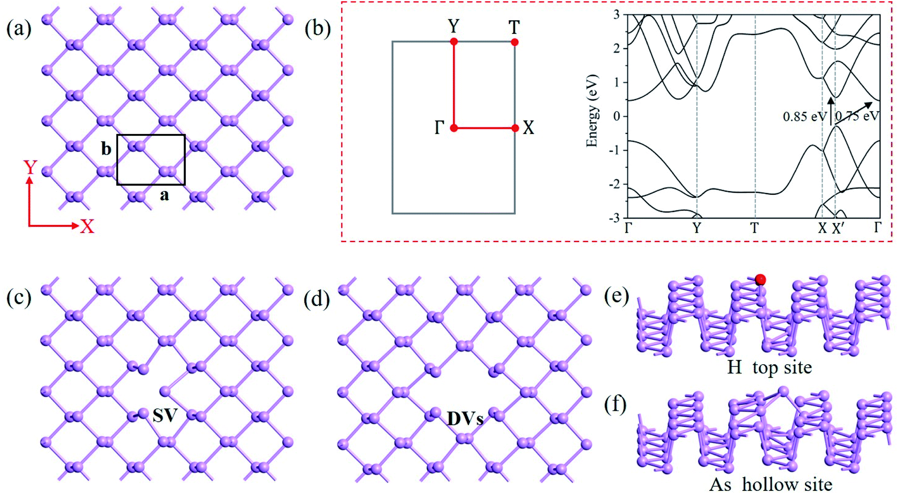 | ||
| Fig. 1 (a) The 4 × 4 orthorhombic supercell of arsenene monolayer. The black rectangle denotes the unit cell of arsenene. (b) High symmetry points in the first Brillouin zone and band structure of arsenene. (c) Single vacancy defect in arsenene. (d) Double vacancies in arsenene. (e) H adatom adsorbed on the top of the As atom (top site). (f) As adatom adsorbed above the hexagon of arsenene (hollow site). | ||
We use a 4 × 4 supercell to model the defects in arsenene monolayer. As shown in Fig. 1(c) and (d), we remove one and two As atoms from the center of the supercell to simulate the single vacancy (SV) and double vacancies (DVs), respectively. There is another type double vacancy defect formed by two adjacent vacancies in the top layer. This defect causes significant structure distortion around it, introduces no mid-gap state in the band gap region (see Fig. S1 in ESI†). We speculate that it has little contribution to improve the transport and will not be considered here. The optimized adsorption configurations of different adatoms are depicted in Fig. 1(e) and (f). H atom prefers to adsorb on top of an As atom of the arsenene (denoted as top site), while As and Li atoms prefer to adsorb above the hollow of the hexagon (denoted as hollow site). We determine the stability of the defect systems by calculating the formation energies ΔEform of vacancies or the adsorption energies ΔEads of adsorption atoms. The formation energy ΔEform is defined as ΔEform = Edefect − Earsenene + nEAs, where Edefect and Earsenene represent the total energies of monolayer arsenene with and without defects, respectively, EAs represents the average energy of each As atom in pristine arsenene, and n represents the number of missing As atoms for the vacancies. The adsorption energy is defined as ΔEads = Edefect − Earsenene − EX, where EX represents the energy of an isolated atom. As seen in Table 1, the formation energy of SV is 0.93 eV, smaller than that in phosphorene (1.63–1.64 eV) from previous calculation.38,39 This is consistent with that arsenene is more stable than phosphorene. The formation energy of DVs is almost twice of SV in both arsenene and phosphorene.38,39 This indicates that the relative stableness of vacancies is similar in both materials. The negative adsorption energies of H, As, and Li adatoms indicate stable adsorption of these atoms on arsenene monolayer. The H adatom adsorption energy in arsenene is similar to that in phosphorene of −1.37 eV.29
| Defect | SV | DVs | H | As | Li |
|---|---|---|---|---|---|
| ΔEform/ΔEads (eV) | 0.93 | 1.90 | −1.68 | −2.10 | −2.18 |
Fig. 2 shows the projected density of states (PDOSs) of arsenene with and without defects. The PDOS with SV defect in Fig. 2(a) is projected on the three As atoms around the vacancy. These As atoms move inward towards the center of the vacancy and induce defect states near CBM and VBM. The defect states near VBM are half occupied and the Fermi level shifts downwards near VBM. Thus SV can be regarded as a p-type defect. As shown in Fig. 2(b), the DVs defect introduces a high peak in the middle of the band gap. With one H adatom, one defect state is in the gap and near VBM as seen in Fig. 2(c). By introducing two H adatoms in the 4 × 4 supercell, we obtain four stable configurations (denoted as 2H_a, 2H_b, 2H_c, and 2H_d in Fig. S2 in ESI†). In 2H_a defect, two defect related peaks can be observed as shown in Fig. 2(d), one located within the valence band and the other in the band gap region. 2H_b and 2H_d defects also introduce mid-gap states in the band gap region, while 2H_c defect introduces a defect state just below the CBM (Fig. S3 in ESI†). The defect states introduced by one As adatom are near VBM, and the Fermi level is shifted downwards near VBM as shown in Fig. 2(e). In contrast, the Li adatom related defect states are near CBM and the Fermi level shifts upwards to CBM (Fig. 2(f)). Therefore, the As adatom can be considered as a p-type dopant, while the Li adatom is an n-type dopant. The type of the defects and the position of the related defect states may have different effects on the transport properties of n- and p-type devices, providing a possible way to tune the performance of the devices.30
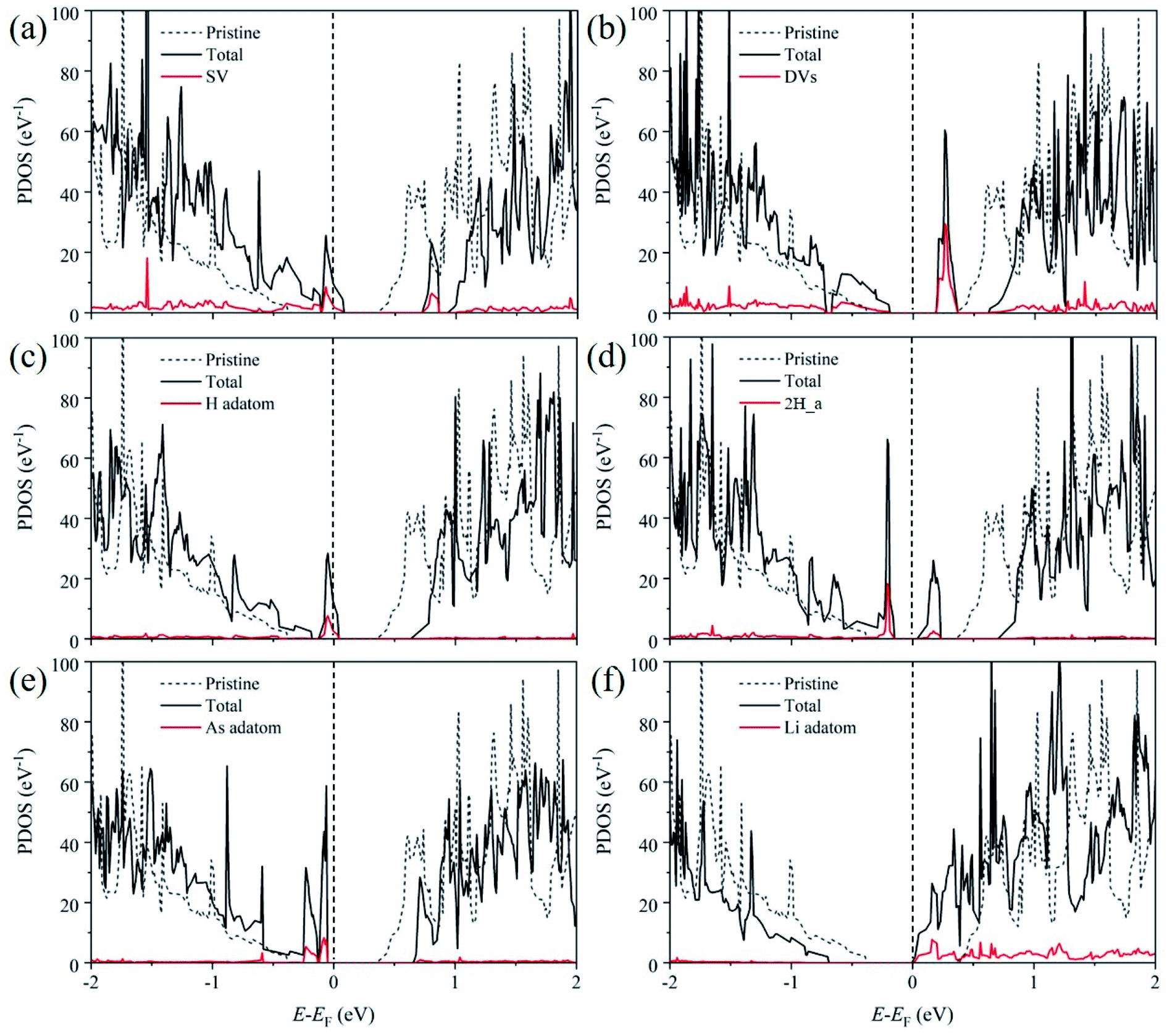 | ||
| Fig. 2 PDOSs of arsenene monolayer with different defects. (a) SV, (b) DVs, (c) H adatom, (d) 2H_a defect, (e) As adatom, and (f) Li adatom. The Fermi level EF is set as energy zero. The density of states of pristine arsenene are presented by dashed lines for comparison. | ||
We then construct arsenene TFETs to investigate the influences of different defects on the performance of the TFET devices. To build the arsenene TFET devices, we add the periodic arsenene on the left and right ends of the channel to simulate the semi-infinite electrodes. Considering the remarkable anisotropy in carrier mobilities and conductivities of arsenene,6 we simulate the double gate TFETs along two different transport directions, i.e., the armchair and zigzag directions. As shown in Fig. 3, the channel length along the transport direction is 8.8 nm in both cases. We introduce defects at the interface between the source and channel, as denoted by the red rectangles in Fig. 3. For the devices along the armchair transport direction, there are a total of 318 atoms for the pristine device. The defect concentrations with one and two adatoms adsorption are 0.31% and 0.63%, respectively. Along the zigzag transport direction, there are a total of 256 atoms for the pristine device, and the defect concentrations with one and two adatoms are 0.39% and 0.78%, respectively. Previous studies have demonstrated that the defects located at the source-channel interface can improve the performance of TFET devices based on 2D materials.29–32 The mid-gap states at the source-channel interface introduced by suitable defects can effectively shorten the tunneling path between the valence and conduction bands, facilitating the carrier tunneling from the source to the channel at the ON-state. The enhancement of the ON-state currents indicates a rapid transit from OFF-state to ON-state, resulting in a steeper SS. Here we aim to improve the performance of the arsenene TFET devices through defect modulation to meet the requirements of ITRS 2022 for HP or LP devices. For HP devices, VOFF is defined as the gate voltage with the OFF-state current IOFF at 0.1 μA μm−1. For LP devices, VOFF is the gate voltage with IOFF at 2 × 10⁻⁵ μA μm−1. The ON-state current ION is defined as the current at the gate voltage of VON = VOFF + Vds.
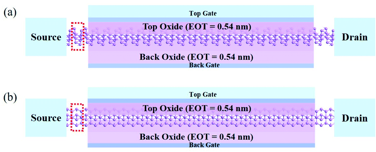 | ||
| Fig. 3 Schematics of the double gate arsenene TFET devices along the (a) armchair and (b) zigzag directions. Defects are introduced at the source-channel interface denoted by red rectangles. | ||
Fig. 4 shows current–voltage (I–Vg) characteristics of the arsenene TFET devices with and without defects along the armchair and zigzag directions. For the pristine devices, it can be seen that the currents along the armchair direction are always larger than those along the zigzag direction for both the n- and p-type TFETs (black curves in Fig. 4). This can be attributed to the anisotropy of the effective mass of the arsenene monolayer. In general, a smaller effective mass usually leads to a larger current for both bulk and 2D materials.5,22,40–44 As discussed earlier, the effective masses of electrons and holes along the armchair direction are overall smaller than those along the zigzag direction in arsenene. Therefore, the currents along the armchair direction are consistently larger than those along the zigzag direction for the pristine TFETs.
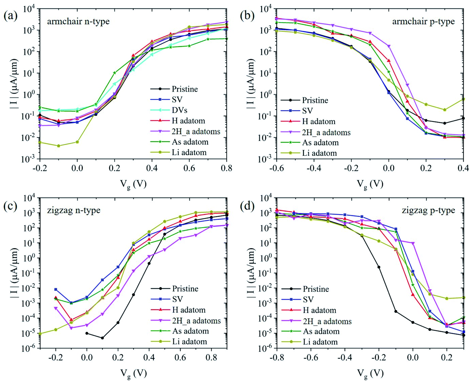 | ||
| Fig. 4 Current–voltage characteristics of the arsenene TFET devices with and without defects. (a) The n-type devices along armchair direction. (b) The p-type devices along armchair direction. (c) The n-type devices along zigzag direction. (d) The p-type devices along zigzag direction. | ||
Table 2 summarizes the performance of the arsenene TFET devices with and without defects along the armchair direction. For the pristine arsenene TFETs, the ON-state currents are still smaller than the ITRS 2022 requirement of 1330 μA μm−1 for HP devices. As seen in Table 2, the ON-state currents are 1132 and 1214 μA μm−1 for the n- and p-type TFETs, respectively. The corresponding ION/IOFF ratios are also slightly below the ITRS 2022 target of 1.33 × 10⁴. The SS values are 70 and 83 mV/decade for n- and p-type TFETs, respectively. Previous theoretical study reported a similar SS value of 75 mV decade−1 for arsenene MOSFET with a longer channel length of 10 nm along the same transport direction, and a larger SS over 100 mV decade−1 for shorter channel length.22 Although the arsenene TFETs have similar ON-state currents and better SS compared to the MOSFETs, their performance should be further improved for applications.
| Defects | Devices | SS (mV decade−1) | I OFF (μA μm−1) | I ON (μA μm−1) | I ON/IOFF |
|---|---|---|---|---|---|
| Pristine | n-type | 70 | 0.1 | 1132 | 1.13 × 10⁴ |
| SV | p-type | 83 | 0.1 | 1214 | 1.21 × 10⁴ |
| n-type | 77 | 0.1 | 1108 | 1.11 × 10⁴ | |
| p-type | 75 | 0.1 | 1084 | 1.08 × 10⁴ | |
| DVs | n-type | — | 0.18 | — | — |
| p-type | — | — | — | — | |
| H | n-type | 59 | 0.1 | 1412 | 1.41 × 10⁴ |
| p-type | 55 | 0.1 | 3564 | 3.56 × 10⁴ | |
| 2H_a | n-type | 89 | 0.1 | 2372 | 2.37 × 10⁴ |
| p-type | 50 | 0.1 | 3384 | 3.38 × 10⁴ | |
| As | n-type | 61 | 0.17 | — | — |
| p-type | 53 | 0.1 | 2286 | 2.29 × 10⁴ | |
| Li | n-type | 68 | 0.1 | 1837 | 1.84 × 10⁴ |
| p-type | 118 | 0.19 | — | — | |
| ITRS 2022 HP | 0.1 | 1330 | 1.33 × 10⁴ |
It can be seen from Table 2 that the defects could have a significant influence on the performance of the arsenene TFETs along the armchair transport direction. SV defect has no obvious effects on the performance for both n- and p-type devices. The mid-gap defect states introduced by DVs greatly reduce the bandgap and increase the OFF-state current to 0.18 μA μm−1, larger than the required 0.1 μA μm−1 for HP devices. Therefore, this defect will not be considered in the following calculations. On the other hand, the half-filled defect states introduced by one H adatom can significantly improve the overall performance for both n- and p-type devices. With one H atom adsorbed at the source-channel interface, ION of the n-type (p-type) arsenene TFET is increased to 1412 (3564) μA μm−1, ION/IOFF ratio increased to 1.41 × 10⁴ (3.56 × 10⁴), and the SS value reduced to 59 (55) mV decade−1. Clearly, both the n- and p-type devices with one H adatom meet the ITRS 2022 requirements for HP devices, and the SS value is reduced to below the 60 mV decade−1 limit. Increasing the H concentration might improve the performance. For example, 2H_a defect introduces two mid-gap states near the Fermi level as shown in Fig. 2(d). As a result, the ION and ION/IOFF values can be further increased for both n- and p-type TFETs. SS for p-type TFET can be reduced to 50 mV decade−1. However, SS for n-type TFET becomes larger than the pristine device.
The influence of defects highly depends on the types of the defects and the devices. We find that the p-type dopant As adatom can improve the performance of p-type TFET, but is unfavorable for n-type TFET. As seen in Table 2, p-type TFET with As defect exceeds the ITRS 2022 requirements for HP devices, whereas the n-type TFET has a large OFF-state current, failing to meet the ITRS 2022 requirements. Similarly, Li atom as an n-type dopant can improve the performance of the n-type TFET, but degrades the performance of the p-type TFET by increasing the OFF-state current.
Table 3 summarizes the performance of the arsenene TFET devices with and without defects along the zigzag direction. Due to the larger effective mass along the zigzag direction, the pristine arsenene TFETs have smaller ON-state currents and much smaller OFF-state currents, and meet the ITRS 2022 requirements for LP devices. The ON-state currents are 707 and 500 μA μm−1 for the n- and p-type TFETs, respectively, satisfying the ITRS 2022 requirement of 461 μA μm−1 for LP devices. The ION/IOFF ratios also exceed the required value of 2.31 × 10⁷. Besides, the small OFF-state currents lead to a rapid transit to the OFF-state. As a result, the pristine TFETs along the zigzag direction have very steep SSs. The SS values are 49 and 34 mV decade−1 for n- and p-type TFETs, respectively.
| Defects | Devices | SS (mV decade−1) | I OFF (μA μm−1) | I ON (μA μm−1) | I ON/IOFF |
|---|---|---|---|---|---|
| Pristine | n-type | 49 | 2 × 10⁻⁵ | 707 | 3.54 × 10⁷ |
| SV | p-type | 34 | 2 × 10⁻⁵ | 500 | 2.50 × 10⁷ |
| n-type | 65 | 0.1 | 412 | 4.12 × 10³ | |
| p-type | 36 | 2 × 10⁻⁵ | 851 | 4.26 × 10⁷ | |
| H | n-type | 56 | 0.1 | 1160 | 1.16 × 10⁴ |
| p-type | 34 | 0.1 | 1563 | 1.56 × 10⁴ | |
| 2H_a | n-type | 57 | 0.1 | 201 | 2.01 × 10³ |
| p-type | 31 | 0.1 | 942 | 9.42 × 10³ | |
| As | n-type | 70 | 0.1 | 188 | 1.88 × 10³ |
| p-type | 29 | 0.1 | 900 | 9.00 × 10³ | |
| Li | n-type | 33 | 2 × 10⁻⁵ | 500 | 2.50 × 10⁷ |
| p-type | 67 | 0.1 | 547 | 5.47 × 10³ | |
| ITRS 2022 HP | 0.1 | 1330 | 1.33 × 10⁴ | ||
| ITRS 2022 LP | 2 × 10⁻⁵ | 461 | 2.31 × 10⁷ |
Similar to the devices along the armchair direction, defects have a significant influence on the performance of the arsenene TFETs along the zigzag direction. SV introduces p-type defect states near VBM, and slightly increases the ON-state current of the p-type TFET to 851 μA μm−1, resulting in a larger ION/IOFF ratio of 4.26 × 10⁷. Meanwhile, the SS value is hardly influenced. For the n-type TFET, SV increases the OFF-state current to over 2 × 10⁻⁵ μA μm−1 due to the defect states near CBM (Fig. 2(a)), failing to meet the ITRS 2022 requirement for LP device. Yet its ON-state current is much less than the ITRS 2022 requirement for HP device. Therefore, SV as a p-type defect is only beneficial to the p-type arsenene TFETs along the zigzag direction.
The adsorption of one H adatom can increase both the ON-state and OFF-state currents of the arsenene TFETs along the zigzag direction, expanding their applications to HP devices. For n-type TFET, ION is increased to 1160 μA μm−1, still below the ITRS 2022 requirement. For p-type TFET, ION is increased to 1563 μA μm−1, with a small SS similar to the pristine p-type TFET. In other words, the p-type TFET with one H adatom can meet the ITRS 2022 requirements for HP devices. For all the adsorption of two H adatoms, our simulations show that 2H defects could partially improve the performance, depending on the defect configurations. The SS values of both n-type and p-type devices with 2H_a defect are better than 60 mV decade−1. The p-type devices with other 2H defects also have SS values below 60 mV decade−1 (see Fig. S5 and Table S1 in ESI†). However, all the devices have smaller ON-state currents than the devices with one H adatom, failing to meet the ITRS 2022 requirements. Therefore, increasing the defect concentration does not always lead to an improvement of the performance of the TFET devices.
As seen in Table 3, the p-type dopant As adatom is beneficial to the p-type TFET, decreasing the SS to 29 mV decade−1. However, the OFF-state current becomes larger than 2 × 10⁻⁵ μA μm−1, not suitable for LP device. The ION and ION/IOFF are not large enough to meet the requirements of ITRS 2022 for HP devices. Therefore, the As adatom is not a suitable defect to improve the performance of arsenene TFETs along the zigzag direction. The n-type dopant Li adatom is beneficial to the n-type TFET. With ION of 500 μA μm−1, ION/IOFF ratio of 2.50 × 10⁷, and a steep SS of 33 mV decade−1, the n-type TFET with Li defect can satisfy the requirements of ITRS 2022 for LP devices.
To analyze the defect assisted tunneling mechanism, we plot the projected local density of states (PLDOSs) of the pristine and defected arsenene TFET devices at OFF- and ON-states. Fig. 5 shows the PLDOSs for n-type TFETs along the armchair direction. The pristine arsenene TFET has a long tunneling path at OFF-state as shown in Fig. 5(a). At ON-state, the gate voltage shifts the channel conduction band downwards to overlap with the source valence band as shown in Fig. 5(b). The tunneling path becomes very short, allowing the band-to-band tunneling from the source to the channel. The considered defects at the source-channel interface could introduce defect states in the source-channel transition region. If the defect states happen to be in the overlapped window between the source and channel bands at ON-state, the effective tunneling length would be further decreased and the band-to-band tunneling currents could be remarkably enhanced.32 This is indeed the case for one H adatom defect (0.39% concentration). As shown in Fig. 5(d), the mid gap states introduced by the H adatom lie in the tunneling window at the ON-state, greatly enhancing the tunneling currents from the source to the channel. On the other hand, the defect states near the source VBM just slightly decrease the tunneling path at the OFF-state, as shown in Fig. 5(c). Therefore, the device can still maintain a small OFF-state current similar to the pristine TFET. The small OFF-state current and the enhanced ON-state current lead to a steeper SS below 60 mV decade−1. The H adatom defect shows a similar influence on the performance of the p-type TFET. The H defect state is close to the valence band and thus has a good overlap with the channel valence band at ON-state. Consequently, the ON-state current of the p-type TFET is enhanced to 3564 μA μm−1, even larger than that of the n-type device.
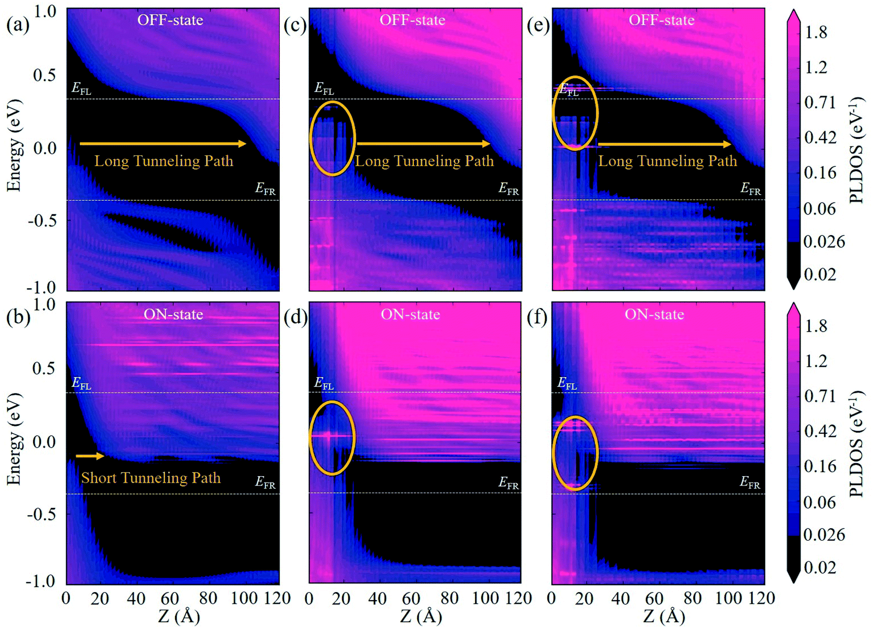 | ||
| Fig. 5 PLDOSs of the n-type arsenene TFETs along the armchair transport direction at OFF- and ON-states. (a) PLDOSs of pristine arsenene TFET at OFF-state. (b) PLDOSs of pristine arsenene TFET at ON-state. (c) PLDOSs of TFET with one H adatom at OFF-state. (d) PLDOSs of TFET with one H adatom at ON-state. (e) PLDOSs of TFET with 2H_a defect at OFF-state. (f) PLDOSs of TFET with 2H_a defect at ON-state. The orange ovals highlight the defect states at the source-channel interface. | ||
By introducing 2H_a defect at the source-channel interface (0.63% concentration), two defect states appear in the band gap region. For the n-type TFET at the ON-state, the two defect states enter the tunneling window as shown in Fig. 5(f). Therefore, the ON-state current is greatly enhanced to 2372 μA μm−1, larger than the device with one H adatom. At the OFF-state, the defect states just slightly decrease the tunneling path as shown in Fig. 5(e), similar to the one H adatom defect. And the device can still maintain a small OFF-state current below 0.1 μA μm−1. For the p-type TFET, only the upper defect state enters the tunneling window at the ON-state (not shown). And the ON-state current is 3384 μA μm−1, slightly smaller than the p-type device with one H adatom.
Next, we use As and Li defects to study the different influences on the device by n- and p-type dopants. The As adatom is a p-type dopant in arsenene. As shown in Fig. 6(a), the tunneling path of the n-type TFET at the OFF-state is obviously shortened due to the defect states near VBM induced by the As adatom, leading to a large leakage current above 0.1 μA μm−1. In other words, the p-type As dopant degrades the performance of the n-type TFET by increasing the OFF-state currents. For the p-type TFET at OFF-state, the As defect states near source VBM have very little influence on the tunneling path as shown in Fig. 6(b), maintaining a small OFF-state current. On the other hand, the As defect states at the ON-state lie in the tunneling window between the source and the channel as shown in Fig. 6(c), and thus can effectively enhance the ON-state currents. The rapid increase of the current also leads to a steeper SS of 53 mV decade−1. Therefore, the p-type As dopant is beneficial to the p-type TFETs by improving the ON-state currents as well as the SSs. On the contrary, the n-type Li adatom is beneficial to the n-type TFETs. As shown in Fig. 6(d), the defect states of the n-type Li adatom lie outside the tunneling window when the n-type device is at the OFF-state, maintaining a small OFF-state current below 0.1 μA μm−1. At the ON-state shown in Fig. 6(e), the Li defect states shift within the tunneling window resulting in a rapid increase of the ON-state currents. However, for the p-type device at the OFF-state shown in Fig. 6(f), the Li defect states lie within the tunneling window and shorten the tunneling path, and the OFF-state current exceeds 0.1 μA μm−1.
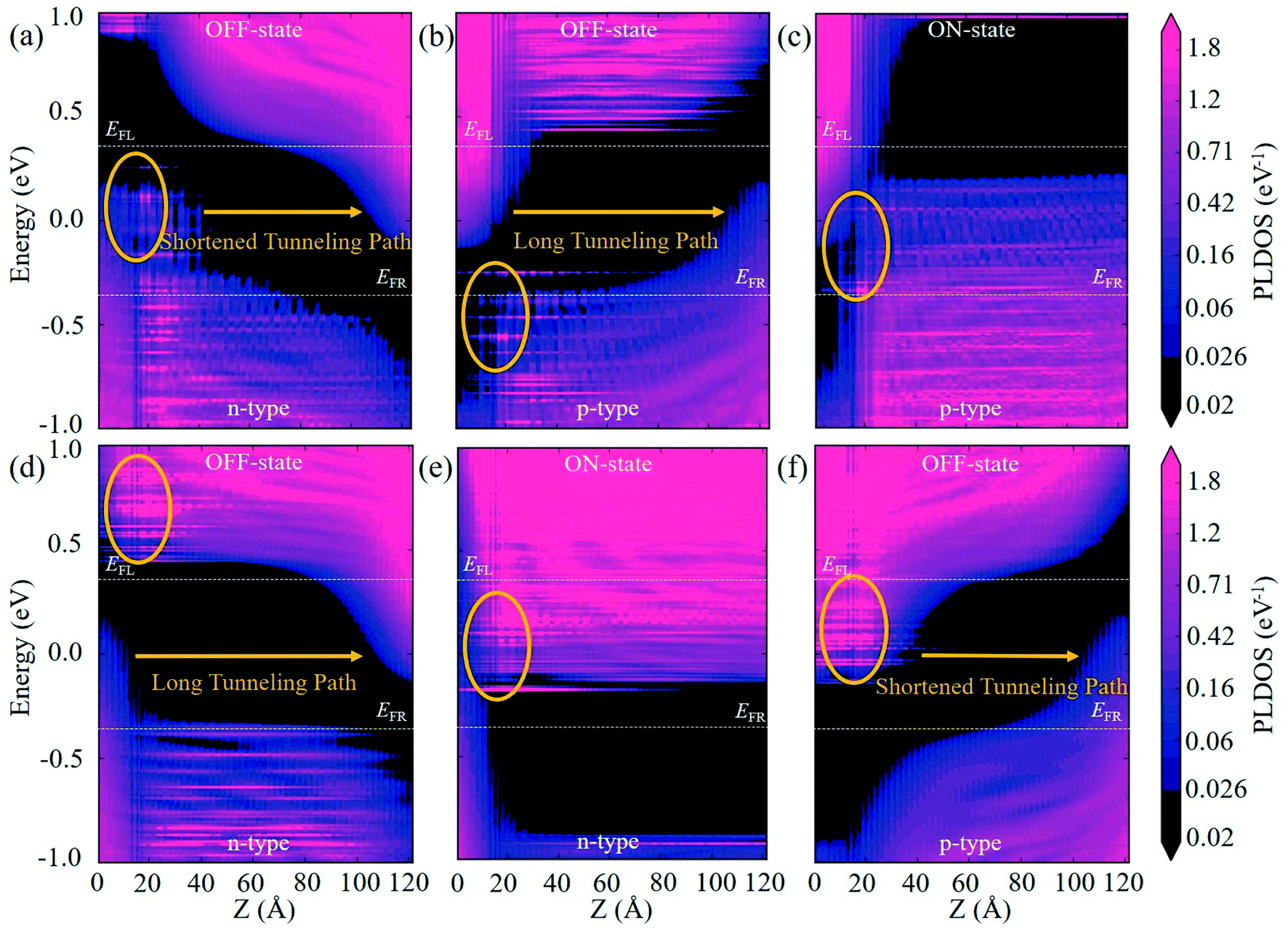 | ||
| Fig. 6 PLDOSs of the n- or p-types arsenene TFETs along the armchair transport direction at OFF- and ON-states. (a) PLDOS of n-type TFET with one As adatom at OFF-state. (b) PLDOSs of p-type TFET with one As adatom at OFF-state. (c) PLDOSs of p-type TFET with one As adatom at ON-state. (d) PLDOSs of n-type TFET with one Li adatom at OFF-state. (e) PLDOSs of n-type TFET with one Li adatom at ON-state. (f) PLDOS of p-type TFET with one Li adatom at OFF-state. | ||
Conclusion
In summary, we have systematically investigated the effects of different types of defects on the performance of arsenene TFETs through first-principles calculations and quantum transport simulations. We confirm the high anisotropy of the transport properties of arsenene TFETs along the armchair and zigzag directions. By introducing suitable defects at the source-channel interface, the performance of arsenene TFETs can be significantly improved to meet the ITRS 2022 requirements for HP or LP devices. For TFETs along the armchair directions, the adsorption of one and two H adatoms can significantly increase the ON-state currents and reduce SS to below 60 mV decade−1. The p-type dopant As and the n-type dopant Li can improve the performance of p-type and n-type devices, respectively, satisfying the ITRS 2022 requirements for HP devices. The arsenene TFETs along the zigzag direction already meet the ITRS 2022 requirements for LP devices. SV and As adatom as p-type defects can further increase the ON-state currents and/or reduce the SSs of the p-type LP TFETs. On the other hand, the adsorption of one H adatom can remarkably increase the ON-state current of the p-type TFET to 1563 μA μm−1 and reduce SS to 34 mV decade−1, allowing the device to work as an HP device. Our studies reveal the influence of different defects on the performance of arsenene TFETs and can be used as a theoretical guide to improve the performance of TFETs based on arsenene or other group VI monolayers by suitable defects.Conflicts of interest
There are no conflicts of interest to declare.Acknowledgements
This work was supported by the National Key R&D Program of China (Grant No. 2018YFB2202801) and the National Natural Science Foundation of China (Grants No. 11964022 and 12074369).References
- A. H. Castro Neto, F. Guinea, N. M. R. Peres, K. S. Novoselov and A. K. Geim, Rev. Mod. Phys., 2009, 81, 109–162 CrossRef CAS.
- H. O. Churchill and P. Jarillo-Herrero, Nat. Nanotechnol., 2014, 9, 330–331 CrossRef CAS PubMed.
- Q. H. Wang, K. Kalantar-Zadeh, A. Kis, J. N. Coleman and M. S. Strano, Nat. Nanotechnol., 2012, 7, 699–712 CrossRef CAS PubMed.
- A. J. Mannix, B. Kiraly, M. C. Hersam and N. P. Guisinger, Nat. Rev. Chem, 2017, 1, 0014 CrossRef CAS.
- Z. Zhang, J. Xie, D. Yang, Y. Wang, M. Si and D. Xue, Appl. Phys. Express, 2015, 8, 055201 CrossRef.
- Y. Chen, C. Chen, R. Kealhofer, H. Liu, Z. Yuan, L. Jiang, J. Suh, J. Park, C. Ko, H. S. Choe, J. Avila, M. Zhong, Z. Wei, J. Li, S. Li, H. Gao, Y. Liu, J. Analytis, Q. Xia, M. C. Asensio and J. Wu, Adv. Mater., 2018, 30, 1800754 CrossRef PubMed.
- L. Li, Y. Yu, G. J. Ye, Q. Ge, X. Ou, H. Wu, D. Feng, X. H. Chen and Y. Zhang, Nat. Nanotechnol., 2014, 9, 372–377 CrossRef CAS PubMed.
- M. H. Guimaraes, H. Gao, Y. Han, K. Kang, S. Xie, C. J. Kim, D. A. Muller, D. C. Ralph and J. Park, ACS Nano, 2016, 10, 6392 CrossRef CAS PubMed.
- H. L. Tang, M. H. Chiu, C. C. Tseng, S. H. Yang, K. J. Hou, S. Y. Wei, J. K. Huang, Y. F. Lin, C. H. Lien and L. J. Li, ACS Nano, 2017, 11, 12817–12823 CrossRef CAS PubMed.
- M. Zhong, Q. Xia, L. Pan, Y. Liu, Y. Chen, H.-X. Deng, J. Li and Z. Wei, Adv. Funct. Mater., 2018, 28, 1802581 CrossRef.
- W. Hong, G. W. Shim, S. Y. Yang, D. Y. Jung and S. Y. Choi, Adv. Funct. Mater., 2018, 29, 1807550 CrossRef.
- B. Wu, R. Quhe, J. Yang, S. Liu, J. Shi, J. Lu and H. Du, Adv. Theory Simul., 2020, 4, 2000238 CrossRef.
- S. Zhang, S. Guo, Z. Chen, Y. Wang, H. Gao, J. Gomez-Herrero, P. Ares, F. Zamora, Z. Zhu and H. Zeng, Chem. Soc. Rev., 2018, 47, 982–1021 RSC.
- J. Kang, W. Liu, D. Sarkar, D. Jena and K. Banerjee, Phys. Rev. X, 2014, 4, 031005 CAS.
- J. Qiao, X. Kong, Z. X. Hu, F. Yang and W. Ji, Nat. Commun., 2014, 5, 4475 CrossRef CAS PubMed.
- V. Tran, R. Soklaski, Y. Liang and L. Yang, Phys. Rev. B: Condens. Matter Mater. Phys., 2014, 89, 235319 CrossRef.
- J. O. Island, G. A. Steele, H. S. J. v. d. Zant and A. Castellanos-Gomez, 2D Mater., 2015, 2, 011002 CrossRef.
- C. Kamal and M. Ezawa, Phys. Rev. B: Condens. Matter Mater. Phys., 2015, 91, 085423 CrossRef.
- L. Kou, Y. Ma, X. Tan, T. Frauenheim, A. Du and S. Smith, J. Phys. Chem. C, 2015, 119, 6918–6922 CrossRef CAS.
- K. Luo, S. Chen and C. Duan, Sci. China: Phys., Mech. Astron., 2015, 58, 087301 Search PubMed.
- C. Wang, Q. Xia, Y. Nie, M. Rahman and G. Guo, AIP Adv., 2016, 6, 035204 CrossRef.
- H. Qu, Z. Lin, R. Guo, X. Ming, W. Zhou, S. Guo, X. Song, S. Zhang and H. Zeng, J. Semiconduct., 2020, 41, 082006 CrossRef CAS.
- K. P. Cheung, VLSI TSA, 2010, pp. 72–73 Search PubMed.
- R. Gandhi, Z. Chen, N. Singh, K. Banerjee and S. Lee, IEEE Electron Device Lett., 2011, 32, 437–439 CAS.
- R. Gandhi, Z. Chen, N. Singh, K. Banerjee and S. Lee, Sci. China Phys. Mech. Astron.Electron Device Lett., 2011, 32, 1504–1506 CAS.
- T. Nirschl, P.-F. Wang, C. Weber, J. Sedlmei, R. Heinrich, R. Kakoschke, K. Schriife, J. Holz, C. Pacha, T. Schulz, M. Ostermayr, A. Olbrich, G. Georgakos, E. Ruderer, W. Hansch and D. Schmitt-Landsiedel, IEDM Tech. Dig., 2004, 195–198 CAS.
- T. Krishnamohan, D. Kim, S. Raghunathan and K. Saraswat, IEDM Tech. Dig., 2008, 979–986 Search PubMed.
- C. Woo Young, P. Byung-Gook, L. Jong Duk and L. Tsu-Jae King, IEEE Electron Device Lett., 2007, 28, 743–745 Search PubMed.
- J. Lu, Z. Q. Fan, J. Gong, J. Z. Chen, H. ManduLa, Y. Y. Zhang, S. Y. Yang and X. W. Jiang, Phys. Chem. Chem. Phys., 2018, 20, 5699–5707 RSC.
- J. Wu, Z. Fan, J. Chen and X. Jiang, Appl. Phys. Express, 2018, 11, 054001 CrossRef.
- J. Wu, X. Ma, J. Chen and X. Jiang, Appl. Phys. Express, 2019, 12, 034001 CrossRef.
- X.-W. Jiang, J. Gong, N. Xu, S.-S. Li, J. Zhang, Y. Hao and L.-W. Wang, Appl. Phys. Lett., 2014, 104, 023512 CrossRef.
- Y. M. Takahiro Mori, N. Miyata, S. Migita, K. Fukuda, M. Masahara, T. Yasuda, and H. Ota, Symposium on VLSI Technology, IEEE, 2014, vol. 1 Search PubMed.
- M. Brandbyge, J.-L. Mozos, P. Ordejón, J. Taylor and K. Stokbro, Phys. Rev. B: Condens. Matter Mater. Phys., 2002, 65, 165401 CrossRef.
- J. P. Perdew, K. Burke and M. Ernzerhof, Phys. Rev. Lett., 1996, 77, 3865 CrossRef CAS PubMed.
- M. Buttiker, Y. Imry, R. Landauer and S. Pinhas, Phys. Rev. B: Condens. Matter Mater. Phys., 1985, 31, 6207–6215 CrossRef PubMed.
- P. M. Smith, A. J. Leadbetter and A. J. Apling, Philos. Mag., 1975, 31, 57–64 CrossRef CAS.
- W. Hu and J. Yang, J. Phys. Chem. C, 2015, 119, 20474–20480 CrossRef CAS.
- F. Zhan, W. Xu, R. Zou, J. Yang, J. Fan, X. Wu and R. Wang, J. Phys. Chem. C, 2019, 123, 27080–27087 CrossRef CAS.
- S. Liu, J. Yang, L. Xu, J. Li, C. Yang, Y. Li, B. Shi, Y. Pan, L. Xu, J. Ma, J. Yang and J. Lu, Nanoscale, 2021, 13, 5536–5544 RSC.
- Y. Guo, F. Pan, G. Zhao, Y. Ren, B. Yao, H. Li and J. Lu, Nanoscale, 2020, 12, 15443–15452 RSC.
- R. Quhe, Q. Li, Q. Zhang, Y. Wang, H. Zhang, J. Li, X. Zhang, D. Chen, K. Liu, Y. Ye, L. Dai, F. Pan, M. Lei and J. Lu, Phys. Rev. Appl., 2018, 10, 024022 CrossRef CAS.
- X. Sun, L. Xu, Y. Zhang, W. Wang, S. Liu, C. Yang, Z. Zhang and J. Lu, ACS Appl. Mater. Interfaces, 2020, 12, 20633–20644 CrossRef CAS PubMed.
- Y. Wang, R. Fei, R. Quhe, J. Li, H. Zhang, X. Zhang, B. Shi, L. Xiao, Z. Song, J. Yang, J. Shi, F. Pan and J. Lu, ACS Appl. Mater. Interfaces, 2018, 10, 23344–23352 CrossRef CAS PubMed.
Footnote |
| † Electronic supplementary information (ESI) available. See https://doi.org/10.1039/d2na00093h |
| This journal is © The Royal Society of Chemistry 2022 |