 Open Access Article
Graphene fibre film/polydimethylsiloxane nanocomposites for high-performance electromagnetic interference shielding†
Lu
Xu
,
Haohao
Lu
,
Yubing
Dong
,
Yaqin
Fu
and
Qingqing
Ni
 *
*
School of Materials Science and Engineering, Zhejiang Sci-Tech University, Hangzhou, Zhejiang 310018, China. E-mail: niqq@shinshu-u.ac.jp
First published on 29th June 2022
Abstract
Exploration of high-performance electromagnetic interference (EMI) shielding materials has become a trend to address the increasing electromagnetic (EM) wave pollution environment. In this paper, oriented graphene fibre film (GFF)/polydimethylsiloxane (PDMS) nanocomposites with one-ply unidirectional, two-ply cross-ply, and two-ply unidirectional configurations were prepared using wet-spinning and hot-pressing techniques in a two-step process. Due to the anisotropic electrical performance of GFF, the one-ply laminate exhibits EMI shielding anisotropy that is affected by fibre orientation relative to the electric field component in EM waves. The maximum shielding difference at 8.8 GHz is up to 32.0 dB between the fibre orientation parallel to and perpendicular to the electric field component. In addition, we found that adding a layer of GFF is an intuitive method to enhance the shielding efficiency (SE) of GFF/PDMS nanocomposites by providing more interfaces to enhance absorption losses. An optimal EMI shielding performance of a two-ply unidirectional laminate is observed with an SE value of 50.6 dB, which shields 99.999% of EM waves. The shielding mechanisms are also discussed and clarified from the results of both experimental and theoretical analyses by adjusting the GFF structural parameters, such as the fibre orientation, areal density, number of plies and stacking sequence.
1. Introduction
In recent years, with the rapid increase in data traffic and the popularity of portable electronic devices, the demand for electromagnetic interference (EMI) shielding of high-frequency systems has increased to address the increasingly complex electromagnetic (EM) wave pollution environment. EMI shielding materials, which attenuate EM waves to protect human health and the normal operation of precision devices, have attracted increasing attention.1–4 Traditionally, metal plates are commonly used as EMI shielding materials. However, the applications of metal-based EMI shielding materials in portable electronic devices and flexible electronic devices are limited due to their high weight density, low flexibility, and easy corrosion.5 In contrast, composite materials mixed with conductive fillers in resin materials have become a research hotspot in recent years due to their advantages of being lightweight and having good flexibility, corrosion resistance, and good mechanical properties.6–8 In particular, studies have reported various nanocarbon materials as functional fillers, such as carbon black (CB),9,10 carbon nanotubes (CNTs),11–13 graphene nanoplates (GNPs)14–17 and vapour-grown carbon fibres (VGCFs).18Due to their lamellar shape and high-aspect-ratio structure, GNPs are suitable for EMI shielding materials in applications requiring good conductivity.19 Therefore, many studies have reported composite materials with GNPs as conductive fillers.20–22 Although GNPs have a high conductivity due to the free movement of electrons over the π bond, commercial GNPs are synthesized as powder materials and therefore require a large fill concentration to breach the penetration threshold and form a conductive network.23 As a result, the conductivity of macroscopic composite materials is limited. In addition, as almost no active groups are present on the surface of GNPs, GNPs easily agglomerate in the materials, which not only decreases the conductivity but also forms defects in the composite materials.24 The electrical conductivity must be improved to enhance the interaction between electrons and electromagnetic fields and to obtain GNP/resin EMI shielding composites with excellent performance. From this perspective, achieving the orientation of GNPs in composites is a significant step towards preparing GNP-based EMI shielding composites. At present, many advanced processes have been developed for the preparation of oriented GNP structures. The graphene fibres (GFs) obtained using the wet-spinning process are a one-dimensional macroscopic assembly material composed of tightly arranged oriented GNPs, which inherits the excellent electrical conductivity of GNPs and has the potential to be an excellent candidate for conducting phases in composites.25,26
Extensive literature has shown that the orientation structure of carbon nanomaterials directly affects the direction dependence of EMI shielding performance. Lee et al. prepared an oriented CNT/PDMS nanocomposite for EM wave filtering using CNT films pulled from CNT forests.27 The difference in shielding effectiveness between the parallel alignments (2.0 dB) and the vertical alignments (10.0 dB) of CNTs reaches 8.0 dB. The highly oriented VGCFs/polyurethane (PU) nanocomposite fibrous membrane prepared by Yan et al. also has similar shielding properties.28 Variations in shielding effectiveness have been observed by changing the rotation angles of the VGCFs/PU fibrous membrane with the vibrational direction of EM waves, for which the shielding difference was greater than 10.0 dB (greater than 20.0 dB at 0°, less than 8.0 dB at 90°). Furthermore, Chikyu et al. prepared oriented CNT/polyethylene (PE) composite films and studied the effect of multilayer CNT structures on EMI shielding.29 The overall shielding performance and the corresponding reflection loss increase with an increasing number of CNT layers. Although some published reports have studied the unidirectional EMI shielding performance of carbon nanomaterials with different orientation structures and multilayer structures, the effects of the orientation structure, filler content, multilayer structure, and combination mode on the EMI shielding performance of composites have not been systematically summarized.
In the present study, GF films (GFFs) with different areal densities were prepared using the wet-spinning technique. GFF/polydimethylsiloxane (PDMS) nanocomposites were obtained by encapsulating oriented GFFs within PDMS. Then, the EMI shielding performance of GFF/PDMS nanocomposites with one-ply unidirectional, two-ply cross-ply, and two-ply unidirectional configurations was examined using a vector network analyser in wave-guide mode. The relationship between GFF structural parameters (such as the fibre orientation, areal density, number of plies, and stacking sequence) and the shielding performance of GFF/PDMS nanocomposites is established. The shielding mechanisms were also discussed and clarified from the results of both experimental and theoretical analyses, which provide a theoretical basis for designing high-performance EMI shielding materials.
2. Experimental section
2.1 Materials
The raw graphene oxide (GO) solution (solid concentration = 1%, sheet size = 5–40 μm) was supplied by Ang Xing Novel Carbon Material Changzhou Co. Ltd, China. Polydimethylsiloxane (PDMS) was supplied by Shenzhen Hongyejie Co. Ltd, China. Calcium chloride (CaCl2, purity > 95%) was purchased from Hangzhou Gaojing Fine Chemical Industry Co. Ltd, China. Absolute ethanol (C2H6O, liquid concentration ≥ 99.7%) and hydroiodic acid (HI, purity ≥ 47%) were purchased from Aladdin Reagent, China. Ultra-pure water was purified using a laboratory water purification system.2.2 Preparation of graphene fibre films
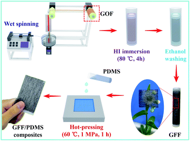
The graphene fibre film (GFF) was fabricated using wet spinning and chemical reduction techniques (see Fig. 1). First, a 3 wt% GO spinning solution was purified from a 1 wt% raw GO solution using a high-speed centrifuge at 18![[thin space (1/6-em)]](https://www.rsc.org/images/entities/char_2009.gif) 000 r per min for 2 h. Then, the resulting high-concentration spinning solution was packed into a glass injection tube with a needle diameter of 160 μm and an effective volume of 5 mL. Second, the GO fibres (GOFs) extruded from the needles were incubated in a rotating coagulation bath and collected on rollers. The coagulation bath solution was obtained by blending CaCl2 with ethanol and ultrapure water (5 wt% CaCl2, volume ratio of ethanol to water = 1
000 r per min for 2 h. Then, the resulting high-concentration spinning solution was packed into a glass injection tube with a needle diameter of 160 μm and an effective volume of 5 mL. Second, the GO fibres (GOFs) extruded from the needles were incubated in a rotating coagulation bath and collected on rollers. The coagulation bath solution was obtained by blending CaCl2 with ethanol and ultrapure water (5 wt% CaCl2, volume ratio of ethanol to water = 1![[thin space (1/6-em)]](https://www.rsc.org/images/entities/char_2009.gif) :
:![[thin space (1/6-em)]](https://www.rsc.org/images/entities/char_2009.gif) 3). Third, the GOFs were soaked in an HI solution at 60 °C for 4 h and reduced to graphene fibres (GFs). Then, GFs were repeatedly rinsed with anhydrous ethanol until I2 was completely removed from the fibres. Finally, the GFs were placed in a vacuum drying chamber at 60 °C and then cut to obtain complete GFFs. When the volume of the 3 wt% GO spinning solution was 5 mL, 10 mL, and 20 mL, the surface densities of the prepared GFFs were 5 gsm, 10 gsm, and 20 gsm, respectively.
3). Third, the GOFs were soaked in an HI solution at 60 °C for 4 h and reduced to graphene fibres (GFs). Then, GFs were repeatedly rinsed with anhydrous ethanol until I2 was completely removed from the fibres. Finally, the GFs were placed in a vacuum drying chamber at 60 °C and then cut to obtain complete GFFs. When the volume of the 3 wt% GO spinning solution was 5 mL, 10 mL, and 20 mL, the surface densities of the prepared GFFs were 5 gsm, 10 gsm, and 20 gsm, respectively.
2.3 Nanocomposite fabrication
The obtained one-ply GFFs were mixed with polydimethylsiloxane (PDMS) resin and placed into a 1 mm thick mould. Then, the whole mould was placed in a flat vulcanizing machine and cured for 1 h at 60 °C and 1 MPa to obtain one-ply unidirectional nanocomposites, as shown in Fig. 1. The two-ply cross-ply and two-ply unidirectional nanocomposites were prepared through the vertical and parallel lamination of two-ply GFFs using the same preparation process, respectively. The graphene contents of the nanocomposites with surface densities of 5 gsm, 10 gsm, and 20 gsm for monolayer GFF were 0.5 wt%, 1.0 wt%, and 2.0 wt%, respectively. The graphene content of the corresponding nanocomposites with double-layer GFF is 1.0 wt%, 2.0 wt%, and 4.0 wt%, respectively.2.4 Structural characterization
The cross-sectional morphology of the GFF/PDMS nanocomposites was studied using a scanning electron microscope (SEM, Ultra 55, Zeiss). The lay-up structure of graphene fibres in the PDMS matrix was observed using a polarizing microscope (PM, DM2007P, Leica Microsystems Co., Ltd, China) in transmission mode.2.5 Electrical performance test
The electrical conductivity (σ) of the GFFs with different areal densities was measured using a four-probe configuration (SZT-2B). The electrical conductivity of the GFFs in the 0°, 45°, and 90° directions was measured by rotating the GFFs to change the angle between the fibre orientation and the four probes (see Fig. S1†). The σ value was calculated using eqn (1): | (1) |
2.6 EMI shielding mechanisms
The electromagnetic wave is composed of in-phase oscillation and mutually perpendicular electric and magnetic fields moving in the form of waves in space, and its propagation direction is perpendicular to the plane composed of electric and magnetic fields. The EMI shielding mechanisms of shielding materials include reflection (SER), absorption (SEA), and multiple reflections (SEM) (see Fig. S2 in the ESI†). The shielding effectiveness was calculated using eqn (2).30–32 According to EMI shielding theory, the EMI shielding efficiency equation is derived as eqn (2):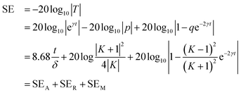 | (2) |
When the electromagnetic wave touches the shield layer, a portion of it is reflected because of the impedance mismatch between the free space and the shielding medium. The reflection formula is written as eqn (3):
 | (3) |
The SER values are calculated based on the assumption that ηs ≪ η0 using eqn (4):
 | (4) |
Eqn (4) shows that the greater the difference between η0 and ηs, the more electromagnetic waves are reflected at the interface.
The impedance is calculated using the following equation:
 | (5) |
The intrinsic impedance of free space (equivalent to materials with poor conductivity (σ = 0), such as air) and shielding medium (equivalent to materials with good conductivity) is calculated using eqn (6) and (7):
 | (6) |
 | (7) |
Some EM waves enter the interior of materials and interact with electrical or magnetic dipoles to convert them into other forms of energy (such as heat), which is called absorption. The distance at which the incident EM wave intensity is reduced to 1/e is defined as the skin depth and written as eqn (8):
 | (8) |
The absorption loss formula in shielding effectiveness is rewritten as eqn (9):
 | (9) |
Multiple reflection loss is attributed to the EM waves repeatedly hitting the wall in the shielding layer and is written as eqn (10). Multiple reflections are negligible when the SEA value reaches above 15 dB.
 | (10) |
2.7 EMI shielding measurement
The scattering parameters (S11, S12, S21, and S22) were measured by the coaxial transmission line method using a rectangular waveguide and a vector network analyser (see Fig. S3–S6 in the ESI†). The EMI SE is calculated using the following equation with four S parameters:| R = |S11|2 = |S22|211 |
| T = |S12|2 = |S21|212 |
| A = 1 − R − T13 |
| SE(%) = (1 − |S12|2) × 100%14 |
SER = −10![[thin space (1/6-em)]](https://www.rsc.org/images/entities/char_2009.gif) log10(1 − |S11|2) = −10 log10(1 − |S11|2) = −10![[thin space (1/6-em)]](https://www.rsc.org/images/entities/char_2009.gif) log10(1 − |S22|2)15 log10(1 − |S22|2)15 |
SET = −10![[thin space (1/6-em)]](https://www.rsc.org/images/entities/char_2009.gif) log10(|S12|2) = −10 log10(|S12|2) = −10![[thin space (1/6-em)]](https://www.rsc.org/images/entities/char_2009.gif) log10(|S21|2)16 log10(|S21|2)16 |
| SEA = SET − SER17 |
The electromagnetic field in the rectangular waveguide is a polarized electromagnetic field, wherein the direction of the short side of the rectangle is the electric field component, and the direction of the long side of the rectangle is the magnetic field component, as shown in Fig. S4–S6† in the ESI.†
3. Results and discussion
3.1 Electrical conductivity and composite structure
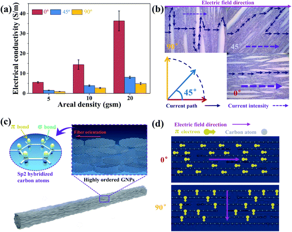
As conductive layers of nanocomposites, the electrical properties of GFFs are the decisive factor in the EMI shielding performance of GFF/PDMS nanocomposites. In our previous study, we showed that GFFs were completely reduced by recording XPS, Raman, and XRD spectra.33 The electrical conductivity of GFFs with different area densities in the directions of 0°, 45°, and 90° is shown in Fig. 2a. Corresponding specific data are shown in Table S1 of the ESI.† The experimental results show that GFFs have obvious anisotropic electrical conductivity. The electrical conductivity of the 20 gsm areal density GFF in the direction of 0° is 4.50 and 7.35 times that in the direction of 45° (8.08 S m−1) and 90° (4.94 S m−1), respectively. The electrical conductivities of the 5 and 10 gsm GFFs differ by 5.90 and 5.31 times between the 0° and 90° directions, respectively.The anisotropic electrical conductivity of GFFs is closely related to the atomic structure and fibre distribution (see Fig. 2b–d). On the one hand, the atomic structure consisting of a large number of highly ordered graphene nanoplates formed by sp2-hybridized carbon atoms containing strong σ bonds and delocalized π bonds within a hexagonal lattice supplies the graphene nanoplates with extensive free π electrons that are responsible for the high longitudinal conductivity of the graphene fibres.34 The carriers migrate at high speed without energy dissipation when the fibre orientation is parallel to the direction of the electric field (0°). As the fibre orientation deviates from the direction of the electric field, the conductive mechanism is transformed into the jumping of charge carriers between graphene nanosheets, and the resistivity increases considerably.35 On the other hand, the many larger elongated holes created by the fibre distribution arranged perpendicular to the axis substantially alter the electron propagation paths in all directions of the GFFs, as shown in Fig. 2b.33 As the fibre orientation gradually deviates from the direction of the electric field, the carrier transport path on the GFFs gradually increases due to the existence of these larger elongated holes, resulting in an increase in resistance.
In addition, the electrical conductivity of the GFFs increases as the areal density increases. In the 0° direction, the electrical conductivity of 20 gsm GFFs (36.33 S m−1) is 2.52 and 6.55 times that of 10 gsm GFFs (14.43 S m−1) and 5 gsm GFFs (5.55 S m−1), respectively. This phenomenon is due to the greater areal density of graphene fibres, a greater number of graphene fibres distributed per unit area, and a greater number of conductive channels.36
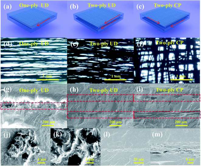
The GFFs in various lay-up configurations were encapsulated by PDMS to prepare one-ply unidirectional (UD), two-ply unidirectional, and two-ply cross-ply (CP) nanocomposites, as shown in Fig. 3a–c. The lay-up configurations of the GFF/PDMS nanocomposites were observed using PM and SEM, as shown in Fig. 3d–m. Compared with one-ply UD laminates, two-ply UD and two-ply CP laminates have double-layer GFFs with overlapping angles of 0° and 90°, respectively. In all samples, the diameter of all graphene fibres was uneven due to the irregular collapse of graphene nanoplates in graphene fibres and the fusion of two or more graphene fibres during the reduction process. The spacing between the radial distribution of graphene fibres is not uniform because of the elongated holes of different sizes. The high magnification image shows that the graphene nanoplates are completely infiltrated by the PDMS matrix and no cavities between the graphene nanoplates and the matrix could be observed in Fig. 4j and k. The individual graphene fibre without fusion has an effective diameter of 8 μm with a wrinkled surface and multilamellar structure. Furthermore, the graphene nanoplates protrude from the cross-section surface and are arranged in order along the fibre axis, as observed in the radial-section surface image (see Fig. 4m).
3.2 Electromagnetic interference shielding performance
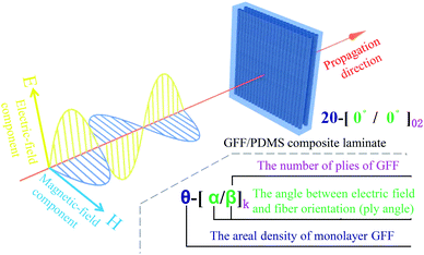
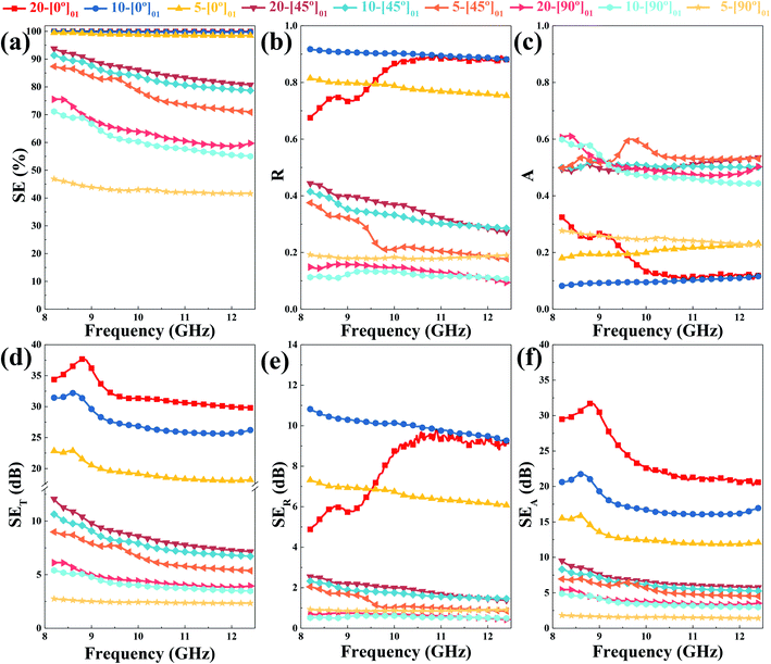
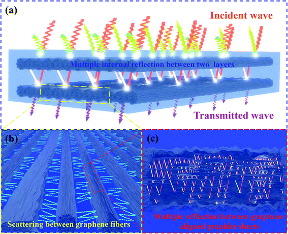
In this section, the EMI shielding characteristics of GFF/PDMS nanocomposites are investigated in relation to the lay-up configuration, and the interaction mechanism between the microwave and GFF/PDMS nanocomposites is analysed. For convenience, we defined the naming rules for the test samples to distinguish the nanocomposites with different ply angles, areal densities, and number of plies, as shown in Fig. 4. Moreover, the ply angle is defined as the angle between the electric field in EM waves and the fibre orientation of the GFFs.In addition to the conductivity of GFF and the distribution of ordered fibres, the shielding performance of composite films is also closely related to the internal structure of fibres. The tightly aligned graphite sheets in graphene fibres are completely infiltrated by the polymer matrix that induces large interfacial polarisations as a source of electron accumulation, thereby enhancing the scattering and multiple reflections of EM waves due to impedance mismatch.47 The collection of microscale-diameter graphene sheets in fibres provides a large surface area that is attractive for shielding because it increases the number of interactions with EM waves.48,49 In addition, the microstructure of the graphene fibre surface, such as wrinkles, grooves, and other heterogeneous interfaces, synergistically enhances the interaction with EM waves.50
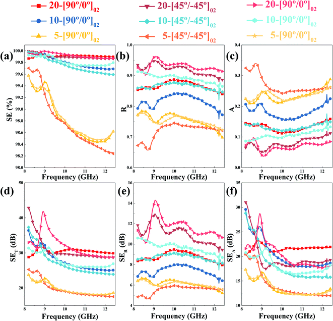
The interaction between EM waves and two-ply CP composite laminates is different in the three test directions, which is particularly evident in the differences in the contributions of reflection loss and absorption loss to radiation shielding, even if the baseline difference in the overall shielding performance is not large. For 20-[90°/0°]02 samples, the R and SER baselines are only 0.85 and 8.0 dB, respectively. In other words, this sample absorbed approximately 14.9% of the incident EM waves, a much higher proportion than the 20-[45°/−45°]02 and 20-[0°/90°]02 samples. This phenomenon is attributed to the perpendicular orientation of the first-layer GFFs in CP laminates to the electric field and the relatively high impedance matching degree, which ensures that the incident EM waves enter the material as much as possible and are absorbed by graphene fibres through scattering and multiple reflections.43 A sharp high resonance peak is formed on the SET curve of the 20-[90°/0°]02 sample, and the peak value is as high as 41.9 dB.
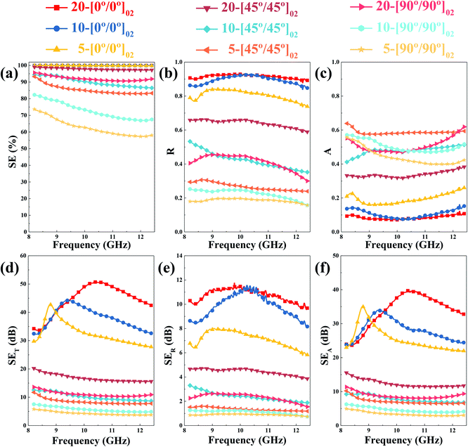
Double-layer GFFs with a low area density exert a better shielding effect when present in nanocomposites than single-layer GFFs with a high areal density. The SET curve of the 5-[0°/0°]02 samples in the x-band reaches more than 30.0 dB, and the maximum SET value is as high as 42.8 dB, which is much higher than that of the 10-[0°]01 sample. This significant increase is attributed to the provision of an extra interface at the same thickness of the shielding layer, which generates multiple reflections between the double layers and enhances the resonance effect.49 Furthermore, the A value of the 5-[0°/0°]02 samples (∼0.2) is higher than that of the 10-[0°]01 samples (∼0.1). This change in absorption loss is due to the poor electrical conductivity of low areal density GFFs, which improves the impedance mismatch (Fig. 8).46
Table 1 compares the EMI SE of GFF/PDMS composites with those of polymer-based composites that have been reported in the literature. In the literature, composite films with high EMI SE (exceeding 50 dB) were prepared by incorporating highly loaded conductive fillers into the resin.53,61,62 Additionally, we define the specific SE, given by EMI SE/thickness, to compare the shielding performance of composite films with various thicknesses. We emphasize that the GFF/PDMS composite films presented in this paper have higher specific SE at lower conductive filler loadings than those reported in the previous literature. The 20-[0°/0°]02 sample film has an EMI SE of 50.6 dB with a thickness of 1 mm, which corresponds to the specific SE of 50.6 dB mm−1, even a smaller graphene loading of 4 wt%.
| Sample | Filler fraction | Film thickness (mm) | EMI SE (dB) | SE/thickness (dB mm−1) | Year/reference |
|---|---|---|---|---|---|
| CF/EP | — | 1.1 | 36 | 32.7 | 2021/41 |
| CF/EP | — | 1.3 | 46.8 | 36 | 2015/51 |
| CNT/GO/EP | 15 wt% | 1 | 32 | 32 | 2018/52 |
| MWCNT/ABS | 15 wt% | 1.1 | 50 | 45.5 | 2013/53 |
| CNT/UHMWPE | 4 wt% | 1.6 | 32.6 | 20.4 | 2018/54 |
| CNT/UHMWPE | 2 wt% | 1 | 33.5 | 33.5 | 2019/55 |
| CNF/CPE | 10 wt% | 1 | 24 | 24 | 2017/56 |
| Graphene/PVA | 20 wt% | 2 | 39 | 19.5 | 2020/57 |
| CB/IR | 30 wt% | 1 | 26 | 26 | 2020/58 |
| MWCNT/PES/EP | 2.9 wt% | 2.2 | 23 | 10.5 | 2020/59 |
| CB/FCNF/CPE | 15 wt% | 1 | 33 | 33 | 2020/60 |
| CB/Fe3O4/PVDF | 40 wt% | 2 | 55.3 | 27.7 | 2020/61 |
| Ag/PLA | 5.89 vol% | 1.5 | 50 | 33.3 | 2018/62 |
| MXene/PS | 1.9 volt% | 2 | 62 | 31 | 2017/63 |
| Ag/EP | 20 wt% | 2 | 42 | 21 | 2019/64 |
| This work | 4 wt% | 1 | 50.6 | 50.6 | — |
Different from other homogeneous conductive fillers/polymer nanocomposites, the graphene nanocomposites proposed in this paper adopt GFF prepared by wet-spinning as conductive fillers, achieving a low permeability threshold and high electromagnetic shielding performance due to the tight orientation of 2D graphene sheets in the fibres. By controlling the surface density and configuration structure of GFF, the electrical and EMI shielding properties of graphene nanocomposites can be easily adjusted to suit the practical application environment. More importantly, due to its excellent spinnability and good binding force between graphene sheets, GFF can greatly improve the mechanical properties of graphene nanocomposites while providing shielding properties (GFF's mechanical properties are superior to those of other 2D nanosheet fibres, such as MXene fibres).65,66 This provides a new idea for designing lightweight and high mechanical strength EMI shielding composites.
4. Conclusions
In this study, we prepared oriented GFF/PDMS nanocomposites in which the shielding performance was optimized by changing the lay-up configuration and areal density of the GFFs using wet-spinning and hot-pressing techniques. The tight orientation of 2D graphene sheets in GFF/PDMS nanocomposites forms a stable conductive network layer, achieving a low permeability threshold and high electromagnetic shielding performance. The one-ply unidirectional GFF/PDMS nanocomposites exhibit EMI shielding anisotropy due to the existence of the anisotropic conductive network, and the maximum shielding difference at 8.8 GHz is as high as 32.0 dB between 0° and 90° ply angles. The functional transformation from unidirectional shielding to multidirectional shielding is achieved by adding an extra layer of orthogonal GFFs to the GFF monolayer. We also observed that the two-ply unidirectional configuration of GFF in the polymer matrix substantially improves the shielding performance in an absorption mode-enhanced manner through internal multiple reflections and resonance phenomena. The maximum SET value of two-ply unidirectional composites with 20 gsm GFFs is as high as 50.6 dB (the shielding efficiency is 99.999%) at 10.4 GHz and a 0° ply angle. Furthermore, the multilayer structure of GFFs with a low areal density substantially improves the shielding efficiency while improving impedance mismatch. The shielding mechanisms of GFF/PDMS nanocomposites were also discussed and clarified from the results of both experimental and theoretical analyses by adjusting the GFF structural parameters, which provided a scientific basis for the design of high-performance and functional electromagnetic interference shielding composites.Conflicts of interest
The authors declare no competing financial interest.Acknowledgements
This work was supported by the National Natural Science Foundation of China (Grant No. 52073259).References
- T. Yun, H. Kim, A. Iqbal, Y. S. Cho, G. S. Lee, M. K. Kim, S. J. Kim, D. Kim, Y. Gogotsi, S. O. Kim and C. M. Koo, Adv. Mater., 2020, 32, 1906769 CrossRef CAS PubMed.
- B. Yao, W. Hong, T. W. Chen, Z. B. Han, X. W. Xu, R. C. Hu, J. Y. Hao, C. H. Li, H. Li, S. E. Perini, M. T. Lanagan, S. L. Zhang, Q. Wang and H. Wang, Adv. Mater., 2020, 32, 1907499 CrossRef CAS PubMed.
- X. X. Wang, J. C. Shu, W. Q. Cao, M. Zhang, J. Yuan and M. S. Cao, Chem. Eng. J., 2019, 369, 1068–1077 CrossRef CAS.
- A. Iqbal, P. Sambyal and C. M. Koo, Adv. Funct. Mater., 2020, 30, 2000883 CrossRef CAS.
- M. K. Zhang, P. J. Zhang, Q. Wang, L. Li, S. J. Dong, J. Liu and W. Rao, J. Mater. Chem. C, 2019, 7, 10331–10337 RSC.
- D. W. Jiang, V. Murugadoss, Y. Wang, J. Lin, T. Ding, Z. C. Wang, Q. Shao, C. Wang, H. Liu, N. Lu, R. B. Wei, A. Subramania and Z. H. Guo, Polym. Rev., 2019, 59, 280–337 CrossRef CAS.
- C. Wang, V. Murugadoss, J. Kong, Z. F. He, X. M. Mai, Q. Shao, Y. J. Chen, L. Guo, C. T. Liu, S. Angaiah and Z. H. Guo, Carbon, 2018, 140, 696–733 CrossRef CAS.
- H. G. Liu, S. Q. Wu, C. Y. You, N. Tian, Y. Li and N. Chopra, Carbon, 2021, 172, 569–596 CrossRef CAS.
- J. Kruzelak, A. Kvasnicakova, K. Hlozekova, R. Dosoudil, M. Goralik and I. Hudec, Polymers, 2021, 13, 616 CrossRef CAS PubMed.
- R. Ravindren, S. Mondal, P. Bhawal, S. M. N. Ali and N. C. Das, Polym. Compos., 2019, 40, 1404–1418 CrossRef CAS.
- Z. H. Zeng, H. Jin, M. J. Chen, W. W. Li, L. C. Zhou and Z. Zhang, Adv. Funct. Mater., 2016, 26, 303–310 CrossRef CAS.
- Y. M. Huangfu, K. P. Ruan, H. Qiu, Y. J. Lu, C. B. Liang, J. Kong and J. W. Gu, Composites, Part A, 2019, 121, 265–272 CrossRef CAS.
- O. Pitkänen, J. Tolvanen, I. Szenti, A. Kukovecz, J. Hannu, H. Jantunen and K. Kordas, ACS Appl. Mater. Interfaces, 2019, 11, 19331–19338 CrossRef PubMed.
- Z. M. Fan, D. L. Wang, Y. Yuan, Y. S. Wang, Z. J. Cheng, Y. Y. Liu and Z. M. Xie, Chem. Eng. J., 2020, 381, 122696 CrossRef CAS.
- H. Jia, Q. Q. Kong, Z. Liu, X. X. Wei, X. M. Li, J. P. Chen, F. Li, X. Yang, G. H. Sun and C. M. Chen, Composites, Part A, 2020, 129, 105712 CrossRef CAS.
- Z. Yu, T. W. Dai, S. W. Yuan, H. W. Zou and P. B. Liu, ACS Appl. Mater. Interfaces, 2020, 12, 30990–31001 CrossRef CAS PubMed.
- V. T. Nguyen, B. K. Min, Y. Yi, S. J. Kim and C. G. Choi, Chem. Eng. J., 2020, 393, 124608 CrossRef CAS.
- M. Yuksek, J. Eng. Fibers Fabr., 2020, 15, 1558925020985959 CAS.
- M. S. Cao, X. X. Wang, W. Q. Cao and J. Yuan, J. Mater. Chem. C, 2015, 3, 6589–6599 RSC.
- H. Deng, L. Lin, M. Z. Ji, S. M. Zhang, M. B. Yang and Q. Fu, Prog. Polym. Sci., 2014, 39, 627–655 CrossRef CAS.
- H. M. Zhang, G. C. Zhang, Q. Gao, M. Zong, M. Y. Wang and J. B. Qin, Composites, Part A, 2020, 130, 105773 CrossRef CAS.
- G. L. Sang, J. W. Dong, X. T. He, J. C. Jiang, J. B. Li, P. Xu and Y. S. Ding, Composites, Part B, 2019, 164, 467–475 CrossRef CAS.
- H. M. Zhang, G. C. Zhang, M. Tang, L. S. Zhou, J. T. Li, X. Fan, X. T. Shi and J. B. Qin, Chem. Eng. J., 2018, 353, 381–393 CrossRef CAS.
- S. G. Prolongo, R. Moriche, A. Jiménez-Suárez, M. Sanchez and A. Urena, Eur. Polym. J., 2014, 61, 206–214 CrossRef CAS.
- Y. J. Liu, Z. Xu, W. W. Gao, Z. D. Cheng and C. Gao, Adv. Mater., 2017, 29, 1606794 CrossRef PubMed.
- Z. Xu, H. Y. Sun, X. L. Zhao and C. Gao, Adv. Mater., 2013, 25, 188–193 CrossRef CAS PubMed.
- D. W. Lee, J. Park, B. J. Kim, H. Kim, C. Choi, R. H. Baughman, S. J. Kim and Y. T. Kim, Carbon, 2019, 142, 528–534 CrossRef CAS.
- Y. J. Yan, H. Xia, Y. P. Qiu, Z. Z. Xu and Q. Q. Ni, Mater. Lett., 2019, 245, 98–102 CrossRef CAS.
- N. Chikyu, T. Nakano, G. Kletetschka and Y. Inoue, Mater. Des., 2020, 195, 108918 CrossRef CAS.
- W. L. Song, M. S. Cao, M. M. Lu, S. Bi, C. Y. Wang, J. Liu, J. Yuan and L. Z. Fan, Carbon, 2014, 66, 67–76 CrossRef CAS.
- R. Schulz, V. Plantz and D. Brush, IEEE Trans. Electromagn. Compat., 1988, 30, 187–201 Search PubMed.
- H. Bizhani, V. Nayyeri, A. Katbab, A. Jalali-Arani and H. Nazockdast, Eur. Polym. J., 2018, 100, 209–218 CrossRef CAS.
- L. Xu, H. H. Lu, Y. Zhou, Z. Y. Chi, Z. Li, Z. I. Md, Y. B. Dong, Y. Q. Fu, Y. F. Zhu and Q. Q. Ni, Adv. Mater. Technol., 2021, 6, 2100531 CrossRef CAS.
- Z. Xu and C. Gao, Mater. Today, 2015, 18, 480–492 CrossRef CAS.
- J. Hicks, A. Tejeda, A. Taleb-Ibrahimi, M. S. Nevius, F. Wang, K. Shepperd, J. Palmer, F. Bertran, P. Le Fevre, J. Kunc, W. A. de Heer, C. Berger and E. H. Conrad, Nat. Phys., 2013, 9, 49–54 Search PubMed.
- M. Rahaman, T. K. Chaki and D. Khastgir, Polym. Compos., 2011, 32, 1790–1805 Search PubMed.
- J. Song and P. Xu, Materials, 2021, 14, 1907 Search PubMed.
- C. L. Holloway, M. S. Sarto and M. Johansson, IEEE Trans. Electromagn. Compat., 2005, 47, 833–844 CrossRef.
- N. C. Das, D. Khastgir, T. K. Chaki and A. Chakraborty, Composites, Part A, 2000, 31, 1069–1081 CrossRef.
- J. M. Keith, N. B. Janda, J. A. King, W. F. Perger and T. J. Oxby, Polym. Compos., 2005, 26, 671–678 CrossRef CAS.
- J. Hong, P. Xu, H. Xia, Z. Z. Xu and Q. Q. Ni, Compos. Sci. Technol., 2021, 203, 108616 CrossRef CAS.
- A. Ameli, P. U. Jung and C. B. Park, Carbon, 2013, 60, 379–391 CrossRef CAS.
- H. G. Kim, H. J. Shin, G. C. Kim, H. J. Park, H. J. Moon and L. K. Kwac, Carbon Lett., 2014, 15, 268–276 CrossRef.
- D. Munalli, D. Chronopoulos and S. Greedy, In 9th European Workshop on Structural Health Monitoring 2018 Search PubMed.
- D. Munalli, G. Dimitrakis, D. Chronopoulos, S. Greedy and A. Long, Composites, Part B, 2019, 173, 106906 CrossRef.
- K. H. Wong, S. J. Pickering and C. D. Rudd, Composites, Part A, 2010, 41, 693–702 CrossRef.
- N. Yousefi, X. Y. Sun, X. Y. Lin, X. Shen, J. J. Jia, B. Zhang, B. Z. Tang, M. S. Chan and J. K. Kim, Adv. Mater., 2014, 26, 5480–5487 CrossRef CAS PubMed.
- D. G. Lai, X. X. Chen and Y. Wang, Carbon, 2020, 158, 728–737 CrossRef CAS.
- J. Li, D. Zhou, P. J. Wang, C. Du, W. F. Liu, J. Z. Su, L. X. Pang, M. S. Cao and L. B. Kong, Chem. Eng. J., 2021, 425, 131558 CrossRef CAS.
- D. X. Yan, H. Pang, B. Li, R. Vajtai, L. Xu, P. G. Ren, J. H. Wang and Z. M. Li, Adv. Funct. Mater., 2015, 25, 559–566 CrossRef CAS.
- X. M. Zhao, J. J. Fu and H. B. Wang, J. Ind. Text., 2016, 46, 45–58 CrossRef CAS.
- N. Ucar, B. K. Kayaoğlu, A. Bilge, G. Gurel, P. Sencandan and S. Paker, J. Compos. Mater., 2018, 52, 3341–3350 CrossRef CAS.
- M. H. Al-Saleh, W. H. Saadeh and U. Sundararaj, Carbon, 2013, 60, 146–156 CrossRef CAS.
- W. C. Yu, J. Z. Xu, Z. G. Wang, Y. F. Huang, H. M. Yin, L. Xu, Y. W. Chen, D. X. Yan and Z. M. Li, Composites, Part A, 2018, 110, 237–245 CrossRef CAS.
- W. C. Yua, G. Q. Zhang, Y. H. Liu, L. Xu, D. X. Yan, H. D. Huang, J. H. Tang, J. Z. Xua and Z. M. Li, Chem. Eng. J., 2019, 373, 556–564 CrossRef.
- S. Mondal, L. Nayak, M. Rahaman, A. Aldalbahi, T. K. Chaki, D. Khastgir and N. C. Das, Composites, Part B, 2017, 109, 155–169 CrossRef CAS.
- J. Joseph, A. Sharma, B. Sahoo, J. Paul and A. M. Sidpara, Mater. Today Commun., 2020, 23, 100941 CrossRef CAS.
- G. Wang, Q. Yu, Y. Hu, G. Zhao, J. Chen, H. Li, N. Jiang, D. Hu, Y. Xu, Y. Zhu and A. G. Nasibulin, Compos. Commun., 2020, 21, 100417 CrossRef.
- H. Zhang, Z. Heng, J. Zhou, Y. Shi, Y. Chen, H. Zou and M. Lian, Chem. Eng. J., 2020, 398, 125559 CrossRef CAS.
- S. Mondal, R. Ravindren, P. Bhawal, B. Shin, S. Ganguly, C. Nah and N. C. Das, Composites, Part B, 2020, 197, 108071 CrossRef CAS.
- L. Vidhya and G. Subodh, J. Electron. Mater., 2020, 49, 1666–1676 CrossRef.
- K. Zhang, H. O. Yu, K. X. Yu, Y. Gao, M. Wang, J. Li and S. Guo, Compos. Sci. Technol., 2018, 156, 136–143 CrossRef CAS.
- R. Sun, H. B. Zhang, J. Liu, X. Xie, R. Yang, Y. Li, S. Hong and Z. Z. Yu, Adv. Funct. Mater., 2017, 27, 1702807 CrossRef.
- X. Fan, G. Zhang, Q. Gao, J. Li, Z. Shang, H. Zhang, Y. Zhang, X. Shi and J. Qin, Chem. Eng. J., 2019, 372, 191–202 CrossRef CAS.
- Z. Xu, H. Sun, X. Zhao and C. Gao, Adv. Mater., 2013, 25, 188–193 CrossRef CAS PubMed.
- W. Eom, H. Shin, R. B. Ambade, S. H. Lee, K. H. Lee, D. J. Kang and T. H. Han, Nat. Commun., 2020, 11, 1–7 CrossRef PubMed.
Footnote |
| † Electronic supplementary information (ESI) available. See https://doi.org/10.1039/d2na00243d |
| This journal is © The Royal Society of Chemistry 2022 |

