
 Open Access Article
 This Open Access Article is licensed under a Creative Commons Attribution-Non Commercial 3.0 Unported Licence
Deformation twinning via the motion of adjacent dislocations in a nanostructured CoCrFeNi high-entropy alloy
Jinpo
Zhai
a,
Zhigang
Yan
 *b and
Hao
Yu
*a
*b and
Hao
Yu
*a
aSchool of Materials Science and Engineering, University of Science and Technology Beijing, Beijing, 100083, China. E-mail: yuhao@ustb.edu.cn
bAnalysis and Testing Center, Shenzhen Technology University, Shenzhen, Guangdong 518118, China. E-mail: yanzhigang@sztu.edu.cn
First published on 9th August 2022
Abstract
Deformation twinning was observed in a nanostructured CoCrFeNi high-entropy alloy processed by cold rolling. A three-layer twin with two incoherent twin boundaries was identified using high-resolution transmission electron microscopy, and its twinning mechanism was analyzed. Twinning is formed by dissociated dislocations meeting on the adjacent slip plane. This twinning mechanism possibly works for low-SF materials with high dislocation density.
Introduction
High-entropy alloys (HEAs) are a new class of alloys consisting of multiple (five and more) components in equimolar or near-equimolar ratios.1,2 In recent years, HEAs have attracted great attention due to their attractive properties such as high strength,3,4 high ductility,3,4 high hardness,5,6 high fracture toughness7 and ability to form nanoparticles for excellent durability electrocatalysts.8Twinning is a significant crystalline defect due to its potential to simultaneously improve the strength and ductility of nanostructured (NS) materials.9–14 High-strength nanotwinned Cu13 and gradient nanotwinned Cu14 with favorable ductility have been manufactured. In face-centered cubic (FCC) materials, twinning is generated by Shockley partial dislocations gliding on successive slip planes,9–11 and this deformation process is determined by the intrinsic material properties and deformation conditions. In general, a low stacking fault energy (SFE), nano-sized grain, high strain rate10,11 and cryogenic deformation10,11 promote the tendency of deformation twinning.
The twinning mechanisms have also been widely investigated. In coarse-grained materials, their dislocation sources locate at grain interiors, and twinning is generated by pole mechanisms,15 faulted dipoles16 and prismatic glide.17 When the grain size decreases to the nanoscale, grain boundaries (GBs) become the main dislocation sources, and twinning is generated differently. Zhu et al.18 proposed a dislocation reaction and cross-slip mechanism on the grain boundary. Narayan et al.19 proposed a cross-slip deformation twinning model. These mechanisms produce a macroscopic strain, which is not energetically favorable; therefore, they generally operate at high-stress conditions. Wu et al.20 proposed an energy-favorable twinning mechanism: the random activation of partials (RAP), wherein the Burgers vectors sum of twinning dislocations is zero and the twinning is of zero macroscopic strain. Wang et al.21 observed a new detwinning mechanism by the gliding of incoherent twin boundaries (ITBs). Liu et al.22 proposed that both twinning and detwinning mechanisms could be accomplished via the nucleation and migration of ITBs in low stacking fault energy metals. An et al.23 suggested that ITBs may be nucleated via the synchronized emission of three partials (b1:b2:b3) from a GB. This process is similar to the twinning mechanism via cooperatively activated partials (CAP),24 wherein three Shockley partial dislocations with a zero sum Burgers vector are activated synchronously. In addition, Shockley partial dislocations could be nucleated from two GBs in NS materials. In a related experimental study, Zheng et al.25 observed alternating emission mechanisms in nano-sized Cu/Nb multilayers; the formation of twinning was observed via the alternating emission mechanism over sequential emission of the same twinning dislocation on adjacent twinning planes. In another related study, Hunter et al.26 predicted that this alternating emission mechanism is energetically favorable because it accommodates strain yet removes debilitating backstresses. Zhang et al.27 investigated the twinning behavior in the CrCoNi medium-entropy alloy, where three-layer twinning can be formed by a three-layer stacking fault. Wang et al.28 observed deformation twinning initiated through the formation of two stacking faults separated by a single atomic layer, and proceeded with the emission of a partial dislocation in between these two stacking faults. Ding et al.29 observed that a nanotwin with three atomic layers is formed by three partial dislocations slip, and the Burgers vector of the three partial dislocations is zero.
Inspection of the published scientific literature indicates that GBs play an important role in the twinning of NS materials; deformation twinning is usually generated from the GBs. Interestingly, in the present cold rolled NS CoCrFeNi high-entropy alloy (HEA), nano-sized twinning was observed at the grain interiors. Its features were characterized by high-resolution TEM (HRTEM), and the twinning mechanism was analyzed and discussed.
Experimental
The CoCrFeNi HEA were prepared by arc-melting a mixture of pure metals under a high-purity argon atmosphere, and the HEA was re-melted 5 times to improve its chemical homogeneity. The ingot was homogenized at 1473 K for 12 h, followed by hot forging at 1273 K; the HEA was then cold rolled at room temperature with 82.5% reduction (to ∼1.67 mm). Tensile specimens with a gauge length of 9 mm and a width of 2 mm were cut from the cold rolled and annealed sheets, and the specimens were polished before the tensile tests. Tensile tests were conducted at a strain rate of 5 × 10⁻⁴ s−1 at room temperature using an Instron 5960 testing machine. The microstructures were characterized and HRTEM was performed on a Titan ETEM G2 apparatus. The TEM samples were prepared on a twin-jet electropolishing apparatus (Tenupol-5) using a solution of 5 vol% perchloric acid and 95 vol% ethanol at room temperature. Phase characterization was carried out by X-ray diffraction (XRD) using a Rigaku D/MAX-2500 diffractometer equipped with Cu radiation in a 2θ range from 20° to 120°.Results and discussion
Fig. 1a shows a typical planar-view scanning transmission electron microscopy (STEM) bright-field (BF) micrograph of the cold rolled HEA. The typical microstructures of cold rolled HEAs are very tiny and consist of nanograins (N), elongated nanograins (E) and nanotwins (NT). The chemical composition distribution of the HNS HEAs was measured by STEM EDS mapping as shown in Fig. 1b, showing the uniform distribution of all the principal elements. Fig. 1c shows the XRD pattern of the cold rolled HEAs. All the diffraction peaks can be indexed assuming a single face-centered cubic (FCC) phase. Representative tensile true stress vs. strain curves of the cold rolled (NS) HEAs at room temperature are shown in Fig. 1d. The NS HEAs exhibit high yield strength (∼1070 MPa) and high ultimate tensile strength (∼1250 MPa), but their ductility is very limited, and the uniform elongation and failure elongation are ∼1.8% and ∼11.5%, respectively.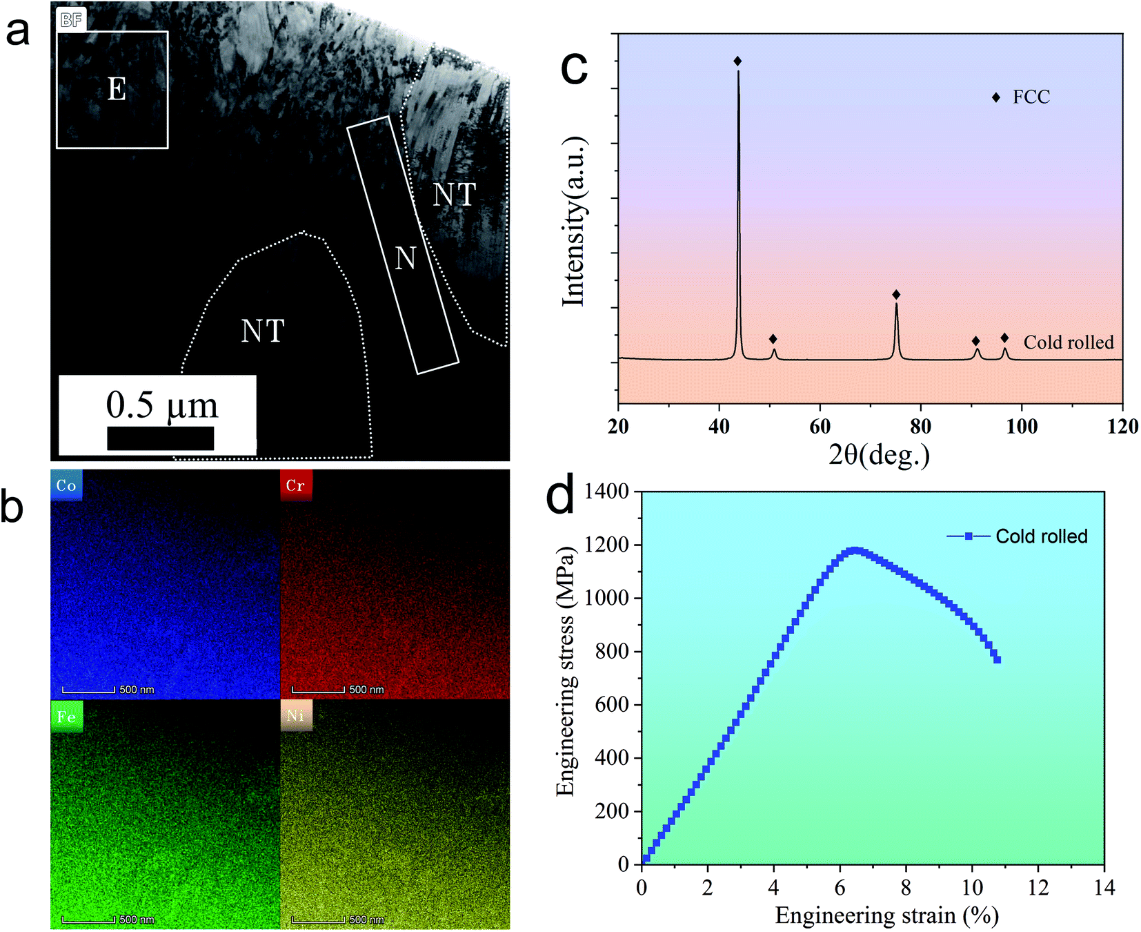 | ||
| Fig. 1 Microstructures of the cold rolled NS HEA: (a) STEM BF image of the cold rolled NS HEA, showing several micrometer-size grains with high dislocation density. (b) EDS maps of the cold rolled NS HEA, showing no deviation from the chemical composition. (c) XRD patterns of the cold rolled NS HEA, showing a single FCC structure. (d) Tensile engineering stress–strain curves of the cold rolled NS HEA. | ||
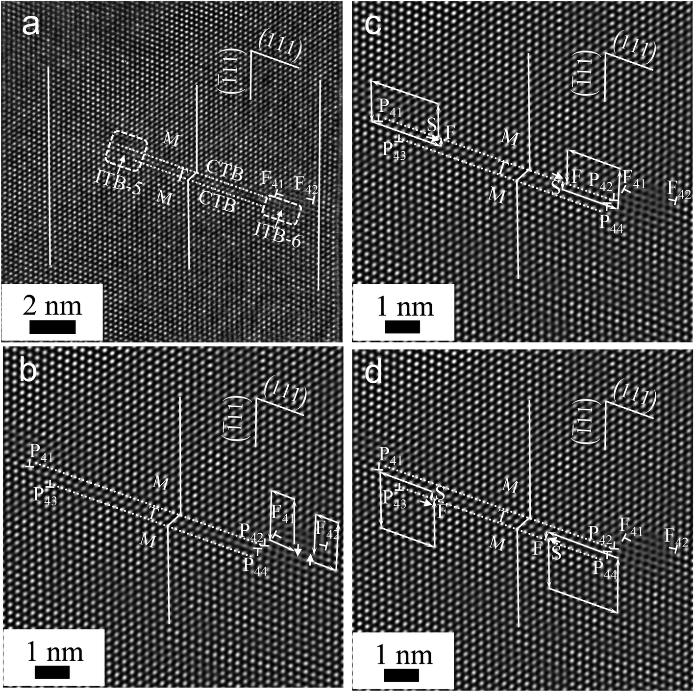
Fig. 2a shows a typical bright-field (BF) micrograph of the nanotwin lamellae in the cold rolled HEA as well as the selected area electron diffraction (SAED) pattern verifying the twinning relationship between the matrix and twin lamellae. The twin thicknesses fall in the range of ∼4 nm to ∼117 nm with the average grain size being ∼27 ± 5 nm, as shown in Fig. 2b. In addition, Fig. 2a presents the high density of dislocations at the lamellae interiors.
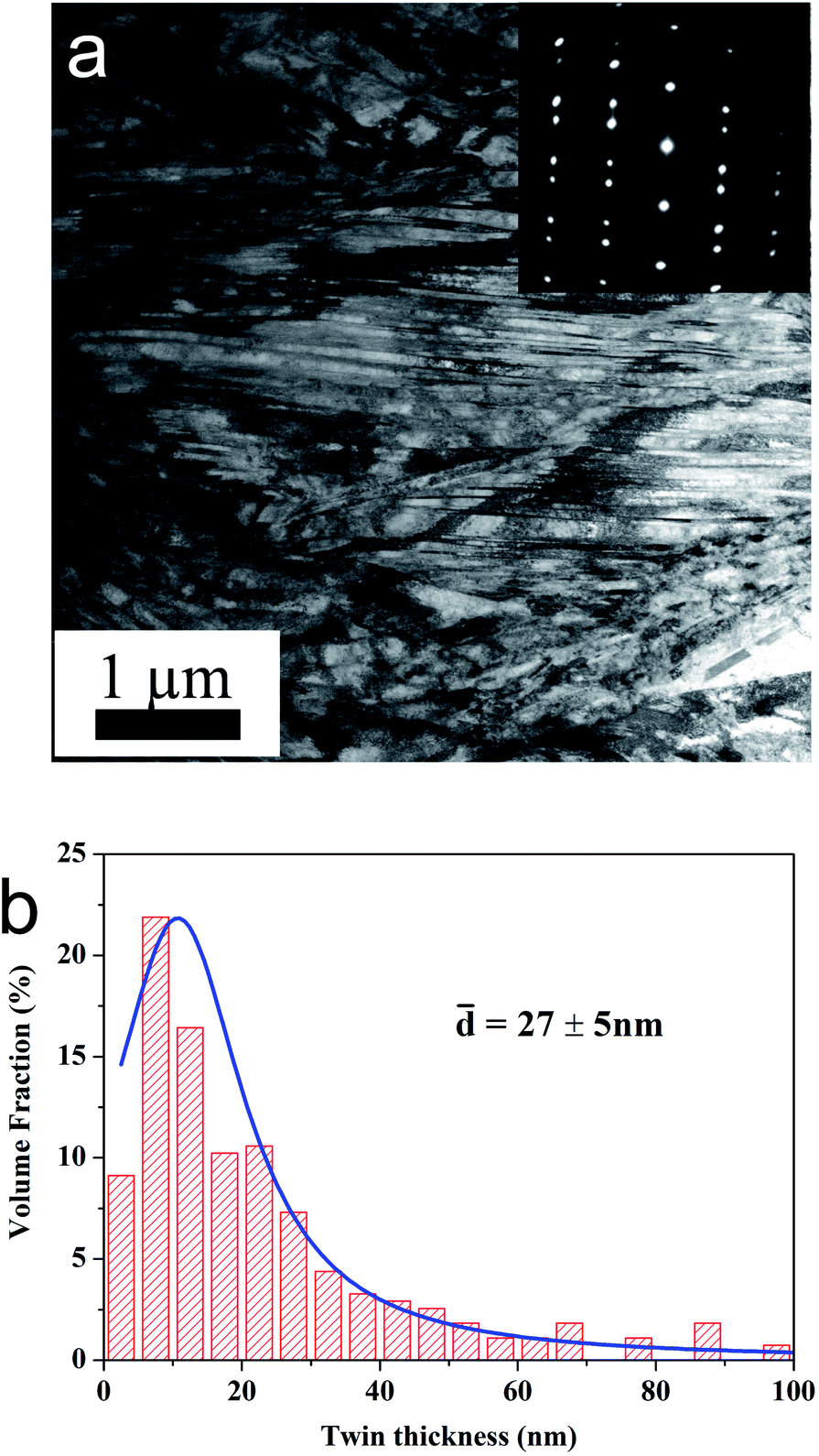 | ||
| Fig. 2 Microstructure of twinning in the cold rolled NS HEA: (a) typical TEM BF micrograph of twinning, showing a high density of dislocations at the twin interiors. (b) The twin thickness distribution. | ||
In order to observe the twin lamellae more clearly, HRTEM micrographs were obtained on the [01![[1 with combining macron]](https://www.rsc.org/images/entities/char_0031_0304.gif) ] axis. As shown in Fig. 3a, three coherent twin boundaries (CTBs) indicate that there are two nanotwins 6.2 nm and 18.3 nm in thickness, labeling with “T”. A plane defect with a width of 7.2 nm on the (111) plane is marked with a quadrilateral. Fig. 3b presents an enlarged image of the quadrilateral zone of Fig. 3a, which clearly shows that the plane defect is a three-layer twin enclosed with two incoherent twin boundaries (ITBs). The configurations of the two ITBs are different; the width of ITB-1 is shorter than that of ITB-2. Careful analysis indicates that the ITBs were composed of four partial dislocations: P21, P22, P23 and P24. To determine the types of the partial dislocations, the Burgers circuits of those dislocations were drawn (P21 and P23 in Fig. 3c; P22 and P24 in Fig. 3d). Then, the projection vectors of the Burgers vectors of the four dislocations on the (01) plane can be measured as
] axis. As shown in Fig. 3a, three coherent twin boundaries (CTBs) indicate that there are two nanotwins 6.2 nm and 18.3 nm in thickness, labeling with “T”. A plane defect with a width of 7.2 nm on the (111) plane is marked with a quadrilateral. Fig. 3b presents an enlarged image of the quadrilateral zone of Fig. 3a, which clearly shows that the plane defect is a three-layer twin enclosed with two incoherent twin boundaries (ITBs). The configurations of the two ITBs are different; the width of ITB-1 is shorter than that of ITB-2. Careful analysis indicates that the ITBs were composed of four partial dislocations: P21, P22, P23 and P24. To determine the types of the partial dislocations, the Burgers circuits of those dislocations were drawn (P21 and P23 in Fig. 3c; P22 and P24 in Fig. 3d). Then, the projection vectors of the Burgers vectors of the four dislocations on the (01) plane can be measured as 
 and
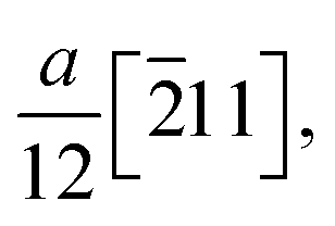
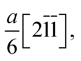
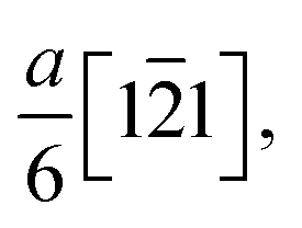
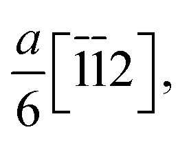
and  where a = 0.3559 nm30,31 is the lattice constant of the CoCrFeNi HEA, which corresponded to dislocations P21, P22, P23 and P24, as shown in Table 1. By matching the measured projection vectors with the calculated Burgers vectors of all of the possible partial dislocations present in FCC materials (ref. 32), the Burgers vectors of the four dislocations are determined to be
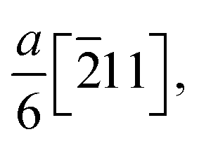
 and
and  corresponding to dislocations P21, P22, P23 and P24, as shown in Table 1.
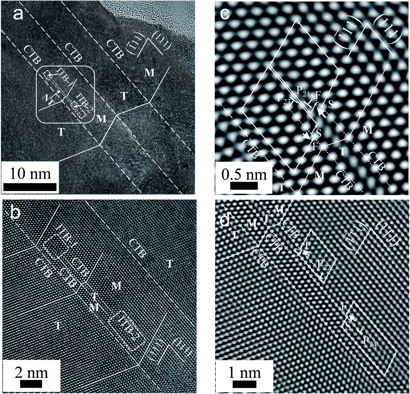 | ||
| Fig. 3 HRTEM of twinning in the cold rolled NS HEA: (a) low-magnification HRETM micrograph of the twins, showing the presence of plane defects marked using white squares. (b) High-magnification HRTEM micrograph of the square zone of (a), showing a 7.3 nm wide twin with two incoherent twin boundaries (ITBs). (c) Enlarged IFFT micrographs of ITB-1 containing the two partial dislocations with the surrounding Burgers circuits. (d) Enlarged IFFT micrographs of ITB-2 containing the two partial dislocations with the surrounding Burgers circuits. | ||
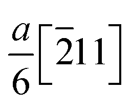


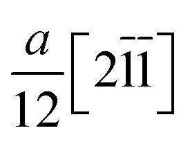
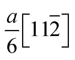

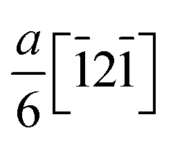

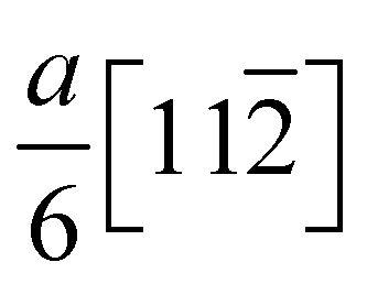


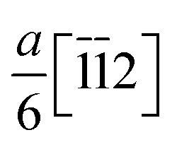


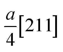
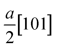
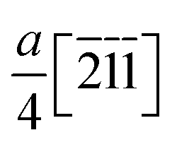
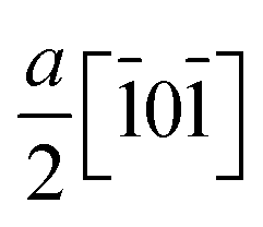

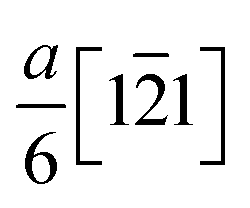

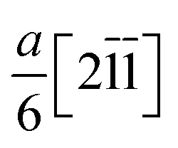
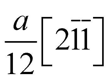

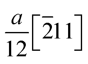
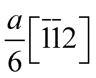
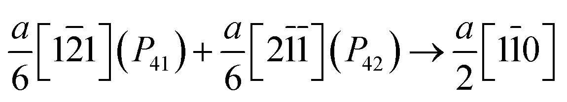
Fig. 4 presents a similar nanotwin with a width of 3.4 nm in the middle of a matrix lamella. The configuration of ITBs here is different from the ITBs in Fig. 3, although they have the same width. Further analysis of the structure of the two ITBs shows that they are composed of four partial dislocations: P31, P32, P33 and P34. The Burgers vectors were also determined by drawing Burgers circuits surrounding the partial dislocations, as shown in Fig. 4c and d. The Burgers vectors of the four dislocations are determined to be 

 and
and  corresponding to dislocations P31, P32, P33 and P34, as shown in Table 1.
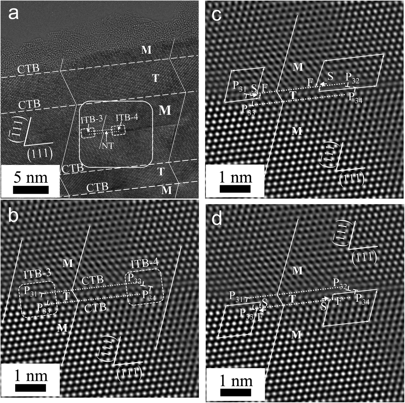 | ||
| Fig. 4 HRTEM of twinning in the cold rolled NS HEA: (a) low-magnification HRETM micrograph of the twins, showing the presence of plane defects marked using white squares. (b) High-magnification HRTEM micrograph of the square zone of (a), showing a 3.4 nm wide twin with two incoherent twin boundaries (ITBs). (c) IFFT micrographs of the nanotwin with the two Burgers circuits surrounding the two partial dislocations P31 and P32. (d) IFFT micrographs of the nanotwin with the two Burgers circuits surrounding the two partial dislocations P33 and P34. | ||
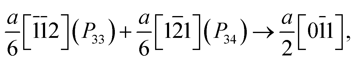
Fig. 5 presents another nanotwin configuration that consists of a 6.2 nm wide nanotwin and two full dislocations. The Burgers vectors of four partial dislocations in the ITBs and two full dislocations were identified. Their Burgers vectors are determined to be 
 and
and 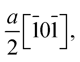 corresponding to dislocations P41, P42, P43, P44, F41 and F42, as shown in Table 1. Obviously, F41 and F42 have the same Burgers vector with opposite signs, and they locate at the adjacent slip plane ({111} plane) with ∼1.0 nm. Therefore, it can be determined that F41 and F42 constitute a dislocation dipole.
 | ||
| Fig. 5 (a) HRTEM micrograph of a 6.2 nm wide twin connected with two dislocations F41 and F42. (b) The Burgers circuits surrounding F41 and F42 and the enlarged IFFT micrographs of the nanotwin enclosed by four partial dislocations P41, P42, P43 and P44. (c) and (d) The Burgers circuits surrounding the dislocations. | ||
Discussion
In NS materials, twinning can be formed through a series of Shockley partials emitted from GBs. For the GBs to be partial dislocation sources, one of the twin boundaries must be on the GBs. This configuration has been verified by experiments and molecular dynamics (MD) simulations.18–26 In the present study, a three-layer twin was observed at the matrix interior with two ITBs. Therefore, it may be formed by other mechanisms. As Fig. 2 shows, a large number of dislocations are stored at the lamellae interiors. In low-SFE FCC materials, a full dislocation usually dissociates into two Shockley partials and an SF to a lower dislocation energy;17 when two dissociated dislocations meet on the adjacent slip plane, the parallel partial dislocations attract each other to reduce the lattice distortion and form a three-layer twin.Suppose the three-layer twin was formed by two full dislocations on the adjacent slip plane. The whole dislocation Burgers vector of the atomic (111) plane shown in Fig. 3 was calculated by the sum of partial dislocations: 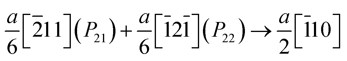 and
and 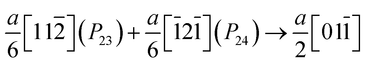 . Considering that the dislocation line aligns very closely to the direction of the electron beam33–36 [01],
 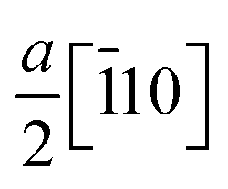 and
and  are a 60° full dislocation and a screw full dislocation, respectively.
The dislocation Burgers vectors of the atomic planes in Fig. 4 and 5 were also calculated: 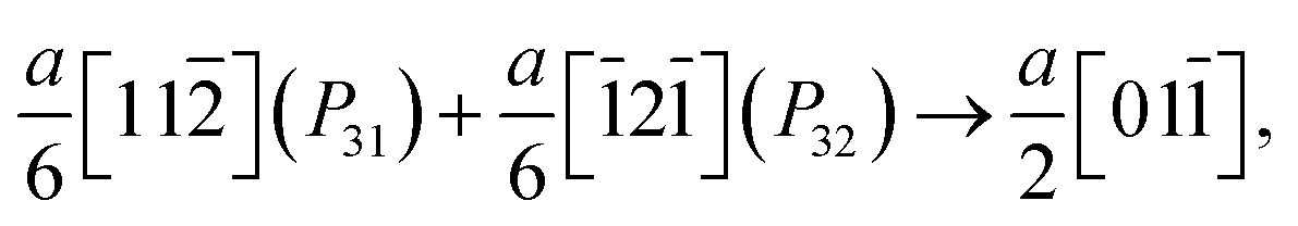
 and
and 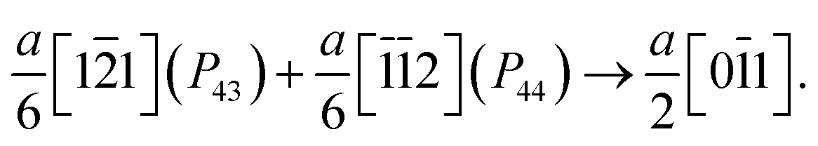 Clearly,
 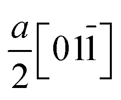 and
and 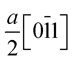 are two screw full dislocations, and
  is a 60° full dislocation. It can be concluded that the three-layer twin in Fig. 4 was formed by two screw dislocations, and the twin in Fig. 5 was formed by a 60° full dislocation and a screw dislocation.
The SF of the CoCrFeNi HEA has been calculated by density functional theory (DFT) simulations;37,38 its SF is only ∼34 mJ m−2. In such low SF metals, full dislocation dissociation is energetically favorable, and the equilibrium width of the dissociation SF can be calculated as follows:9
 | (1) |
In addition, partial dislocation pinned by faulted dipoles was observed in Fig. 5, indicating that gliding partial dislocations can be pinned on the slip plane by other defects, which increases the probability of interaction of the partial dislocations on the adjacent plane to generate a three-layer twin.
In summary, a three-layer twin has been observed in a cold rolled CoCrFeNi HEA, which may be formed by two dissociated full dislocations meeting on the adjacent slip plane. This twinning mechanism possibly works for low-SF materials with high dislocation density.
Conflicts of interest
There are no conflicts to declare.References
- J. W. Yeh, S. K. Chen, S. J. Lin, J. Y. Gan, T. S. Chin and T. T. Shun, et al. , Adv. Eng. Mater., 2004, 6, 299–303 CrossRef CAS.
- B. Cantor, I. T. Chang, P. Knight and A. J. Vincent, Mater. Sci. Eng., A, 2004, 375, 213–218 CrossRef.
- F. Otto, A. Dlouhý, C. Somsen, H. Bei, G. Eggeler and E. P. George, Acta Mater., 2013, 61, 5743–5755 CrossRef CAS.
- S. J. Sun, Y. Z. Tian, H. R. Lin, X. G. Dong, Y. H. Wang, Z. J. Zhang and Z. F. Zhang, Mater. Des., 2017, 133, 122–127 CrossRef CAS.
- O. N. Senkov, S. V. Senkova and C. Woodward, Acta Mater., 2014, 68, 214–228 CrossRef CAS.
- O. N. Senkov, G. B. Wilks, D. B. Miracle, C. P. Chuang and P. K. Liaw, Intermetallics, 2010, 18, 1758–1765 CrossRef CAS.
- B. Gludovatz, A. Hohenwarter, D. Catoor, E. H. Chang, E. P. George and R. O. Ritchie, Science, 2014, 345, 1153–1158 CrossRef CAS PubMed.
- Z. Zou, B. Wang, C. Wang and et al, . , Nat. Synth., 2022, 1, 138–146 CrossRef.
- J. P. Hirth and J. Lothe, Theory of Dislocations, Krieger, Malabar, FL, 2nd edn, 1992 Search PubMed.
- J. W. Christian and S. Mahajan, Prog. Mater. Sci., 1995, 39, 1–157 CrossRef.
- Y. T. Zhu, X. Z. Liao and X. L. Wu, Prog. Mater. Sci., 2012, 57, 1–62 CrossRef CAS.
- M. A. Meyers, A. Mishra and D. J. Benson, Prog. Mater. Sci., 2006, 51, 427–556 CrossRef CAS.
- L. Lu, X. Chen, X. Huang and K. Lu, Science, 2009, 323, 607–610 CrossRef CAS PubMed.
- Z. Cheng, H. f. Zhou, Q. h. Lu, H. j. Gao and L. Lu, Science, 2018, 362, 559 CAS.
- A. Ookawa, J. Phys. Soc. Jpn., 1957, 25, 825 CrossRef.
- J. A. Venables, Philos. Mag. A, 1961, 6, 379–396 CrossRef CAS.
- M. Niewczas and G. Saada, Philos. Mag. A, 2002, 82, 167–191 CAS.
- Y. T. Zhu, X. L. Wu, X. Z. Liao, J. Narayan, S. N. Mathaudhu and L. J. Kecskés, Appl. Phys. Lett., 2009, 95, 031909 CrossRef.
- J. Narayan and Y. T. Zhu, Self-thickening, Appl. Phys. Lett., 2008, 92, 151908 CrossRef.
- X. L. Wu, X. Z. Liao, S. G. Srinivasan, F. Zhou, E. J. Lavernia, R. Z. Valiev and Y. T. Zhu, Phys. Rev. Lett., 2008, 100, 095701 CrossRef CAS PubMed.
- J. Wang, N. Li, O. Anderoglu, X. Zhang, A. Misra, J. Y. Huang and J. P. Hirth, Acta Mater., 2010, 58, 2262 CrossRef CAS.
- L. Liu, J. Wang, S. K. Gong and S. X. Mao, Phys. Rev. Lett., 2011, 106, 175504 CrossRef CAS PubMed.
- X. H. An, M. Song, Y. Huang, X. Z. Liao, S. P. Ringer, T. G. Langdon and Y. T. Zhu, Scr. Mater., 2014, 72, 35–38 CrossRef.
- B. Q. Li, B. Li, Y. B. Wang, M. L. Sui and E. Ma, Scr. Mater., 2011, 64, 852–855 CrossRef CAS.
- S. J. Zheng, I. J. Beyerlein, J. Wang, J. S. Carpenter, W. Z. Han and N. A. Mara, Acta Mater., 2012, 60, 5858–5866 CrossRef CAS.
- A. Hunter and I. J. Beyerlein, Appl. Phys. Lett., 2014, 104, 233112 CrossRef.
- Z. Zhang, H. Sheng, Z. Wang and et al, . , Nat. Commun., 2017, 8, 14390 CrossRef CAS PubMed.
- L. Wang, P. Guan, J. Teng and et al, . , Nat. Commun., 2017, 8, 2142 CrossRef PubMed.
- L. P. Ding, A. Hilhorst, H. Idrissi and et al, . , Acta Mater., 2022, 234, 118049 CrossRef CAS.
- Z. Wang, Q. Wu, W. Zhou and et al, . , Scr. Mater., 2019, 162, 468–471 CrossRef CAS.
- S. Qiu, X. C. Zhang, J. Zhou and et al, J. Alloys Compd., 2020, 846, 156321 CrossRef CAS.
- Z. G. Yan and Y. J. Lin, Mater. Sci. Eng., A, 2019, 747, 177–184 CrossRef CAS.
- P. R. Buseck, J. M. Cowley and L. Eyring, High-Resolution Transmission Electron Microscopy and Associated Techniques, Oxford University Press, New York, 1988 Search PubMed.
- J. M. Zuo and J. C. H. Spence, Advanced Transmission Electron Microscopy: Imaging and Diffraction in Nanoscience, Springer, New York, 2017 Search PubMed.
- F. R. N. Nabarro and J. P. Hirth, Dislocations in Solids, North-Holland, Amsterdam, 2007, vol. 13 Search PubMed.
- Z. G. Yan and Y. J. Lin, Mater. Sci. Eng., A, 2018, 734, 224–228 CrossRef CAS.
- A. J. Zaddach, C. Niu, C. C. Koch and D. L. Irving, JOM, 2013, 65, 1780 CrossRef CAS.
- M. B. Kivy and M. A. Zaeem, Scr. Mater., 2017, 139, 83–86 CrossRef.
- Z. Wu, H. Bei, G. M. Pharr and E. P. George, Acta Mater., 2014, 81, 428–441 CrossRef CAS.
| This journal is © The Royal Society of Chemistry 2022 |