
 Open Access Article
 This Open Access Article is licensed under a Creative Commons Attribution-Non Commercial 3.0 Unported Licence
In situ grown hierarchical NiO nanosheet@nanowire arrays for high-performance electrochromic energy storage applications†
Shangzhi
Yao
ab,
Yong
Zhang
 *ab,
Jingyi
Cai
ab,
Yong
Hong
c,
Yan
Wang
ab,
Jiewu
Cui
ab,
Xia
Shu
ab,
Jiaqin
Liu
ad,
Hark Hoe
Tan
e and
Yucheng
Wu
*ab
*ab,
Jingyi
Cai
ab,
Yong
Hong
c,
Yan
Wang
ab,
Jiewu
Cui
ab,
Xia
Shu
ab,
Jiaqin
Liu
ad,
Hark Hoe
Tan
e and
Yucheng
Wu
*ab
aSchool of Materials Science and Engineering, Hefei University of Technology, Hefei, 230009, China. E-mail: zhangyong.mse@hfut.edu.cn; ycwu@hfut.edu.cn
bKey Laboratory of Advanced Functional Materials and Devices of Anhui Province, Hefei, 230009, China
cSchool of Mechanical Engineering, Shanghai Dianji University, Shanghai 201306, China
dInstitute of Industry & Equipment Technology, Hefei University of Technology, No.193 Tunxi Road, Hefei, Anhui 230009, China
eDepartment of Electronic Materials Engineering, Research School of Physics and Engineering, The Australian National University, Canberra, ACT 2601, Australia
First published on 27th September 2022
Abstract
Electrodes with hierarchical nanoarchitectures could promote electrochemical properties due to their largely exposed active sites and quick charge transfer. Herein, in situ grown hierarchical NiO nanosheet@nanowire films are reported by a one-step hydrothermal process followed by heat treatment. The unique NiO hierarchical nanostructures, which are composed of NiO nanowires grown on the surface of a nanosheet array, show improved electrochromic properties such as large optical modulation in different light regions (95% at 550 nm and 50.6% at 1000 nm), fast color change (9.8/5.4 s) and better coloring efficiency (91.2 cm2 C−1) with long-term cycling properties (82.2% after 700 cycles). Simultaneously, the hierarchical nanostructures possess optimal areal capacitance (117.2 mF cm−2), rate performance and cycling properties. The enhanced electrochemical properties are due to the pretreated seed layer and the synergistic effect between the unique in situ grown ultrathin nanowire and the underlying vertical nanosheet layer which can strengthen the mechanical adhesion of the nanoarray film to the substrate and make both nanosheets and nanowires more exposed to the electrolyte, enhancing charge transfer and mass diffusion. This work provides a promising pathway towards developing high quality electrochromic energy storage devices.
Introduction
Electrochromic smart windows are increasingly used due to their ability to adjust the transmittance of visible and NIR light into city buildings under different applied voltages to regulate the ion injection/extraction behavior.1–6 Simultaneously, the special electrochromic process can also lead to relevant pseudocapacitive behaviors which enable the material to possess a superior energy storage performance.7–12 The green energy technology can improve building lighting and heating and thus can reduce energy consumption.13–20Among the many electrochromic energy storage materials, NiO has become one of the most attractive candidates due to its promising modulation range, excellent electrochromic efficiency, high theoretical specific capacitance and low cost. Nevertheless, the low reaction kinetics, poor bleached-state transparency and inevitable degradation during cycling in alkaline environments limit its development.21–25
It is well known that three-dimensional hierarchical complex nanostructures can avoid numerous shortcomings in the electrochemical reaction process.26–31 Both quick electron transfer of the inner body and the more exposed area of the external branches can allow uniform interfacial/chemical distribution and fast ion and electron transfer at the nanoscale. For instance, Duan et al. reported three-ordered Co3O4 nanostructures which showed better super-capacitive properties (5.44 F cm−2 at 5 mA cm−2), much better than those of the individual arrays (Co3O4 nanostructures).32 Tu et al. synthesized a porous NiCo2O4 nanoflake@nanowire array in two steps (hydrothermal procedure and heat treatment). The unique array shows a high super-capacitive performance of 891 F g−1 at 1 A g−1 with good long-term stability.33 Zhao et al. synthesized a typical rGO/NiO heterostructure film by integrating Ni(OH)2 and GO followed by an annealing process, obtaining better capacitance properties (269 mF cm−2 at 0.5 mA cm−2) and a large color contrast of 53% at 630 nm.34 Although several hierarchical structures such as nanosheets/wires or nanowires/sheets have been reported, they are generally prepared by a two-step synthesis, i.e., the primary nanostructure is first prepared as a skeleton, and the secondary structure is subsequently compounded on the skeleton by adopting other synthesis conditions or methods.35–39 Adopting multiple/different preparation conditions or methods can inevitably increase the variability and uncertainties of the synthesis process.7,11,40–45
Herein, an in situ grown hierarchical NiO nanosheet@nanowire array film was fabricated on FTO glass substrates by one-step hydrothermal treatment followed by a heat treatment process. The unique NiO arrays possess improved electrochromic energy storage properties such as ultra-high optical modulation in different light regions, exceptional cycling stability, optimized coloring efficiency and high areal capacitance (Scheme 1).
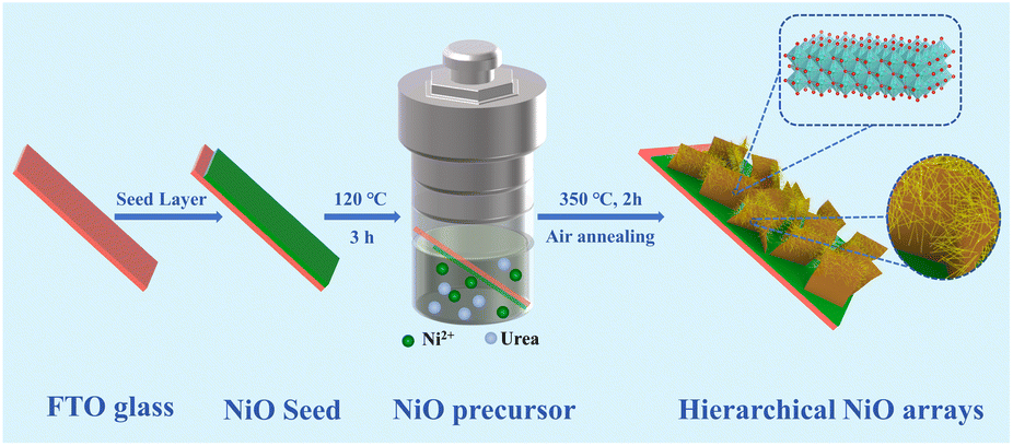 | ||
| Scheme 1 Schematic diagram of the experiment process of hierarchical NiO nanostructures. | ||
Results and discussion
Fig. 1 shows the high-resolution FESEM images of the NiO samples hydrothermally treated for different times. In the initial 1 h reaction, the precursor material exhibits a vertical nanosheet structure on FTO (Fig. 1a). The nanosheet has a length of ∼300 nm, a height of ∼200 nm, and a thickness of ∼20 nm. After reaction for 3 h, a large number of ultrafine nanowires (2–5 nm in diameter) begin to grow on the vertical nanosheets (Fig. 1b and S1a†). The average length is around 145 nm (Fig. S2†). As the reaction time rises to 6 h, more nanowires grow from various parts of the nanosheet, and gradually become longer and begin to interweave (Fig. 1c). With the hydrothermal treatment time further prolonging to 9 h, the upper nanowires become more and even longer to the extent that they cover the nanosheets completely (Fig. 1d). The obtained hierarchical structure possesses an underlying vertical nanosheet structure with a reasonable spacing between the nanosheets and the upper nanowires, which will make more active surface sites exposed and promote charge transfer in the electrolyte to facilitate the electrochemical process. Fig. 1e and f exhibit the TEM and corresponding HRTEM images of NiO-3 h. The crystalline lattice fringes with a distance of 0.204 nm and 0.240 nm can be ascribed to the (200) and (111) planes of cubic NiO, respectively. As shown in Fig. S1b,† these diffraction rings can match well with the (220), (200), and (111) crystal faces. The energy dispersive spectroscopy maps of NiO clearly evidence that Ni and O distribute evenly.11,40,46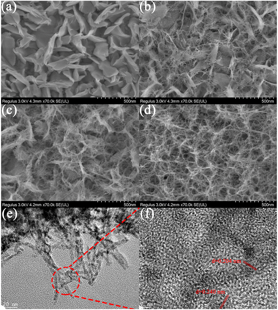 | ||
| Fig. 1 (a–d) High-resolution FESEM images of NiO-1 h, NiO-3 h, NiO-6 h and NiO-9 h. (e) TEM and (f) corresponding HRTEM images of NiO-3 h. | ||
To further understand the growth process of the hierarchical structure, FESEM images of the NiO precursors are shown in Fig. S3,† which show similar morphologies and variation trends to the annealed NiO films, suggesting that the NiO film can well inherit the morphology of the precursor which would not be affected by the post-treatment. Herein, we propose a possible formation mechanism of the unique hierarchical nanostructures as shown in Fig. 2, which can be described as the Ostwald ripening and Oriented attachment process. In the initial stage, plenty of small nucleated particles will start to form in the FTO surface. Simultaneously, when the seed layer is pre-prepared, the surface of the FTO is scattered with many sites of high nickel concentration, which can serve as nucleation sites to form large-sized nanoparticles. According to Yu's work, when the size of nanoparticles exceeds 5 nm, Ostwald ripening can occur where small nucleated particles dissolve and larger particles (seed layer) grow by ingesting the mass of small particles, which minimizes the total interfacial free energy.47 Subsequently, the precursor tends to form a vertical nanosheet structure on the FTO surface. When the nanosheet structure is formed after the nucleation and growth along the seed layer based on the Ostwald ripening mechanism, secondary nucleation would preferentially occur on the surface of the obtained nanosheets due to the depletion of the seed layer. Owing to the fine control of the reactant concentration and reaction parameters, the generated tiny nuclei favor the oriented attachment (OA) growth. The growth mechanism would induce the “one-by-one” connected growth of ultrasmall nuclei to form ultrafine nanowire structure. Simultaneously, secondary nucleation takes place more preferentially on the nanosheet surface than on the substrate surface due to the lower nucleus/particle interfacial energy. The nanosheet can act as a skeleton and also guide the in situ growth of the nanowire. As for the FTO substrate without the seed layer treatment, the nucleation process of the precursors is similar to the above-mentioned secondary nucleation stage. The precursors nucleate on the surface of the untreated FTO and subsequently grow into nanowires without the induction of a seed layer (Fig. S4a†). The cross-sectional SEM images of NiO-9 h show that the upper nanowires and the underlying nanosheets co-exist in the hierarchical structure in Fig. S5.† The morphology evolution observation of the NiO samples with increasing reaction time evidences the above-mentioned two-stage growth mechanism of the hierarchical nanostructures which involves the Ostwald ripening and Oriented attachment stage, respectively.
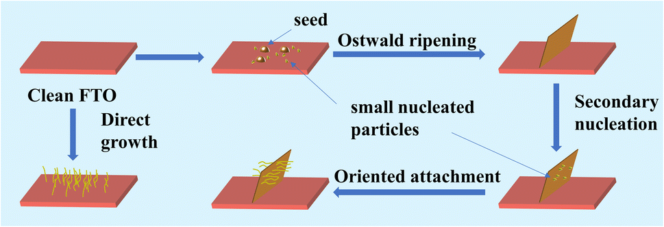 | ||
| Fig. 2 Schematic diagram of the growth mechanism of the NiO hierarchical nanostructures. | ||
In order to determine the suitable annealing temperature before preparation of the NiO thin film, we carried out a TGA test of the precursor powder. The first weight loss from ambient temperature to 260 °C corresponds to adsorbed water on the precursor as shown in Fig. S6.† Then, the Ni precursor will convert to NiO until the temperature reaches 350 °C. It should be noted that NiO which is obtained at this point is not stoichiometric nickel oxide, because the resulting product is still being thermally decomposed for a subsequent period of time until stoichiometric nickel oxide is formed.48,49 Moreover, the resistivity of FTO increases above 350 °C, so we choose this temperature as the optimal annealing temperature. Since the signal of the film was covered by the FTO substrates, all samples were scraped from the substrate to collect the XRD patterns. Fig. 3a exhibits the XRD patterns of synthesized NiO samples which display three prominent diffraction peaks at 37.2°, 43.4°, and 62.8°, indexed to the (111), (200) and (220) planes of cubic NiO (PDF# 47-1049), respectively. No other distinct peaks exist, implying the absence of new impurity phases.50–52 Interestingly, the peak intensity of all NiO samples is high, demonstrating their strong crystallinity. XPS was performed to analyze the surficial compositions and corresponding element states of NiO-3 h. The obtained survey spectrum exhibits the presence of Ni, O and C and absence of other impurities in Fig. 3b. In Fig. 3c, two peaks at binding energies of 853.4 eV and 855.1 eV can represent Ni2+ and Ni3+, respectively. The latter peak possesses a large area, suggesting more Ni3+ content. Ni2+ and Ni3+ co-exist in the NiO-3h film, and since Ni3+ is an electrochromic active factor, more Ni3+ content can help improve the electrochromic performance.22,53 In the O 1s core level, two peaks at 530.7 and 528.8 eV can stand for Ni–O and Ovac, respectively (Fig. 3d). Notably, the peak at about 532.3 eV represents the adsorbed water.25 The electron paramagnetic resonance (EPR) spectrum of the NiO-3 h film is presented in Fig. S7† where a peak corresponding to an EPR signal at g = 2.003 is observed, which stands for existing oxygen vacancies.54–56
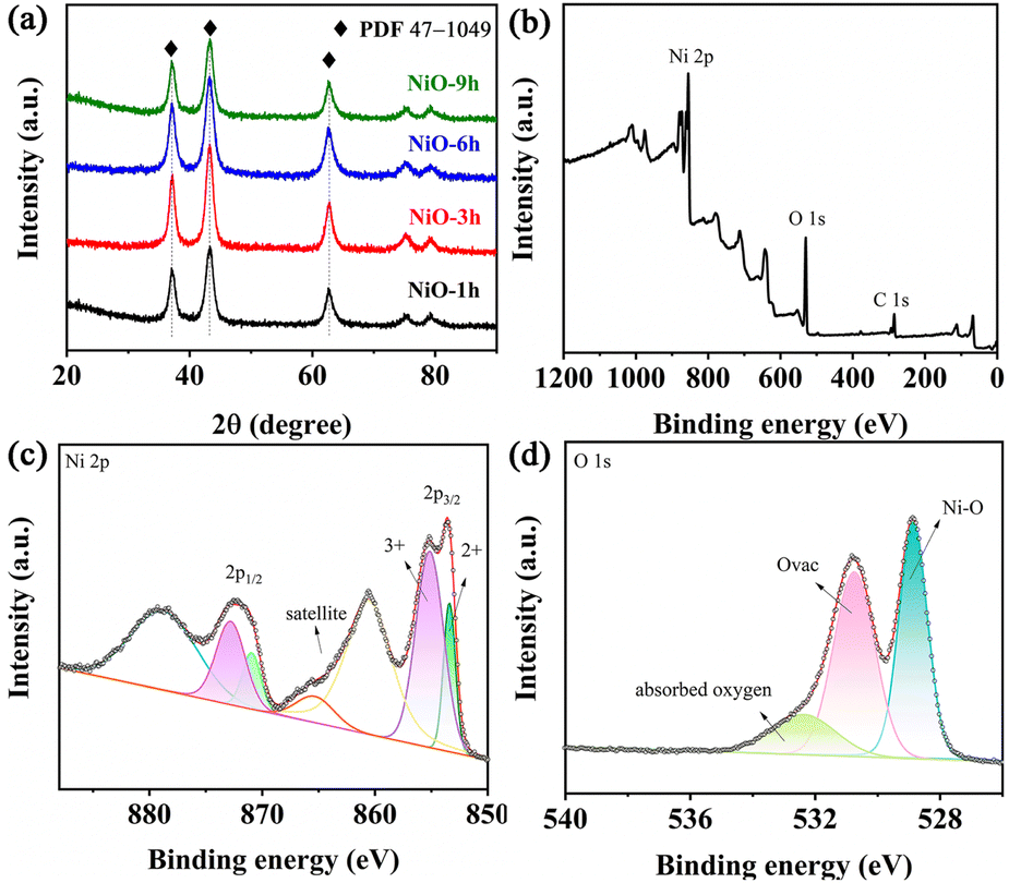 | ||
| Fig. 3 (a) XRD patterns of the NiO samples. (b) XPS full survey spectrum, (c) Ni 2p and (d) O 1s of the NiO-3 h film. | ||
Before the electrochemical tests, an essential activation process was carried out (Fig. S8†). To explore the electrochromic performance of NiO samples, the transmittance spectra of colored and bleached states were investigated (Fig. 4a–d). The NiO-3 h film shows higher transmittance both in visible and NIR regions in the bleached state. Obviously, the transmittance decreases considerably and the sample turns dark brown in the bleached state (Fig. S9†). Optical modulation (ΔT) is a crucial parameter in assessing the electrochromic performance, which means the difference of transmittance at bleached and colored states. Obviously, the NiO-3 h film shows a wide-band color contrast, and the corresponding optical modulation is 95% at 550 nm, compared to 50.8%, 82% and 71.5% for NiO-1 h, NiO-6 h and NiO-9 h, respectively. With increasing reaction time, the optical modulation increases and then decreases, reaching the maximum value at 3 h. Furthermore, it is surprising that NiO-3 h also has a good optical modulation in the NIR region (50.6% at 1000 nm), which is rarely reported for NiO samples in the literature. The introduction of oxygen vacancies may generate an impurity band between the valence band and conduction band in the NiO film, which decreases the band gap and makes the absorption peak shift to the longer wavelength region (red shift), thereby improving the light absorption in the NIR region.57,58 Simultaneously, oxygen vacancies can reduce the energy required for an electron transition to the conduction band, which improves the electronic conductivity and provides better adsorption of oxhydryl for a further redox process, thus improving the electrochromic performance of the material.59–62 According to Fig. S10,† the peak area of Ovac increases with the reaction time, implying a higher oxygen vacancy concentration. However, for electrochromic materials, more oxygen vacancies may lead to the increase of Ni2+ concentration, and decrease of Ni3+ with electrochromic activity, which is harmful to electrochromic performance. The in situ dynamic transmittance spectra were recorded to quantitatively assess the color change feature of the NiO sample as shown in Fig. 4e. The calculated bleaching and coloring times are 5.4 s and 9.8 s, respectively, which are close to those of other NiO films shown in Table S1.†
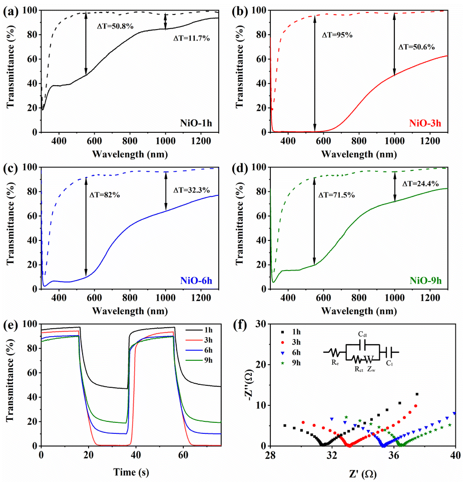 | ||
| Fig. 4 Transmittance spectra of (a) NiO-1 h, (b) NiO-3 h, (c) NiO-6 h and (d) NiO-9 h. (e) Dynamic optical transmittance spectra of the synthesized NiO films. (f) EIS of the NiO films. | ||
To further analyze the charge transport behavior of the obtained NiO samples, electrochemical impedance spectroscopy was performed as shown in Fig. 4f. The inset picture depicts the equivalent circuit, where Rct and Re stand for the charge transfer resistance and electrolyte resistance, respectively. Additionally, Cdl stands for the capacitance of the double capacitive layer. For the linear part, a steeper slope means faster ion diffusion. As shown in Table 1, the calculated Rct of NiO-3 h is 24.53 Ω, implying its low charge transfer impedance. In addition, NiO-3 h has the largest Cdl value of 0.032 μF, indicating the largest electrochemically active area amongst the four samples. It can also be seen that NiO-3 h has the largest slope of the linear part, suggesting a fast mass diffusion. The electrical conductivity of the sample deteriorates with excessive reaction time, which is due to the increasing difficulty of electron diffusion from longer and more dense nanowires to the underlying nanosheets.40,63
| Film | R e (Ω) | C dl (μF) | R ct (Ω) |
|---|---|---|---|
| NiO-1 h | 29.69 | 0.030 | 22.71 |
| NiO-3 h | 30.77 | 0.032 | 24.53 |
| NiO-6 h | 27.58 | 0.027 | 27.20 |
| NiO-9 h | 29.00 | 0.025 | 29.72 |
Coloration efficiency (CE) plays a crucial part in assessing the electrochromic properties which can be evaluated by two formulas.
| CE = ΔOD/Q | (1) |
ΔOD = log![[thin space (1/6-em)]](https://www.rsc.org/images/entities/char_2009.gif) Tb/Tc Tb/Tc | (2) |
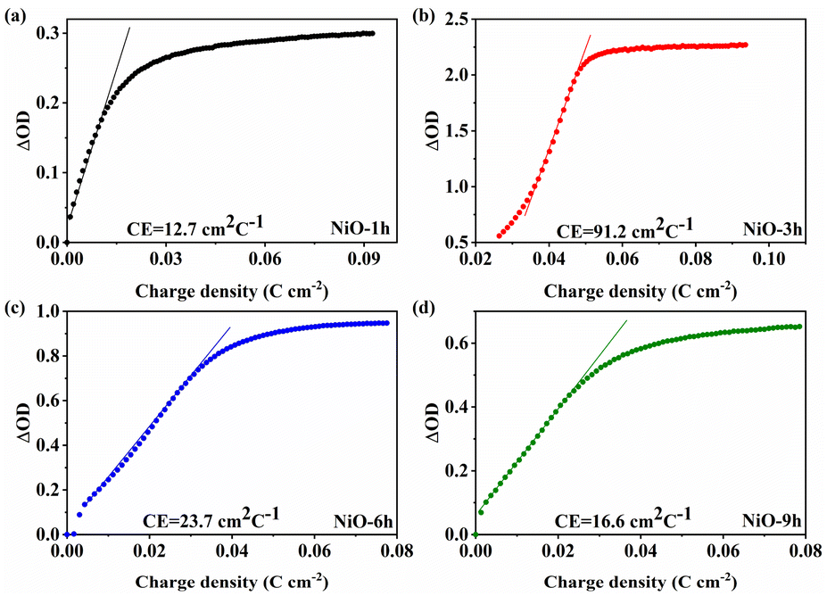 | ||
| Fig. 5 (a–d) The optical density changes with charge density of the NiO films. | ||
CV measurements were performed to assess the charge storage ability. It is obvious that the enclosed area of NiO-3 h is significantly larger than that of the other NiO films as shown in Fig. 6a, indicating that NiO-3 h has a higher electrochemically active area, which coincides with the results from SEM and CE. Meanwhile, with the increase of hydrothermal time, the electrochemically active area of each sample first increased and subsequently decreased, reaching the maximum value at 3 h. Interestingly, such a variation law also applies to the Cdl value of the EIS impedance. Hence, we determine that NiO-3 h has the maximum electrochemically active area. Notably, based on the above analysis, further study of the variation of the active area will help to give a more profound indication of the variation of the electrochemical activity of samples with different morphologies, which will be carried out in future work. Fig. S11† further exhibits the CV curves of NiO-3 h at different scan rates. Two prominent peaks which can be ascribed to the existence of redox reaction of Ni2+ to Ni3+ appear in the films. With the scan rate increasing, both redox peaks show a shift to more positive and negative directions, respectively. Notably, the shape of the CV curves basically remains unchanged, implying outstanding electrochemical reversibility. The reversible redox process can also provide potential super-capacitive performance. In addition, the diffusion and pseudocapacitance control processes can be identified due to the following relation:
| logi = b × logν + loga | (3) |
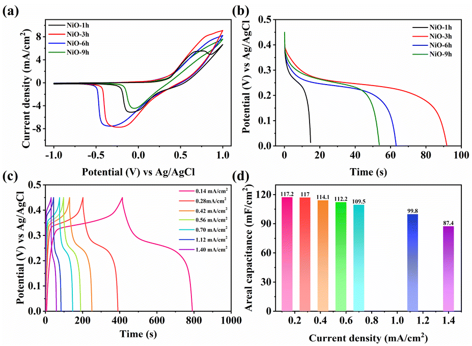 | ||
| Fig. 6 (a) CV curves at a scan rate of 0.005 V s−1 and (b) galvanostatic discharge curves of the synthesized NiO films. (c) Galvanostatic charge/discharge curves and (d) corresponding calculated areal capacitance of NiO-3 h at different current densities. | ||
Fig. 6c shows that the charge–discharge curves are symmetrical, meaning good reversibility, consistent with CV analysis. NiO-3 h possesses the highest areal capacitance performance (117.2 mF cm−2 at 0.14 mA cm−2). The areal capacitance can still remain at 74.6% even when increasing the current density to tenfold, exhibiting optimal rate capability of the hierarchical nanofilm (Fig. 6d). Notably, the GCD curve demonstrates that the NiO-3 h film exhibits distinct characteristics of a battery-type supercapacitor. Unlike the classical double-layer supercapacitor, two distinct plateaus appear when charging and discharging, representing the generation of redox processes accompanying the phase transition process, that is, Ni2+/Ni3+ redox processes. The battery-type supercapacitor feature based on the electrochemical redox process contributes to the enhanced super-capacitance performance and may find promising potential for electrochromic energy storage. Repetitive charge/discharge measurements were performed at 0.42 mA cm−2 for 1000 cycles to assess their cycle performance. Fig. S13† shows that the NiO-3 h electrode retained 58.5% of its initial capacitance. The sample loses 39% of its initial value after the first 700 cycles but only an additional 2.5% is lost in the next 300 cycles. Nevertheless, the sample maintains a high coulombic efficiency of 97%. This is ascribed to the robust hierarchical arrays of the electrodes, which contribute to the ion movement in electrolyte.44,66,67
As for electrochromic application, long-term cycling stability is also a crucial part to assess the durability of the material. In Fig. 7a, NiO-3 h was cycled for 700 times between −1.0 V and +1.0 V using chronoamperometry measurements. During cycling, the injection/extraction current of the film decreases slightly. Meanwhile, the optical modulation of the films maintains a retention of 88.1% after 500 cycles and 82.2% after 700 cycles as shown in Fig. 7b, which has been considerably improved in comparison with previous reports. To investigate the material state after cycling, we performed CV tests for each cycle number in Fig. 7c. The enclosed area and observed peak current of the CV curve gradually decrease with increasing number of cycles, implying a decrease in electrochemical activity. In summary, NiO-3 h shows advanced electrochromic energy storage performance in comparison with previous reports. The detailed data of some reported NiO films are listed in Table S2.†
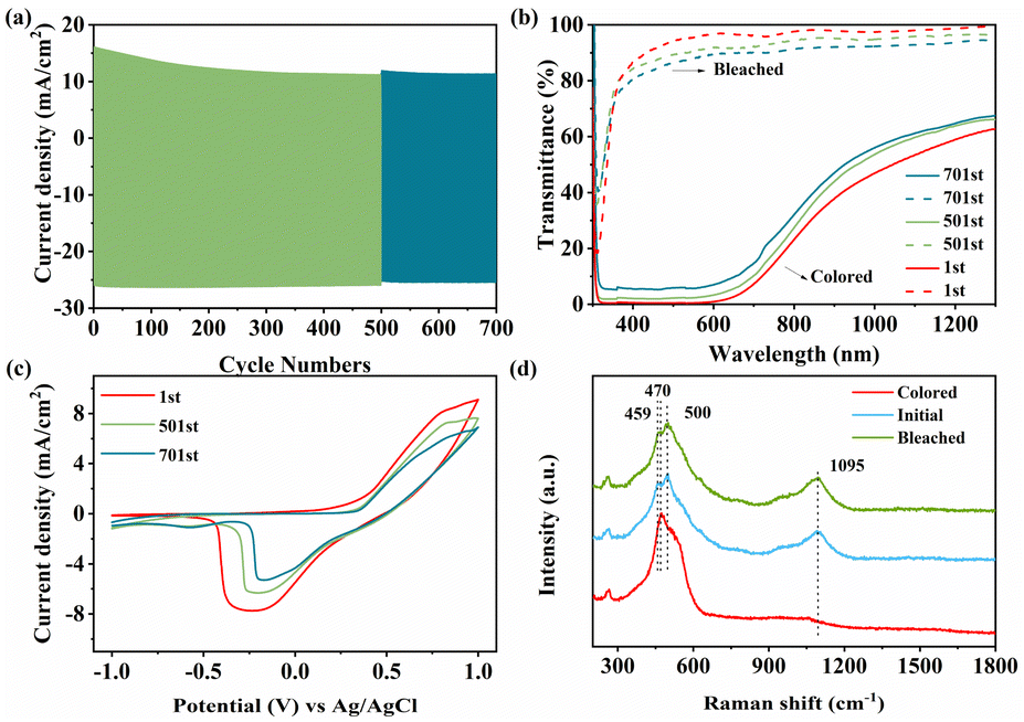 | ||
| Fig. 7 (a) Current data of NiO-3 h before and after 700 cycles at 550 nm. (b) Transmittance spectra and (c) CV curves of NiO-3 h before and after 700 cycles. (d) Raman spectra of the initial state, bleached and colored state for the NiO-3 h sample. | ||
The exact mechanism of electrochromism in NiO in alkaline environments is still controversial, but it is well accepted that phase change due to the reversible conversion of Ni2+ to Ni3+ is a key factor. Therefore, Raman tests were carried out on the films in the initial, colored and bleached states as shown in Fig. 7d. For the initial state, the peak at 1095 cm−1 can stand for the 2LO phonon modes of NiO.68 When the film is in the coloring state, the peaks of NiO disappear, while a peak at 470 cm−1 which can stand for the stretching vibration of the Ni–O–OH bond arises. The result shows that NiO is oxidized to NiOOH during the coloring process. Moreover, the bleached film shows two peaks at 459 and 500 cm−1 referring to the A1g stretching modes in Ni(OH)2. Raman measurements were further performed on the samples after 700 cycles, as shown in Fig. S14a.† The characteristic spectrum of the colored film exhibits two peaks at 474 and 557 cm−1 attributed to the eg bending vibration and A1g stretching vibrational modes in NiOOH, respectively.69–71 Compared to the uncycled colored state film, the peak of the cycled film is sharper and a characteristic peak located at 550 cm−1 appears, indicating an increased NiOOH concentration. Moreover, in the bleached state, the broad peak at 1095 cm−1 is lower in intensity than that of the initial bleached film, implying a lower amount of NiO. The peak at 500 cm−1 refers to Ni(OH)2, which is prominent after 700 cycles. Simultaneously, the observed cycled XPS peak shifts toward higher binding energy, suggesting the formation of new higher valence Ni ions (Fig. S14b†). Based on the discussion above, the electrochromic mechanism of the NiO film can be concisely summarized as two steps:
| NiO + OH− → NiOOH + e− | (4) |
| NiOOH + H2O ↔ Ni(OH)2 + OH− | (5) |
In the beginning of the coloring and bleaching cycle, the electrochromic reaction of the film is dominated by reaction (4), in which OH− is injected into the film and combines with NiO to form NiOOH to release an electron under positive bias. Then, NiOOH generated in the coloring process is gradually converted to Ni(OH)2 in the bleaching process during the cycling, so that the amount of Ni(OH)2 increases, i.e., reaction (5) occurs. This also means that NiO is gradually converted to NiOOH during the whole cycling process, and the subsequent electrochromic process is achieved by the interconversion of transparent Ni(OH)2 and dark brown NiOOH. The conversion of NiO to NiOOH is not completely reversible. NiOOH belongs to the hexagonal crystal lattice while NiO has a cubic crystal structure. Therefore, the cycling process will lead to the electrochromic degradation of the NiO films due to the mismatch in the crystal phase.
The optimized electrochromic and energy storage properties can be ascribed to the unique NiO nanosheet/nanowire hierarchical structure.72–74 First, the pre-seed layer can induce the precursor to form the primary nanosheet structure, which can provide good mechanical bonding and improve charge transport between the electrochromic structure and the FTO glass. Second, compared with NiO-1 h, NiO-3 h possesses newly generated nanowires with more active sites involved in the electrochemical reaction, and the newly formed hierarchical nanostructures prompt the nanosheets and nanowires to be completely exposed to the electrolyte, thus enhancing the diffusion of ions as well as the penetration of the electrolyte for efficient utilization of the active sites. However, with the prolongation of hydrothermal time, nanowires become longer and tend to bunch up together, which would hinder the electrolyte penetration and ion exchange. The charge transport path from upper nanowires to underlying nanosheets also becomes longer, resulting in lower electrical conductivity. Therefore, too long reaction time would cause longer and crowder nanowires, deteriorating the electrochromic and electrocapacitive performance. Finally, the underlying nanosheets are interconnected to form a sheet-like network. These nanosheets support each other to form a stable structure. Moreover, the nanowires growing at the edges of the nanosheets are extremely thin and long, which allows sufficient three-dimensional space to mitigate volume expansion and structural disruption by the phase change due to ion injection/extraction during cycling, thus improving the long-term cycling properties.
Conclusions
In summary, hierarchical NiO nanosheet@nanowire films were prepared by a one-step hydrothermal method and subsequent heat treatment process. The morphology evolution observation evidences a two-stage growth mechanism which involves Ostwald ripening and an oriented attachment stage. The NiO film exhibits excellent electrochromic properties, superior color contrast in the visible and NIR region, quick color change, improved coloration efficiency, and optimal long-term cycling properties. Additionally, the unique hierarchical nanostructures possess high super-capacitive properties. The excellent electrochemical properties are ascribed to the pre-treated seed layer and unique three-dimensional hierarchical structure of underlying nanosheets and upper nanowires, which expose more active area, facilitate charge transfer and mass diffusion, and contribute to improved cycling stability. This work will inspire a development of using a facile and low-cost technique to fabricate hierarchical nanostructures for efficient electrochromic energy storage applications.Conflicts of interest
There are no conflicts to declare.Acknowledgements
This project is supported by the National Natural Science Foundation of China (Grant No. 52072106, U1810204, 52172293, and 51972093), the Key R&D Projects of Anhui Province (202104b11020016), Natural Science Foundation of Anhui Province (2108085MB45), Fundamental Research Funds for the Central Universities (PA2021KCPY0044, PA2021GDSK0088, and PA2021GDSK0094), and the Higher Education Discipline Innovation Project “New Materials and Technology for Clean Energy” (B18018).References
- Y. Huang, B. Wang, F. Chen, Y. Han, W. Zhang, X. Wu, R. Li, Q. Jiang, X. Jia and R. Zhang, Adv. Opt. Mater., 2021, 10, 2101783 CrossRef.
- X. Li, K. Perera, J. He, A. Gumyusenge and J. Mei, J. Mater. Chem. C, 2019, 7, 12761–12789 RSC.
- A. Llordes, G. Garcia, J. Gazquez and D. J. Milliron, Nature, 2013, 500, 323–326 CrossRef CAS PubMed.
- G. A. Niklasson and C. G. Granqvist, J. Mater. Chem., 2007, 17, 127–156 RSC.
- J. Wang, X. Huo, M. Guo and M. Zhang, J. Energy Storage, 2022, 47, 103597 CrossRef.
- T. Y. Yun, X. Li, S. H. Kim and H. C. Moon, ACS Appl. Mater. Interfaces, 2018, 10, 43993–43999 CrossRef CAS PubMed.
- G. Cai, X. Wang, M. Cui, P. Darmawan, J. Wang, A. L.-S. Eh and P. S. Lee, Nano Energy, 2015, 12, 258–267 CAS.
- J. Guo, M. Wang, G. Dong, Z. Zhang, Q. Zhang, H. Yu, Y. Xiao, Q. Liu, J. Liu and X. Diao, Inorg. Chem., 2018, 57, 8874–8880 CrossRef CAS PubMed.
- J. Mao, X. Duan and A. Yao, Aust. J. Chem., 2019, 72, 957–963 CrossRef CAS.
- I. Saadeddin, M. Suleiman, H. Salman, K. Zrikem, G. Song and A. Rougier, Solid State Ionics, 2019, 343, 115129 CrossRef CAS.
- J. Shi, L. Lai, P. Zhang, H. Li, Y. Qin, Y. Gao, L. Luo and J. Lu, J. Solid State Chem., 2016, 241, 1–8 CrossRef CAS.
- C. Wu, Y. Yang, W. Feng, W. Song and R. Tan, J. Alloys Compd., 2021, 862, 158665 CrossRef CAS.
- S. Balasubramaniam, A. Mohanty, S. K. Balasingam, S. J. Kim and A. Ramadoss, Nano-Micro Lett., 2020, 12, 85 CrossRef CAS PubMed.
- T. S. Mathis, N. Kurra, X. Wang, D. Pinto, P. Simon and Y. Gogotsi, Adv. Energy Mater., 2019, 9, 1902007 CrossRef CAS.
- J. Zhou, S. Zhang, Y.-N. Zhou, W. Tang, J. Yang, C. Peng and Z. Guo, Electrochem. Energy Rev., 2021, 4, 219–248 CrossRef CAS.
- Y. Jiang, F. Guo, Y. Liu, Z. Xu and C. Gao, SusMat, 2021, 1, 304–323 Search PubMed.
- M. Kang, H. Zhou, P. Wen and N. Zhao, ACS Appl. Energ. Mater., 2021, 4, 1619–1627 CrossRef CAS.
- X. Luo, S. Chen, T. Hu, Y. Chen and F. Li, SusMat, 2021, 1, 211–240 CrossRef.
- M. Rastgoo-Deylami and A. Esfandiar, ACS Appl. Energy Mater., 2021, 4, 2377–2387 CrossRef CAS.
- Z. Xu, W. Deng and X. Wang, Electrochem. Energy Rev., 2021, 4, 269–335 CrossRef CAS.
- G. Cai, J. Chen, J. Xiong, A. Lee-Sie Eh, J. Wang, M. Higuchi and P. S. Lee, ACS Energy Lett., 2020, 5, 1159–1166 CrossRef CAS.
- X. Guo, X. Diao and W. Wang, Ceram. Int., 2021, 47, 22240–22245 CrossRef CAS.
- Z. Luo, L. Liu, X. Yang, X. Luo, P. Bi, Z. Fu, A. Pang, W. Li and Y. Yi, ACS Appl. Mater. Interfaces, 2020, 12, 39098–39107 CrossRef CAS PubMed.
- S. Xie, Y. Chen, Z. Bi, S. Jia, X. Guo, X. Gao and X. Li, Chem. Eng. J., 2019, 370, 1459–1466 CrossRef.
- H. Zhang, S. Liu, T. Xu, W. Xie, G. Chen, L. Liang, J. Gao and H. Cao, J. Mater. Chem. C, 2021, 9, 17427–17436 RSC.
- Z. Li, Z. Yu, W. Wang, J. Hou, L. Gao, X. Gu and G. Su, Mater. Chem. Phys., 2021, 269, 124738 CrossRef CAS.
- D. Ma, G. Shi, H. Wang, Q. Zhang and Y. Li, Nanoscale, 2013, 5, 4808–4815 RSC.
- S. A. Mozaffari, S. H. Mahmoudi Najafi and Z. Norouzi, Electrochim. Acta, 2021, 368, 137633 CrossRef CAS.
- L. Zhu, C. K. Nuo Peh, T. Zhu, Y.-F. Lim and G. W. Ho, J. Mater. Chem. A, 2017, 5, 8343–8351 RSC.
- W. Zhu, Z. Lu, G. Zhang, X. Lei, Z. Chang, J. Liu and X. Sun, J. Mater. Chem. A, 2013, 1, 8327–8331 RSC.
- S. I. Kim, J. S. Lee, H. J. Ahn, H. K. Song and J. H. Jang, ACS Appl. Mater. Interfaces, 2013, 5, 1596–1603 CrossRef CAS PubMed.
- Q. Yang, Z. Lu, Z. Chang, W. Zhu, J. Sun, J. Liu, X. Sun and X. Duan, RSC Adv., 2012, 2, 1663–1668 RSC.
- X. Y. Liu, Y. Q. Zhang, X. H. Xia, S. J. Shi, Y. Lu, X. L. Wang, C. D. Gu and J. P. Tu, J. Power Sources, 2013, 239, 157–163 CrossRef CAS.
- J. Xue, H. Xu, S. Wang, T. Hao, Y. Yang, X. Zhang, Y. Song, Y. Li and J. Zhao, Appl. Surf. Sci., 2021, 565, 150512 CrossRef CAS.
- W. Chen, J. Wang, K. Y. Ma, M. Li, S. H. Guo, F. Liu and J. P. Cheng, Appl. Surf. Sci., 2018, 451, 280–288 CrossRef CAS.
- J. Liu, C. Cheng, W. Zhou, H. Li and H. J. Fan, Chem. Commun., 2011, 47, 3436–3438 RSC.
- Y. Mao, Y. Cheng, J. Wang, H. Yang, M. Li, J. Chen, M. Chao, Y. Tong and E. Liang, New J. Chem., 2016, 40, 107–112 RSC.
- X. Wang, B. Liu, J. Tang, G. Dai, B. Dong, L. Cao, R. Gao and G. Su, Sol. Energy Mater. Sol. Cells, 2019, 191, 108–116 CrossRef CAS.
- S.-W. Zhang, B.-S. Yin, C. Liu, Z.-B. Wang and D.-M. Gu, Chem. Eng. J., 2017, 312, 296–305 CrossRef CAS.
- J. Xue, W. Li, Y. Song, Y. Li and J. Zhao, J. Alloys Compd., 2021, 857, 158087 CrossRef CAS.
- Y. Ren, X. Zhou, H. Zhang, L. Lei and G. Zhao, J. Mater. Chem. C, 2018, 6, 4952–4958 RSC.
- K.-H. Kim, S.-J. Jeong, B.-R. Koo and H.-J. Ahn, Appl. Surf. Sci., 2021, 537, 147902 CrossRef CAS.
- Y. He, T. Li, X. Zhong, M. Zhou, G. Dong and X. Diao, Electrochim. Acta, 2019, 316, 143–151 CrossRef CAS.
- F. Khan, Surfaces and Interfaces, 2022, 29, 101792 CrossRef CAS.
- A. Dewan, S. Haldar and R. Narayanan, J. Solid State Electrochem., 2020, 25, 821–830 CrossRef.
- Y. Wei, F. Yan, X. Tang, Y. Luo, M. Zhang, W. Wei and L. Chen, ACS Appl. Mater. Interfaces, 2015, 7, 21703–21711 CrossRef CAS PubMed.
- X. Chen, J. Wan, J. Wang, Q. Zhang, L. Gu, L. Zheng, N. Wang and R. Yu, Adv. Mater., 2021, 33, 2104764 CrossRef CAS PubMed.
- D. Wang, R. Xu, X. Wang and Y. Li, Nanotechnology, 2006, 17, 979–983 CrossRef CAS PubMed.
- X. H. Xia, J. P. Tu, J. Zhang, X. L. Wang, W. K. Zhang and H. Huang, Sol. Energy Mater. Sol. Cells, 2008, 92, 628–633 CrossRef CAS.
- A. Dewan, S. Sur, R. Narayanan and M. O. Thotiyl, ChemElectroChem, 2022, 9, e202200001 CrossRef CAS.
- K. Song, L. Yuan, Z. Liu, H. Qiao, Y. Yu, X. Shen and X. Hu, New J. Chem., 2022, 46, 1601–1607 RSC.
- X. Xia, Z. Ku, D. Zhou, Y. Zhong, Y. Zhang, Y. Wang, M. J. Huang, J. Tu and H. J. Fan, Mater. Horizons, 2016, 3, 588–595 RSC.
- H. Wang, B. Fan, Z. Luo, Q. Wu, X. Zhou and F. Wang, Catal. Sci. Technol., 2021, 11, 7632–7639 RSC.
- S. Luo, X. Li, W. Gao, H. Zhang and M. Luo, Sustainable Energy Fuels, 2020, 4, 164–170 RSC.
- S. Visweswaran, R. Venkatachalapathy, M. Haris and R. Murugesan, Appl. Phys. A, 2020, 126, 524 CrossRef CAS.
- J. Zheng, Y. Lyu, C. Xie, R. Wang, L. Tao, H. Wu, H. Zhou, S. Jiang and S. Wang, Adv. Mater., 2018, 30, 1801773 CrossRef PubMed.
- D. Kong, J. Qi, D. Liu, X. Zhang, L. Pan and J. Zou, Trans. Tianjin Univ., 2019, 25, 340–347 CrossRef CAS.
- H. Liu, F. Zeng, Y. Lin, G. Wang and F. Pan, Appl. Phys. Lett., 2013, 102, 181908 CrossRef.
- J. H. Lin, Y. T. Yan, T. X. Xu, C. Q. Qu, J. Li, J. Cao, J. C. Feng and J. L. Qi, J. Colloid Interface Sci., 2020, 560, 34–39 CrossRef CAS PubMed.
- H. Sun, Y. Zhao, K. Molhave, M. Zhang and J. Zhang, Nanoscale, 2017, 9, 14431–14441 RSC.
- Z. Xiao, Y. Wang, Y.-C. Huang, Z. Wei, C.-L. Dong, J. Ma, S. Shen, Y. Li and S. Wang, Energy Environ. Sci., 2017, 10, 2563–2569 RSC.
- D. Yan, W. Wang, X. Luo, C. Chen, Y. Zeng and Z. Zhu, Chem. Eng. J., 2018, 334, 864–872 CrossRef CAS.
- C. Su, M. Qiu, Y. An, S. Sun, C. Zhao and W. Mai, J. Mater. Chem. C, 2020, 8, 3010–3016 RSC.
- P. Lei, J. Wang, P. Zhang, S. Liu, S. Zhang, Y. Gao, J. Tu and G. Cai, J. Mater. Chem. C, 2021, 9, 14378–14387 RSC.
- D. Ma, G. Shi, H. Wang, Q. Zhang and Y. Li, J. Mater. Chem. A, 2013, 1, 684–691 RSC.
- X. Huo, R. Li, J. Wang, M. Zhang and M. Guo, Chem. Eng. J., 2022, 430, 132821 CrossRef CAS.
- T. Wang, H. C. Chen, F. Yu, X. S. Zhao and H. Wang, Energy Storage Mater., 2019, 16, 545–573 CrossRef.
- Y. Li, L. Hu, W. Zheng, X. Peng, M. Liu, P. K. Chu and L. Y. S. Lee, Nano Energy, 2018, 52, 360–368 CrossRef CAS.
- O. Diaz-Morales, D. Ferrus-Suspedra and M. T. M. Koper, Chem. Sci., 2016, 7, 2639–2645 RSC.
- S. Klaus, Y. Cai, M. W. Louie, L. Trotochaud and A. T. Bell, J. Phys. Chem. C, 2015, 119, 7243–7254 CrossRef CAS.
- S. Yao, H. Wei, Y. Zhang, X. Zhang, Y. Wang, J. Liu, H. H. Tan, T. Xie and Y. Wu, Catal. Sci. Technol., 2021, 11, 264–271 RSC.
- F. Li, M. Huang, J. Wang, J. Qu, Y. Li, L. Liu, V. K. Bandari, Y. Hong, B. Sun, M. Zhu, F. Zhu, Y. X. Zhang and O. G. Schmidt, Energy Storage Mater., 2020, 27, 17–24 CrossRef.
- T. Wang, Y. Wang, J. Lei, K. J. Chen and H. Wang, Exploration, 2021, 1, 20210178 CrossRef.
- X. Zhao, X. Liu, F. Li and M. Huang, J. Mater. Sci., 2019, 55, 2482–2491 CrossRef.
Footnote |
| † Electronic supplementary information (ESI) available. See https://doi.org/10.1039/d2na00505k |
| This journal is © The Royal Society of Chemistry 2022 |