
Actual origin and precise control of asymmetrical hysteresis in an individual CH3NH3PbI3 micro/nanowire for optical memory and logic operation
Runna
Gou
a,
Zhiyong
Ouyang
b,
Changsen
Xu
b,
Song
He
a,
Shouduan
Cheng
a,
Cencen
Shi
b,
Jie
Zhao
a,
Yanhe
Xiao
a,
Shuijin
Lei
 a and
Baochang
Cheng
*ab
a and
Baochang
Cheng
*ab
aSchool of Physics and Materials, Nanchang University, Jiangxi 330031, P. R. China. E-mail: bcheng@vip.sina.com
bNanoscale Science and Technology Laboratory, Institute for Advanced Study, Nanchang University, Jiangxi 330031, P. R. China
First published on 22nd July 2022
Abstract
Although CH3NH3PbI3 can present an excellent photoresponse to visible light, its application in solar cells and photodetectors is seriously hindered due to hysteresis behaviour. Moreover, for its origin, there exist different opinions. Herein, we demonstrate a route to realize precise control for the electrical transport of a single CH3NH3PbI3 micro/nanowire by constructing a two-terminal device with asymmetric Ag and C electrodes, and its hysteresis can be clearly identified as a synergistic effect of the redox reaction at the interface of the Ag electrode and the injection and ejection of holes in the interfacial traps of the C electrode rather than its bulk effect. The device can show superior bias amplitude and illumination intensity dependence of hysteresis loops with typical bipolar resistive switching features. Thus, an excellent multilevel nonvolatile optical memory can be effectively realized by the modulation of the illumination and bias, and moreover a logic OR gate operation can be successfully implemented with voltage and illumination as input signals as well. This work clearly reveals and provides a new insight of hysteresis origin that can be attributed to a synergistic effect of two asymmetrical electrode interfaces, and therefore precisely controlling its electrical transport to realize an outstanding application potential in multifunctional devices integrated with optical nonvolatile memory and logic OR gate operation.
New conceptsFor CH3NH3PbI3-based devices, their current–voltage curves generally exhibit hysteresis behaviour, which affects seriously device performance. Moreover, the resistive switching effect is considered to come from the formation and rupture of conductive filaments, but it is still controversial. To reveal the true origin and realize controllable modulation, a single CH3NH3PbI3 micro/nanowire was selected to construct a two-terminal device with asymmetric Ag and C electrodes. When a relatively large positive voltage is applied to the Ag electrode, Ag is easily oxidized to Ag+ and then reacts with I− to form AgIx, resulting in the height decrease and width increase of the interface barrier, and contrarily, an inverse reaction occurs when a large reverse voltage is applied. Meanwhile, for the C electrode, the redox reaction hardly occurs, and when a large positive voltage is applied, holes are effectively injected into interfacial traps, thereby decreasing both the height and width of the interface barrier. Conversely, when applying a large reverse voltage, the holes are ejected, correspondingly increasing the height and width of the interface barrier. This study clearly reveals that the hysteresis actually originates from the electrode interface effect, and thus nonvolatile multilevel memory and adjustable logic operation can be well implemented by a synergism of illumination and bias. |
1. Introduction
With the explosive growth of big data, the requirements for information storage speed and capacity are getting higher and higher. Based on the modern computer architecture described by von Neumann, there exist huge data transmission delays and lag in running speeds due to the differences of separation modes between memory and processor operation, which not only leads to an increase in the amount of energy consumption, but also the decrease of the operating efficiency during data transmission.1 Brain-like operation has shown great advantages of high operating speed, low energy loss and certain fault tolerance in complex learning, recognition and storage.2 Inspired by this, it is of great significance to construct an individual device integrated with both memory and a processor, which can synchronously store and process the information like the human brain, and meanwhile significantly reduce the energy consumption, speed up the operating of computer chips, and further accelerate the maturation of deep learning concepts.3–6 Compared with the traditional complementary oxide semiconductor logic circuit, the two-terminal memristors based on multifunctional photoelectric storage devices have the advantages of easy integration and low energy consumption due to their simple structure, low switching voltage, high storage density, fast operating speed, and low energy loss. They can directly process and store the optical and electrical signals, and moreover can be expected to synchronously realize the logic OR gate operations and information storage with fewer storage units, so as to overcome the von Neumann bottleneck.7–9Memristors, as the fourth kind of passive basic circuit element, are a kind of nonlinear resistor with charge memory function, which can present a characteristic hysteresis loop under the stimulation of external periodic electrical signals, and then realize the storage function of 0/1 information with the advantages of high speed, low power consumption, easy integration, simple construction, and compatibility with CMOS technology; therefore, not only can the performance requirements of next-generation high-density information storage and high-performance computing for general-purpose electronic memory be well fulfilled, but also the nonvolatile state logic operation and brain-like neural morphology calculation can be expected to be realized.10–13 Chen et al. fabricated a van der Waals heterojunction by selecting two-dimensional materials with suitable energy bands, and successfully simulated various functions of synapses, such as EPSC/IPSC, PPF, SRDP, and LTP/LDP.14 At present, most researches are focused on the two-terminal resistive switching memories (RRAM), which can realize information storage and operation through the reversible transition between a high resistance state (HRS) and low resistance state (LRS).
However, the physical mechanism is still full of disputes; generally, it can be concluded as the formation and rupture of conductive filaments, the lattice distortion caused by the phase transition, and the capture/decapture of charge.15–18 In recent years, to improve the performance of RRAM, large amounts of research have been carried out on nanoparticles, binary metal oxides, organic materials, graphene, and even perovskite materials as the storage medium. For instance, the research of ABX3 type perovskite materials such as BaTiO3, SrRuO3, SrZrO3 and other solid-state ceramic materials with single or multiple structures in RRAM has been widely reported,19,20 such that the SrTiO3, SrZrO3:Cr, and hybrid perovskite materials,21 and their multilevel adjustable resistive state, bipolar resistive switching (RS) properties and different resistive storage behaviours induced by light, temperature or a magnetic field have been revealed for the first time.
As one of the most widely studied perovskite semiconductor materials in recent years, CH3NH3PbI3 organic–inorganic hybrid perovskite, which has a unique electronic energy band structure, excellent photoelectric properties, an adjustable direct band gap of ∼1.55 eV, high carrier mobility, high absorption coefficient, and long carrier diffusion length,22 has aroused extensive research interest in various devices such as solar cells and light-emitting diodes.23 In addition, the special crystal ABX3 type structure of CH3NH3PbI3 makes its defect tolerance excellent. Recent investigations have shown that not only the migration activation energy of I− (0.1–0.6 eV) and MA+ (0.5–0.8 eV) in CH3NH3PbI3 perovskite, but also the formation energy of other possible point defects, including vacancies (VPb, VMA, and VI), interstitial defects (Pbi, MAi, and Ii), and anti-position defects (PbI, IPb), which can form a series of defects with various energy levels, and then capture charges, are very low.24 The most likely reason can be attributed to the inevitable formation of shallow or deep defects during the process of organic–inorganic hybrid perovskite crystals, which finally strongly affect the performance of the device, such as the hysteresis loop,25 non-radiative recombination,26 charge capture,27 charge scattering,28 and ion migration.29 Considering the special operating mechanism of defects in the process of charge capture and migration, CH3NH3PbI3-based RS memory has an outstanding application potential. For example, the bipolar RS device, based on a structure of Au/perovskite/FTO manufactured by Yoo et al. shows stable durability and long nonvolatile performance.22 The RS is realized by a capture and decapture modulation of traps (defects), which leads to different conductive states, such as ohmic conduction, trap-controlled space charge limit current, or Poole–Frenkel conduction. Choi et al. realized an ultra-low voltage multilevel RS device with high on/off ratio by using a structure of Ag/perovskite/Pt,30 which can be attributed to the low activation energy of I− ion migration. However, the perovskite memristors with a current–voltage (I–V) hysteresis effect are usually prepared with perovskite oxides, such as SrRuO3,31 SrTiO3,32 and CH3NH3PbI3,33 whose on/off ratio of currents can hardly exceed 4 orders of magnitude. The ITO/CH3NH3PbI3/MoO3/Ag nonvolatile memory device prepared by Zhou et al.34 and Au/MAPbI3/Au monopole resistance memory devices constructed by Keehoon et al.35 can achieve good nonvolatile storage characteristics, high ON/OFF ratio, and long hold time. The ON/OFF ratio of Au/MAPbI3/Au monopole resistance memory devices can reach 108. In addition, multifunctional perovskite quantum dots floating gates (PQDs-FGs) transistors, fabricated by Ding et al., can realize multilevel photoelectric logic computing and in situ memory simultaneously in a single device.36 Floating gate organic field effect transistors (FGOFETM), prepared with perovskite quantum dots embedded in a polystyrene matrix by Li et al. can realize multilevel data storage under electrical programming and photo induced-reset processes. The eminent overall memory performance, excellent multilevel storage and good reliability with the retention time over 10 years show a huge potential.37 Waseem raja et al. achieved excellent conversion efficiency surpassing the efficiency of single junction perovskite and c-Si solar cells by using nanocolumnar (NP) array-based perovskite/carbon–silicon tandem solar cells.38 These studies fully demonstrate the potential of perovskite materials in storage, neuromorphic computing, artificial intelligence, and information security.39 On the other hand, perovskite devices with excellent performance are expected to achieve long-term stability if they can be treated with encapsulation technology to isolate water and oxygen.40,41 Therefore, making full use of the good photoelectric properties and special memory resistance properties of halide perovskite materials, and then further optimizing them is of great significance for their wide application.
One-dimensional (1D) nanostructured semiconductors, such as nanowires and nanorods, have many advantages over other materials; not only are the preparation method and structure very simple, but also surface states are very rich due to the large numbers of dangling bonds caused by a termination of lattice periodic symmetry on the surface.42–44 Additionally, the properties of 1D nanostructured semiconductors are much easier to control on the nanoscale, forming lots of special properties that are far different from their bulk materials, and making them good candidates for optoelectronic devices. Therefore, it is easier to explore the origin of the RS effect and realize corresponding high-performance devices from the 1D nanostructure-based devices.45–48 Herein, 1D CH3NH3PbI3 micro/nanowires were synthesized by a two-step low-temperature annealing method, and then a single micro/nanowire based asymmetric two-terminal device with a structure of Ag/CH3NH3PbI3/C was constructed on an insulating Kapton substrate. Then, the I–V hysteresis was systematically studied by applying different bias voltages and illuminating different regions with various intensities of VIS. The origin of the hysteresis behavior is deeply discussed and precisely identified. After being modulated with large bias and strong illumination, the device can show a superior photoresponse. Moreover, by illuminating different regions and loading different biases to the device, the precise control of the I–V characteristics with different hysteresis behavior can be implemented. Thus, multilevel optical nonvolatile memory can be obtained, and meanwhile by utilizing the difference of photoresponse under different resistance states, the electric field and illumination can be used as the input sources to achieve the logic operation of a single device. By systematic microregion photoresponse research on a 1D nanostructure-based two-terminal device, the behaviour can be identified as the bias- and illumination-induced synergistic effect of the interface barrier height and width variation related to the redox reaction of Ag ↔ Ag+ at the interface of the Ag electrode and the injection and ejection of holes in the interfacial traps of the C electrode. After only being applied with a relatively large opposite voltage, the device can show a clockwise hysteresis along the Ag electrode direction, and conversely it can show a counterclockwise hysteresis loop along the C electrode direction. By appropriate device design and precise external regulation, the nanostructured CH3NH3PbI3 perovskite can show excellent application potential in the integration of optical nonvolatile memory and logic operation. Our work provides a potential application strategy for the development of multifunctional integrated devices in the fields of logic circuits, optical digital computing, and optical quantum information.
2. Experimental
2.1 Synthesis of CH3NH3PbI3 micro/nanowires
CH3NH3PbI3 micro/nanowires were prepared via a fast liquid–solid growth method of supersaturated solution with the evaporation of N,N-dimethylformamide (DMF) solvent.48 First, 0.45 g CH3NH3PbI3 powder was dissolved in 0.55 g DMF in a glove box, and then intensely stirred with a magnetic stirrer at a speed of 3000 R s−1 for 20 min until it was completely dissolved to form a precursor solution with a concentration of 1 mol L−1. The Kapton substrate was sonicated in deionized water, isopropanol, and deionized water for several minutes, and dried with nitrogen flow. Then, 30 μL precursor solution was dropped onto the treated substrate and covered by another Kapton substrate to disperse the precursor solution as much as possible. Subsequently, the substrates were placed in a tubular furnace, and high-purity argon was applied at a flow rate of 60 mL min−1 for 30 min to ensure that O2 was completely removed, and then annealed at 100 °C for 90 min with a flow rate of 40 mL min−1 until DMF was completely evaporated. After being naturally cooled to room temperature, large amounts of CH3NH3PbI3 micro/nanowires were synthesized.2.2 Assembly of a single CH3NH3PbI3 micro/nanowire-based two-terminal device with asymmetric Ag and C electrodes
Under an optical microscope, a single CH3NH3PbI3 micro/nanowire was separated and transferred to the cleaned Kapton insulating substrate. One end of the micro/nanowire was fixed with semi-dried silver paste as an electrode while the other end was fixed with semi-dried carbon paste. After aging for 3 h in air, two copper wires were respectively connected to the Ag and C electrodes so as to connect with the external circuit, and then the single CH3NH3PbI3 micro/nanowire-based two-terminal device with asymmetric electrodes was obtained.2.3 Morphology and structure characterization of the resultant CH3NH3PbI3 materials and performance measurement of the asymmetric two-terminal device
X-Ray diffraction (XRD; Phillips X'Pert Pro with Cu kα irradiation), field emission scanning electron microscopy (FESEM; FEI Quanta 200F) and X-ray diffraction spectroscopy (XPS; ESCALAB 250) were used to analyze and evaluate the crystal structure and morphology of the resultant CH3NH3PbI3 product. The spectral photoresponse range was measured by a combination of F-4600 fluorescence spectrometer and Keithley 2400 digital source meter in the wavelength range of 200–900 nm at different fixed biases. Monochromatic and continuous wavelength light sources were provided by a 150 W xenon lamp in a fluorescence spectrometer. The illumination intensity was controlled by varying the slit width of the incident light source.The optical response, memory and operation performance of the two-terminal device were measured by using a function generator (Stanford Research Systems DS345) and a low noise current preamplifier (Stanford Research Systems SR570). During all the measurements of electrical performance, the Ag electrode was forward-biased using a triangle wave bias scanning mode with the same frequency of 0.1 Hz and different voltage amplitudes. In addition, the incident light was focused by a microscope objective for the illumination of microbeam light in microregion optical research. All measurements were carried out at room temperature of 25 °C.
3. Results and discussion
3.1 Morphology and structure characterization of the as-synthesized materials
To determine the morphology of the as-synthesized samples, an X-ray diffraction (XRD) test was conducted, as shown in Fig. 1a. It can be obviously seen that the three strongest diffraction peaks are composed of the (220) plane (2θ = 28.29°, corresponding to the main peak), (110) plane (2θ = 14.03°, corresponding to the first sub peak) and (310) plane (2θ = 31.7°, corresponding to the second sub peak), respectively, indicating the formation of tetragonal phase CH3NH3PbI3 (14.09°, 28.37° and 31.83°),49 which is basically consistent with other literature;50 besides, the strong diffraction peaks also indicate the high crystallization degree of the perovskite. Moreover, other peaks, which are corresponding to (112), (202), (312), (224), (314) and (404) planes, respectively, indicate the formation of polycrystalline CH3NH3PbI3,51 and meanwhile the absence of the 12.8° diffraction peak associated with the (001) plane of PbI2 indicates that there exists no unreacted or degraded PbI2.52 In addition, no characteristic peaks of other crystals are detected, implying that the as-synthesized product is pure perovskite, which can match well with JCPDS card 41-1049. The morphology of the CH3NH3PbI3 sample was detected by FESEM, as illustrated in Fig. 1b. The sample presents mainly linear 1D structures, which are almost straight in the horizontal direction, and moreover their average length can reach hundreds of microns. As seen from the high magnification FESEM image shown in Fig. 1c, the structure has a relatively smooth surface with a diameter ranging from hundreds of nanometers to several microns. The chemical composition of the CH3NH3PbI3 perovskite micro/nanowires was analyzed via energy dispersive X-ray spectroscopy (EDS) and shown in Fig. 1d. It can be proved that the micro/nanowires contain four elements of C, N, Pb and I. Moreover, the atomic ratio of Pb and I is about 1![[thin space (1/6-em)]](https://www.rsc.org/images/entities/char_2009.gif) :3, which is close to the stoichiometric ratio of CH3NH3PbI3 perovskite. These results demonstrate that CH3NH3PbI3 is well synthesized.22
:3, which is close to the stoichiometric ratio of CH3NH3PbI3 perovskite. These results demonstrate that CH3NH3PbI3 is well synthesized.22
 | ||
| Fig. 1 Morphology and structure characterization of the as-synthesized samples. (a) XRD pattern. (b) Low magnification FESEM image. (c) High magnification FESEM image. (d) EDS pattern. | ||
3.2 Bias and illumination dependence of electron transport with tunable hysteresis in a single CH3NH3PbI3 micro/nanowire-based two-terminal device with asymmetric Ag and C electrodes
To reveal the electrical properties of the two-terminal device with asymmetric electrodes in the dark and under VIS, cyclic I–V characteristics were first measured at different bias voltages, in which the Ag electrode was forward biased. As seen from Fig. 2a, all the I–V curves measured in the dark from 1 to 10 V bias show two relatively weak hysteresis loops with clockwise cycles. When the testing bias voltage is less than 1 V, the I–V curves show obvious asymmetric hysteresis behaviour, and it is more apparent in the forward-biased direction than the backward-biased direction, and when the testing bias is larger than 2 V, the shapes of the two hysteresis loops are almost the same in both the forward and backward-biased directions, and become more pronounced as the bias increases. In addition, when applied with a relatively large negative fixed bias, the device can be set to an LRS at a relatively low positive reading voltage, and conversely, when applied with a relatively large positive fixed bias, the device can be reset to the HRS. In the dark, the “shuttle” like electrical performance with symmetrical clockwise hysteresis loops demonstrates that the device can present reversible symmetric negative RS characteristics, and furthermore the switching characteristic can be regulated by bias voltage.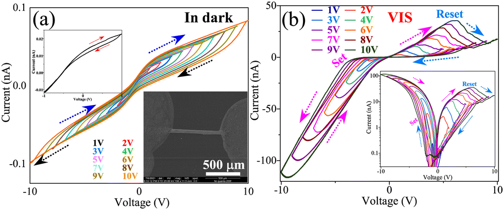 | ||
| Fig. 2 At different bias voltages, cyclic I–V characteristics. (a) In the dark. The lower right inset is a FESEM image of a single micro/nanowire based two-terminal device, and the upper left inset represents the I–V curve at 1 V bias. (b) Under illuminating the whole devices with 7.72 mW cm−2 VIS. The inset is their corresponding semi-logarithm pattern. | ||
Under illuminating with VIS, all the I–V curves show two asymmetric hysteresis loops at the range of bias from 1 to 10 V, presenting typical characteristics of bipolar RS, as described in Fig. 2b. In the forward-biased direction, the hysteresis loops circulate clockwise, and contrarily they circulate counterclockwise in the backward-biased direction. Moreover, with the increase of the testing bias from 1 to 10 V, the hysteresis loops gradually stabilize from “slingshot like” at 1 V to asymmetric oblique cross “8”, suggesting that the bias voltage has a great impact on the hysteresis behaviour of electrical transport of the device. At a relatively low bias, the photocurrent is greater in the forward-biased direction than that in backward-biased direction, while when the applied bias voltage exceeds 3 V, it is just the opposite that the photocurrent increases gradually in the backward-biased direction with the increase of bias. At a large operation bias, the photocurrent in the forward-biased direction firstly increases gradually at the relatively low voltage; however, as the voltage increases, the photocurrent increases slowly, or even decreases at a higher voltage. The results demonstrate that a more obvious asymmetric effect with a bipolar RS feature can be induced by a larger bias, and the photoresponse can also be strongly regulated by the external bias.
To further explore the influence of illumination intensity on the performance of electrical transport, the I–V characteristics were measured by illuminating the entire device with different intensities of VIS at 4 V bias, as shown in Fig. 3. As seen from Fig. 3a, the I–V curves show asymmetric hysteresis loops with a bipolar RS feature with the increase of the incident light power. Moreover, in the forward-biased direction, the NDR peak gradually shifts in the large voltage direction, and meanwhile the hysteresis behaviour becomes more and more remarkable. When the incident light power is 1.4, 3.4, 6.9, 12.2 and 23.3 mW cm−2, respectively, the corresponding conversion voltages (reset voltage) are 1.6, 2.2, 2.3, 2.5 and 2.7 V. Therefore, with the same operation bias, the reset voltage from LRS to HRS can be effectively controlled by the incident light intensity.
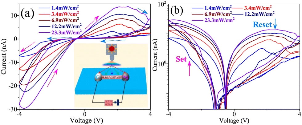 | ||
| Fig. 3 (a) Under illuminating the entire device with different intensities of VIS, cyclic I–V characteristics at 4 V bias. The inset corresponds to a diagrammatic sketch of the device under illuminating the entire device. (b) Corresponding semi-logarithm pattern. | ||
3.3 Application in nonvolatile optical memory for the asymmetric devices with adjustable hysteresis
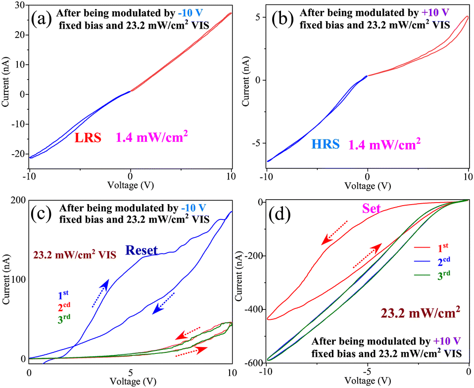
In the asymmetric device, the bias and illumination dependence of the bipolar RS characteristics indicate a huge potential in optical RRAM storage applications. To investigate in detail its performance, memory properties were tested at different biases under illuminating with VIS, as described in Fig. 4. From the multiple write–read–erase–read processes shown in Fig. 4a, it can be seen that the device can exhibit an excellent cycling stability and repeatability, where −6, +6, and +0.02 V are used as the writing, erasing, and reading voltages, respectively. Fig. 4c corresponds to the enlarged view of one write–read–erase–read process in the purple part of Fig. 4a. It can be seen that the device can be set to LRS after being applied with a −6 V fixed bias and reset to HRS after being applied with a +6 V fixed bias. In the whole testing process, the device shows a switching ratio (ILRS/IHRS or RHRS/RLRS) of more than 40 times, suggestive of an excellent storage performance and cycling stability.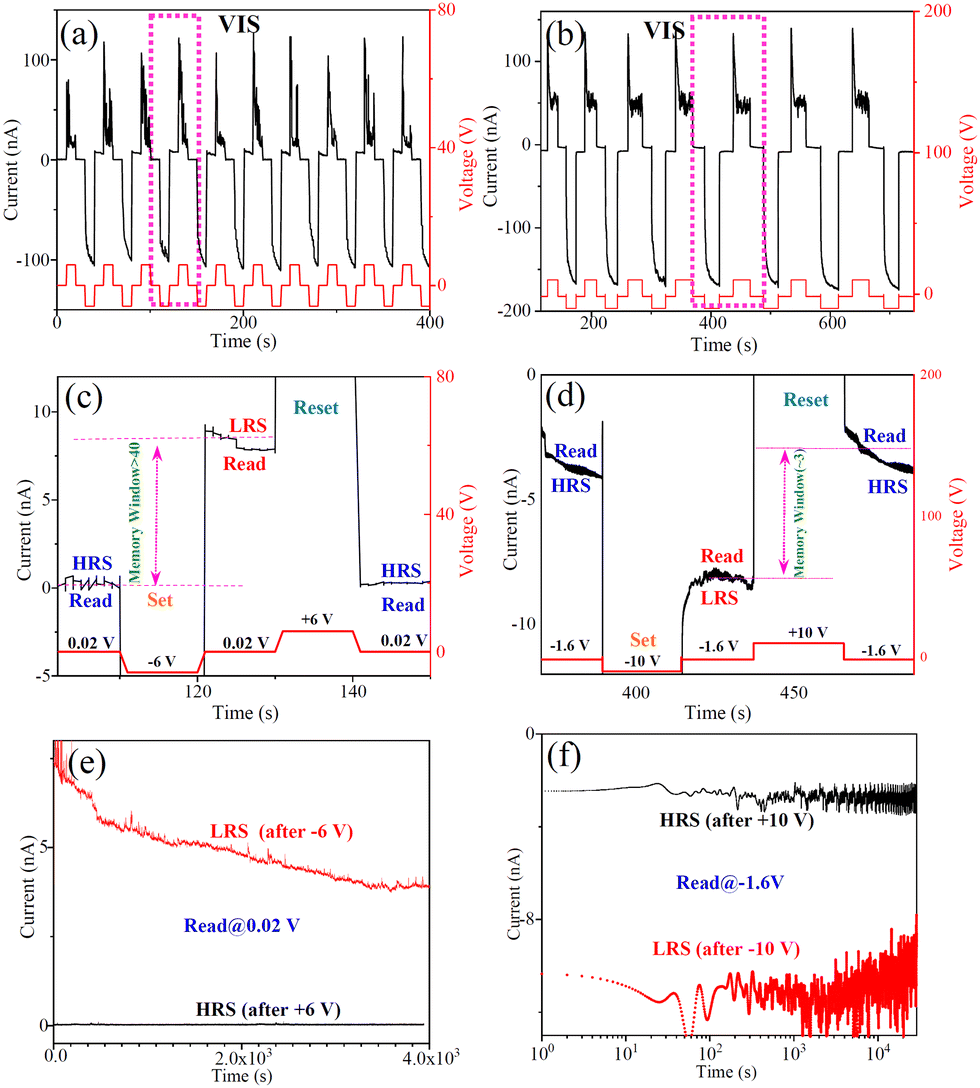 | ||
| Fig. 4 Nonvolatile memory performance of the asymmetric two-terminal device based on a single CH3NH3PbI3 micro/nanowire under illuminating with VIS. (a) Multiple cyclic processes of writing–reading–erasing–reading. The reading, writing, and erasing voltages are set as 0.02, −6 and +6 V, respectively. (b) Multiple cyclic processes of writing–reading–erasing–reading. The reading, writing, and erasing voltages are set as −1.6, −10 and +10 V, respectively. (c and d) Enlarged views of the dotted pink frames in (a and b), respectively, showing a detailed writing–reading–erasing–reading process with a memory window of about 40 and 3 times. (e and f) Retention of the stored data for the modulated HRS and LRS at 0.02 and −1.6 V reading voltages, respectively. | ||
To further explore the storage performance at a negative reading voltage, −1.6 V was selected as a reading voltage, and similarly −10 and +10 V were used as writing and erasing voltages, respectively, as illustrated in Fig. 4b. After being applied with a −10 V fixed bias, the device can show a small negative current, and meanwhile display an HRS at −1.6 V reading voltage. After being applied with a +10 V fixed bias, conversely, the device can show a large negative current and meanwhile present an LRS at the same reading voltage. In addition, the device can also show a good nonvolatile memory feature after multiple cycles. To clearly investigate the storage characteristics, simultaneously, Fig. 4d shows an enlarged view of a single write–read–write–read cycle process in the purple part of Fig. 4b, from which a storage window of about 3 times can be observed.
To ascertain the stability of the storage performance, the HRS and LRS retention characteristics were tested at a read voltage of +0.02 and −1.6 V, respectively, as shown in Fig. 4e and f. As can be seen from Fig. 4, the ratio of resistance switching under a positive reading voltage of +0.02 V is almost 10 times larger than that under a negative reading voltage of −1.6 V. However, the HRS current at −1.6 V reading voltage only shows a slight variation after about 103 s, and almost maintains an initial regulation value, demonstrating an excellent nonvolatile memory effect, while on the other hand, the HRS current decreases slowly at +0.02 V reading voltage and then remains in a relatively small current state. Interestingly, the current state of the CH3NH3PbI3 micro/nanowire-based asymmetric two-terminal device is not a simple abrupt RS at the Ag electrode under a weak illumination, but a slowly changing behavior of memristor, similar to the brain-like learning processes in biology. Moreover, at the reading voltages of 0.02 and −1.6 V, respectively, the devices all show remarkable nonvolatile characteristics, and meanwhile present different levels of resistance states. For this multilevel nonvolatile memory characteristic, it can be expected to apply in the field of optical nonvolatile RRAM.
3.4 Application in logic or gate operation for the asymmetric devices with tunable hysteresis with bias and illumination
Based on the above testing results, the I–V curves can show a certain asymmetric hysteresis effect in the dark and under VIS. The electrical performance of the Ag/CH3NH3PbI3/C two-terminal device in logic OR gate operation was deeply studied, as shown in Fig. 5a and b. The “OR gate (C = A + B)” logic circuit was designed, where the input source A represents applied bias, the input source B signifies VIS illumination, and the output C corresponds to current, as shown in Fig. 5e. The basic logic operation can be realized by dark-write/bias-erase and light-write/bias-erase operation in the Ag/CH3NH3PbI3/C two-terminal device.2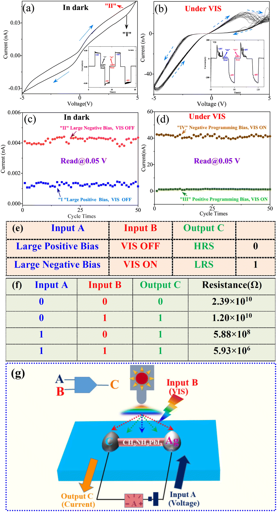 | ||
| Fig. 5 Logic OR gate operation characteristics of an asymmetric two-terminal device based on a single CH3NH3PbI3 micro/nanowire. (a) At 5 V bias, the I–V curve in the dark. The inset corresponds to the I–T curve at 0.05 V reading voltage, executing “00” and “01” which correspond to “I” and “II” resistance states of the logic OR gate, respectively. (b) At 5 V bias, multicyclic I–V curves under illumining with VIS. The inset corresponds to the I–T curve at 0.05 V reading voltage, executing “10” and “11” which correspond to “III” and “IV” resistance states of the logic OR gate, respectively. (c) After executing “00” and “01”, respectively, the cyclic stability curves of “I” and “II” resistive states. (d) After executing “10” and “11”, respectively, the cyclic stability curves of “III” and “IV” resistive states. (e and f) Truth table and corresponding output resistance values of OR gate logic operation. Input source A is external loading bias, and signals “1” and “0” represent negative and positive biases, respectively. Input light source B is the illumination intensity of the light source, where “0” and “1” represent light off and on, respectively. (g) Schematic diagram of the inductive logic OR gate under VIS and bias. | ||
For the input A, the +10 and −10 V voltages are defined as signal 0 and 1, respectively. While for the input B, VIS OFF and ON are defined as signal 0 and 1, respectively, and for the output C, the low current and large current at the reading voltage of 0.05 V, which correspond to HRS and LRS, are defined as signal 0 and 1, respectively. For the whole asymmetric device, if one or two inputs are signal 1, the output is always signal 1 (large current and LRS), and only when both inputs are signal 0, the output is signal 0 (low current and HRS). Therefore, when different operation commands are executed, the device can be switched between four resistance states (I, II, III and IV), showing the ability to implement logic OR gates, and moreover the nonvolatile states, as shown in Fig. 5c and d. For output signal C, HRS (resistance > 2 × 10¹⁰ Ω) is defined as 0, and LRS (resistance < 2 × 10¹⁰ Ω) is defined as 1. Fig. 5e and f show the truth table and corresponding output resistance values of an OR gate logic operation. Regardless of the initial resistance state of the device, it can output the results of OR gate logic operation. When the logic operations illustrated in Fig. 5a and b are performed (i.e., the input logic values are 00, 01, 10 and 11), respectively, the results with different resistance states (I, II, III and IV) are expected to be the logic OR gate operation results. After multiple cycle tests, the repeatability of the nonvolatile logic operation of the device can be well maintained, as shown in Fig. 5c and d.
The above results show that logic OR gate operations similar to a computer can be efficiently realized by the optical adjustable hysteresis effect of the I–V characteristics of the asymmetric single CH3NH3PbI3 micro/nanowire based two-terminal device, and show recyclable repetitive resistance states, indicating huge prospects for application. Therefore, for the asymmetric two-terminal device based on a single CH3NH3PbI3 micro/nanowire, its two electrodes can show different photoresponse performance due to a difference of interfacial state induced by chemical composition. They can not only show unique multilevel nonvolatile storage characteristics when applying different writing and reading voltages, but also execute simple logic OR gate operation with electrical and optical signals as input sources. The device, integrated with multifunctional optical properties, can directly process and store photoelectric signals. It is expected to realize the synchronization of computing and storing function, resulting in a good application potential in breaking through the traditional von Neumann bottleneck.
3.5 Physical origin of tunable hysteresis with bias and illumination in a single perovskite micro/nanowire-based asymmetric device for optical nonvolatile memory and logic OR gate operation
Compared with the activation energy of Pb2+ (0.8–0.23 eV) and MA+ (0.46–0.84 eV), that of I− is only 0.1–0.6 eV, which is much smaller.53 Therefore, under the action of an external electric field, it is possible for I− to diffuse into the Ag electrode, and similarly it is also possible for Ag to enter the CH3NH3PbI3 lattice, while when the C electrode is loaded with a relatively large positive and negative voltage, it is very difficult for the accumulation of I− and Ag+ at the end of C electrode to be observed and verified. For the bipolar RS based on CH3NH3PbI3, the formation and rupture of the conductive filament from active metal ions,54–56 iodide ions,57 and iodine vacancies58–61 is the most popular mechanism proposed at present to explain the switching effect. For the device based on a 1D CH3NH3PbI3 micro/nanowire with a large length–diameter ratio, it is extremely difficult to form conductive filaments between two electrodes, and moreover the I–V curves present a polar feature. For CH3NH3PbI3 micro/nanowires, however, they have a very large surface to volume ratio and typical p-type properties. Due to the destruction of the periodic asymmetry of the lattice on their surface, in addition, the presence of a large number of dangling bonds can induce the appearance of surface states. Since the energy gap of CH3NH3PbI3 is only 1.55 eV, it is easy to produce free electron–hole pairs under illumination of VIS.62 When the two ends of the device are constructed with Ag and C electrodes, respectively, different interface barriers associated with surface states can be formed, and an asymmetric back-to-back surface barrier-related diode connected with resistance in series is built. Thus, the bias and illumination-induced variation of electrode interfaces will be predominant for the electrical transport of the two-terminal device with asymmetrical Ag and C electrodes.To determine the origin of the nonvolatile storage effect and logic OR gate operation of the asymmetric two-terminal device based on a single CH3NH3PbI3 micro/nanowire, the curves of photogenerated voltage and current were first tested at 0 V bias under periodically illuminating different regions of the device with VIS to verify the presence of an interface barrier, as shown in Fig. 6. It can be seen that the photogenerated voltage and current are the largest under illuminating the entire device, which can reach 0.016 V and 0.18 nA, respectively, indicating that the device not only exhibits an interface barrier, but also can be used as a self-powered voltage source without external bias. When illuminating the vicinity of the C electrode, the photogenerated voltage and current are the smallest. At the end of the Ag electrode, moreover, all the potentials are negative whether illuminating the entire device, Ag electrode or C electrode. Due to the formation of the back-to-back surface barrier-related diodes and the p-type properties of the CH3NH3PbI3 semiconductor, the surface barrier is much larger at the Ag electrode interface than at the C electrode interface, where the interface barrier plays a decisive role in photogenerated voltage and current at 0 V bias under illumination. Therefore, it can be concluded that the two-terminal device presents a distinct interface photovoltaic (PV) effect, and moreover it mainly comes from the interface of the Ag electrode.
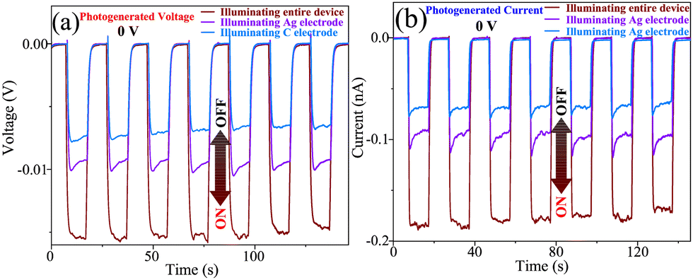 | ||
| Fig. 6 At 0 V bias, photogenerated voltage and current under periodically illuminating different regions of the device. (a) Photogenerated voltage. (b) Photogenerated current. | ||
To further prove the bias-induced height variation of the interface barriers at two different electrodes, after being regulated by +10 and −10 V fixed biases under illuminating the entire device, Ag electrode, and C electrode with 23.2 mW cm−2 strong VIS, the I–V characteristics of the asymmetrical two-terminal device were measured at a low bias no matter how the illumination regions with 1.4 mW cm−2 weak VIS varied. All I–V curves deviated upwards from the zero point. This further confirms that the surficial PV effect mainly comes from the interface of the Ag electrode and furthermore the potential of the Ag electrode is negative. As seen from Fig. 7a and b, after being applied with −10 V fixed bias, all open circuit voltages (Voc) increase compared with the modulation of +10 V fixed bias under illuminating the entire device, Ag electrode and C electrode, suggesting that the interface barrier height of the Ag electrode increases. Moreover, their short-circuit currents (Isc) increase as well, indicating that the decrease of the interface barrier width of the Ag electrode reduces the resistance of the entire device. Under only illuminating one electrode, I–V characteristics were measured as well. From Fig. 7c–f, it can be seen that the change of the interface barrier height is more apparent under illuminating the Ag electrode than the C electrode. This further reveals that bias can trigger a larger variation of the interface barrier of the Ag electrode than that of the C electrode.
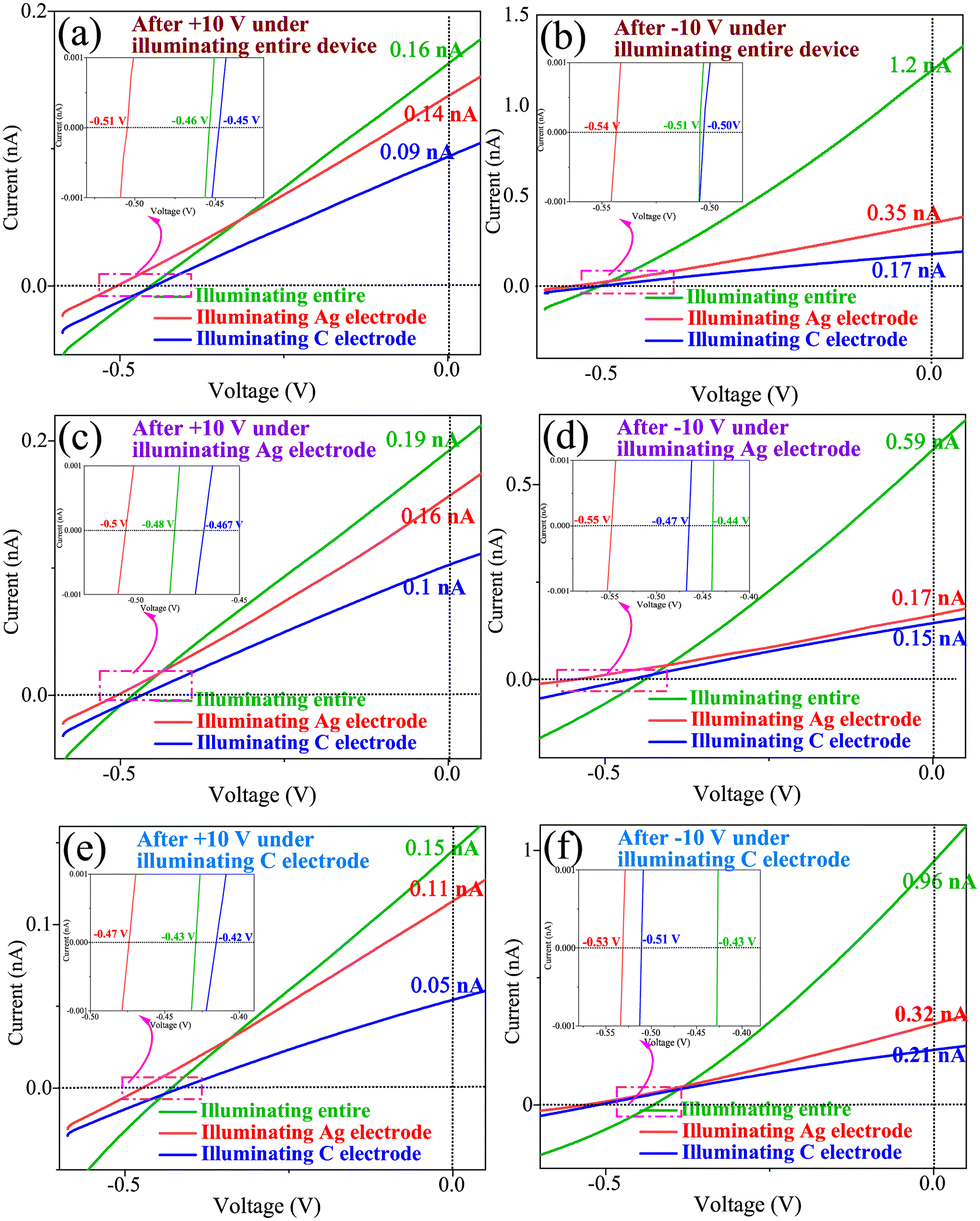 | ||
| Fig. 7 After being modulated by +10 and −10 V fixed bias under illuminating different regions with a strong incident VIS of 23.3 mW cm−2, respectively, the I–V characteristics of the asymmetric two-terminal device under illuminating different regions with a weak VIS of 1.4 mW cm−2 at 0.6 V bias. (a and b) Modulated under illuminating the entire device with +10 and −10 V fixed bias, and the insets correspond to an enlarged view for the purple red parts. (c and d) Modulated under illuminating the vicinity of the Ag electrode with +10 and −10 V fixed bias, respectively, and the insets correspond to an enlarged view for the purple red parts. (e and f) Modulated under illuminating the vicinity of the C electrode with +10 and −10 V fixed bias, respectively, and the insets correspond to an enlarged view for the purple red parts. | ||
To further explore the influence of the interface barrier on the photoresponse of asymmetric devices, a microbeam light from an optical microscope was used to irradiate the vicinity of two end electrodes at different bias amplitudes and illumination intensities, as shown in Fig. 8. It can be clearly seen that the I–V curves all show a certain hysteresis behaviour under illuminating near the Ag and C electrodes, respectively. Although they are somewhat like the asymmetric “8” shape under illuminating the entire device, there still exist obvious differences. As seen from Fig. 8a, when the vicinity of the forward-biased Ag electrode is illuminated, hysteresis loops with a clockwise cycle appear in the forward-biased direction, and moreover the NDR behaviour is more conspicuous as well. In addition, the hysteresis behaviour increases significantly with the increase of the applied bias from 2 to 10 V, demonstrating a noticeable effect of bias on the hysteresis behaviour and a more likely elicitation of the hysteresis effect by a larger applied bias. However, when the backward-biased C electrode is illuminated, there exist distinguishable hysteresis loops with a counterclockwise cycle in the backward-biased direction, and unfortunately there is almost no hysteresis effect in the forward-biased direction, which is exceedingly different from the curves when illuminating the forward-biased Ag electrode, further manifesting that the hysteresis behaviour should originate from the effect of the electrode interface. Similarly, the hysteresis effect gradually increases with the increase of the applied bias voltage, which further proves that the bias voltage has a certain regulation on the hysteresis effect of the device, as shown in Fig. 8b. More importantly, the hysteresis with NDR effect is more obvious in the forward-biased direction than in the backward-biased direction, suggestive of a great difference between the two electrode interfaces. The larger the bias is, the greater the hysteresis effect is, which can be attributed to the difference of the interface states at the interface of the two electrodes.
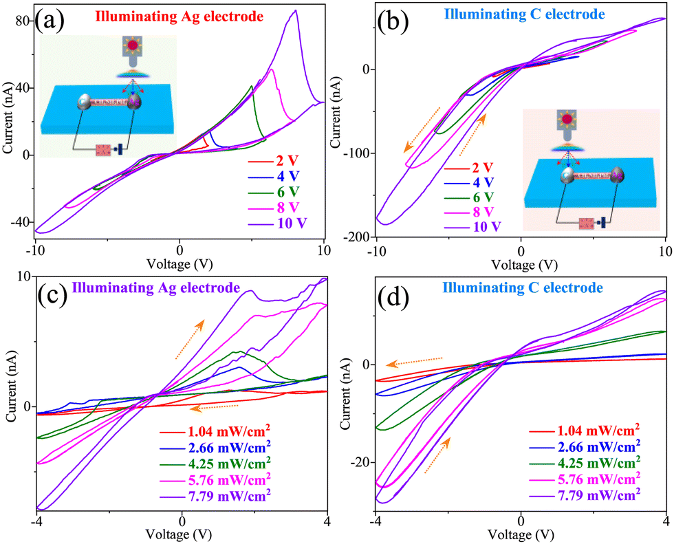 | ||
| Fig. 8 Under illuminating Ag and C electrodes with different illumination intensities and bias amplitudes, respectively, I–V characteristics of the two-terminal device. (a) At different biases, I–V curves under illuminating the vicinity of the forward-biased Ag electrode with 7.79 mW cm−2. The inset represents a diagrammatic sketch of the device under illuminating the Ag electrode. (b) At different biases, I–V curves under illuminating the vicinity of the backward-biased C electrode with 7.79 mW cm−2. The inset represents a diagrammatic sketch of the device under illuminating the C electrode. (c) Under illuminating the vicinity of the Ag electrode with different intensities of VIS, the I–V curves at 4 V bias. (d) Under illuminating the vicinity of the C electrode with different intensities of VIS, the I–V curves at 4 V bias. | ||
On the other hand, when different illumination intensities of 1.04, 2.66, 4.25, 5.76 and 7.79 mW cm−2 are applied, respectively, it can be found that all I–V curves present asymmetric hysteresis loops with bipolar RS features whether the vicinity of the Ag or C electrode is illuminated. Moreover, the currents both increase with the increase of the incident light power in the forward- and backward-biased directions, and the hysteresis effect is also becoming more and more prominent, as shown in Fig. 8c and d. Interestingly, when the vicinity of the Ag electrode is illuminated, both the photocurrent and NDR effect increase surprisingly with the increase of the incident light power density; however, the conversion voltage is almost unchanged, proving that there also exists a significant influence of light intensity on the electrode interface. However, when the vicinity of the C electrode is illuminated, the hysteresis effect becomes more noteworthy with the increase of the incident light power in the backward-biased direction. Although the current also increases in the forward-biased direction, the NDR effect does not appear. Moreover, compared with the illumination of the Ag electrode, the overall current is relatively low, indicating that the effect of light on the C electrode interface is relatively weak, as shown in Fig. 8d. This phenomenon not only proves the decisive role of light intensity on the interface states of the two electrodes, but also shows a great difference between the two-electrode interfaces. In addition, the electrode interface can be adjusted by the intensity of the incident light. When the Ag and C electrodes are irradiated with VIS, respectively, the hysteresis effect will increase with the increase of the bias amplitude and illumination intensity. At the same time, the induced photocurrent is much larger under illuminating the vicinity of the Ag electrode than C electrode. This fully proves that there exists a difference between the two electrode interfaces, and the bias amplitude and illumination intensity have a synergistic effect on the variation of the interface states.
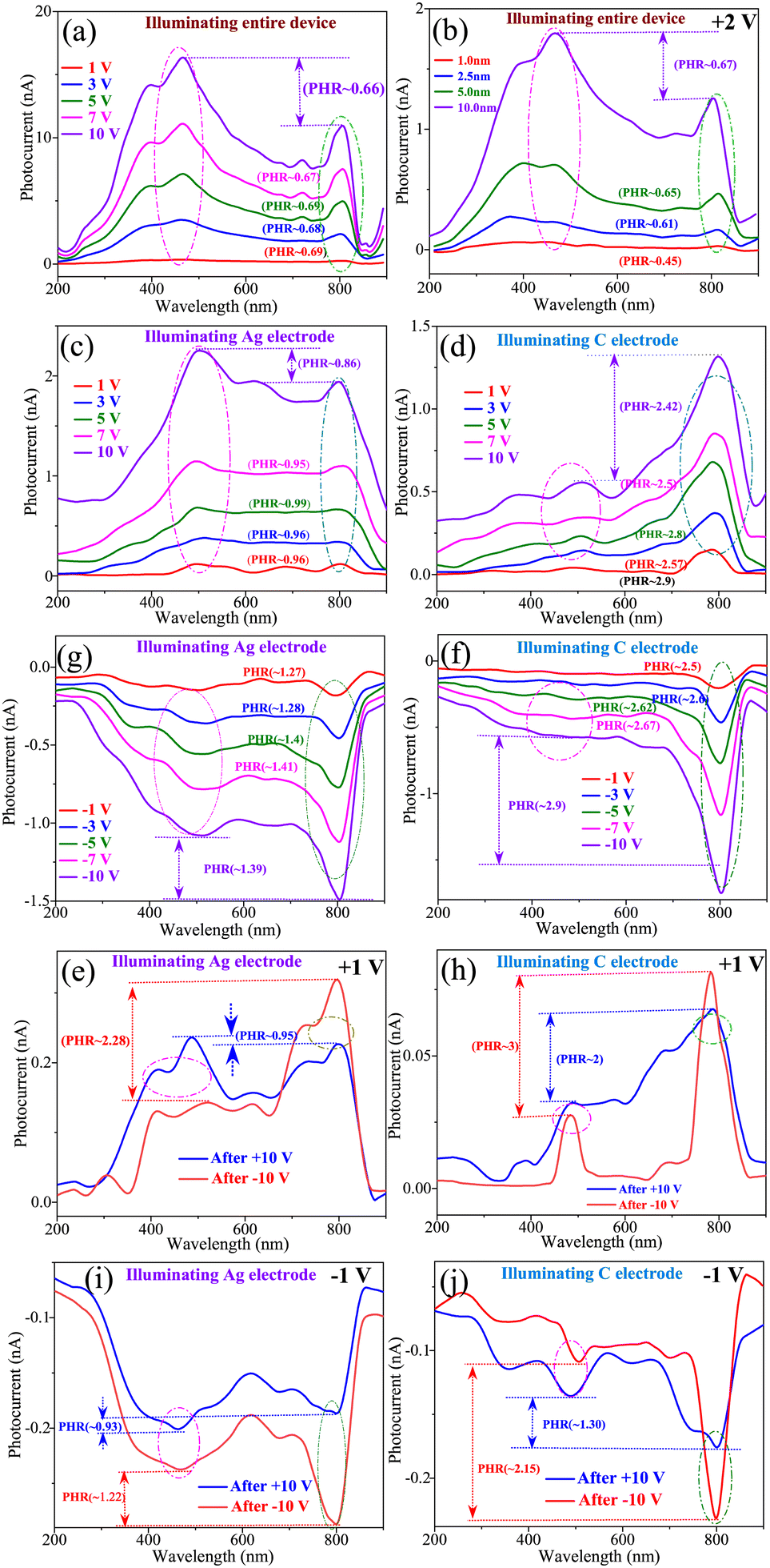
To further prove the influence of the electrode interface, the continuous photoresponse curves of the asymmetric devices were tested under different conditions in the wavelength range from 200 to 900 nm, as shown in Fig. 9. When illuminating the entire device, a strong photoresponse to the full spectrum in the range of 300–850 nm can be observed, where the two strong wide peaks appear at 380–550 and 750–850 nm, respectively, which can be attributed to the response peak of the product after the reaction between Ag and perovskite and the band gap peak of the CH3NH3PbI3 perovskite material itself. To better investigate the influence of external conditions on the continuous spectral photoresponse, the maximum current of the peak between 380–550 nm is defined as the impurity current (Iimp), while the maximum current of the peak from 750 to 850 nm is defined as the perovskite current (Iper), and the ratio of Iper to Iimp is defined as the peak height ratio (PHR). The greater the PHR is, the stronger the perovskite photoresponse is; conversely, the smaller the PHR is, the stronger the photoresponse of impurities is, so as to more accurately describe the variation of the spectral photoresponse peak. As seen from Fig. 9a, the PHR value gradually decreases from 0.69 to 0.66 with the increase of the applied fixed positive bias, indicating that the photoresponse peak at 380–550 nm becomes stronger and hence higher forward-biased voltage is more conducive to the photoresponse of impurities. As seen from Fig. 9b, on the contrary, the PHR shows an obvious increase from 0.45 to 0.67 with the increase of the incident light intensity, which also proves that the perovskite photoresponse peak is more obvious under higher illumination intensity. This phenomenon fully shows that a larger forward-biased voltage is more advantageous to the photoresponse to short wavelength light, while a stronger incident light intensity is more beneficial to the photoresponse to long wavelength light at the same forward-biased voltage.
 | ||
| Fig. 9 Spectral response curves of the device under continuous fluorescence irradiation in the range of 200–900 nm. (a) At different fixed biases, spectral response under illuminating the entire device. (b) At different illumination intensities, spectral response under illuminating entire device at a fixed bias of +2 V. (c and d) At different positive fixed biases, the spectral response under illuminating the end of the Ag and C electrodes with different intensities, respectively. (e and f) At different negative fixed biases, the spectral response under illuminating the Ag and C electrodes with different intensities, respectively. (g and h) After being modulated by +10 and −10 V fixed biases, the spectral response under illuminating the Ag and C electrode at +1 V fixed bias. (i and j) After being modulated wih +10 and −10 V fixed biases, the spectral response under illuminating the Ag and C electrodes at −1 V fixed bias, respectively. | ||
To fully understand the interface variation of asymmetric devices under applying illumination and bias, the spectral response was tested in the range of 200–900 nm under irradiating the vicinity of the Ag and C electrodes at different fixed forward-biased biases, respectively, as illustrated in Fig. 9c and d. When the vicinity of the Ag electrode is illuminated, all the PHR is less than 1 at the fixed bias ranging from +1 to +10 V, indicating that the peak of the impurity photoresponse is stronger than that of the band gap photoresponse of perovskite materials at the interface of the Ag electrode, and moreover the PHR gradually decreases with the increase of the fixed bias. When the fixed bias increases from +1 to +10 V, the PHR also gradually decreases from 0.9 to 0.84, indicating that the impurity photoresponse is getting stronger and stronger. According to the wavelength range of the impurity peak from 380 to 550 nm and the possible reaction, it can be speculated that the chemical reaction has taken place at the Ag electrode interface. The Ag electrode may react with CH3NH3PbI3 perovskite materials to form some AgIx and PbI2 compounds, which correspond to the photoresponse peaks near 400 to 500 nm, respectively.63–66 In the spectral response curve, the stronger the applied bias is, the stronger the peak of the impurity photoresponse is, which further proves the regulation effect of positive bias on the reaction at the interface of the Ag electrode. On the contrary, when the vicinity of the C electrode is illuminated, all the PHR is greater than 1 at the bias from +1 to +10 V, indicating that the photoresponse of perovskite is stronger than that of impurities, and this difference is very measurable. Moreover, with the increase of the bias voltage, the PHR value also gradually increases, indicating that the photoresponse of the perovskite at 750–850 nm becomes stronger. Although the peak of the impurity photoresponse also increases, it is still much smaller than that of the perovskite photoresponse. This phenomenon demonstrates that there is no chemical reaction at the interface of the C electrode. Although the photoresponse of impurities is also slightly enhanced, it can be ignored compared with that of the perovskite. Therefore, it shows a simple and obvious perovskite photoresponse peak, which further proves the role of the Ag electrode in this process. Interestingly, by comparing the continuous spectral photoresponse peaks under illuminating Ag and C electrodes, respectively, it can be found that the photocurrent under illuminating the Ag electrode is greater than that under illuminating the C electrode at the same bias voltage, indicating that the photoresponse is stronger at the interface of the Ag electrode than that at the interface of the C electrode. This also implies that there exist different mechanisms at the interfaces of the Ag and C electrodes. The change of the interface barrier at the interface of the Ag electrode and perovskite material is caused by an irreversible reaction, while at the interface of the C electrode, the barrier change is caused by the capture and emission of holes in interfacial traps, which proves that the bias has different modulation effects on different interfaces.
To further prove this hypothesis and the impact of bias polarity, accordingly, the spectral responses were tested as well at different fixed backward-biased voltages under illuminating the Ag and C electrodes, respectively, as illustrated in Fig. 9e and f. At negative fixed biases, the photoresponse is similar to that at positive fixed biases with some differences. When the vicinity of the Ag electrode is illuminated, the PHR basically increases from 1.27 to 1.39 with the increase of the negative fixed bias from −1 to −10 V, which proves that the negative fixed bias is more conducive to the photoresponse near 800 nm and further indicates an occurrence of reduction reaction at the Ag electrode where some perovskite phases are regenerated. However, the response peak at 500 nm is still strong due to the existence of some AgIx at the Ag electrode interface. On the contrary, when the C electrode is illuminated, the spectral response is basically the peak at about 800 nm at negative fixed biases, and even a small part of the response peak at 500 nm is almost invisible, which proves the occurrence of AgIx reduction reaction at the Ag electrode interface.
To further prove the effect of external bias and nonvolatile memory effect, the continuous spectral response was further tested at +1 V fixed small bias after being applied with +10 and −10 V large fixed bias, respectively, as shown in Fig. 9g and h. After being applied with a relatively large +10 V fixed bias, the photoresponse peak of the impurity peak between 380–550 nm becomes stronger when the vicinity of the Ag electrode is illuminated, and the PHR is about 0.94. While after being applied with −10 V fixed bias, the photoresponse peak between 750–850 nm is stronger, and the PHR is about 2.4, showing a completely opposite phenomenon, which shows that the oxidation and reduction reactions of Ag can occur after being regulated by +10 and −10 V fixed bias, respectively. However, when the negative C electrode is illuminated, the photoresponse peaks of the perovskite between 750–850 nm are both strong, and the PHR is around 3 and 2 after being regulated by −10 and +10 V fixed bias, respectively, which also indicates that the photoresponse of perovskite is stronger after the C electrode is applied with a negative voltage, and in contrast the photoresponse of impurities is stronger after being applied with a positive voltage. The photoresponse of impurities is stronger at the Ag electrode than at the C electrode, and therefore this can also prove firmly that the impurity should be mainly AgIx rather than PbI2.
After being modulated by +10 and −10 V fixed biases, the spectral response was also measured at −1 V fixed bias under illuminating the Ag and C electrodes, respectively, as presented in Fig. 9i and j. The impurity photoresponse peak is more obvious after being applied with +10 V than after being applied with −10 V fixed bias under illuminating the Ag electrode. Conversely, the perovskite photoresponse peak is more obvious after being applied with −10 V than that after being applied with +10 V fixed bias under illuminating the C electrode. The phenomenon is slightly different from that at +1 V, but is consistent as a whole, which further proves the previous speculation. Moreover, the feature modulated by a relatively large fixed bias of 10 V presents a nonvolatile memory effect. After being regulated by +10 and −10 V, oxidation and reduction reactions occur at the Ag electrode interface, resulting in different spectral responses, and the appearance of the NDR effect in the direction of forward-biased voltage.
To further understand the origin of the hysteresis behavior and corresponding RS performance, after being modulated by +10 and −10 V fixed bias under illuminating the entire device with 23.2 mW cm−2 strong VIS, I–V characteristics were measured under illuminating with different intensities of VIS at a unipolar cyclic bias, as shown in Fig. 10. As seen from Fig. 10a, the I–V characteristics, modulated by −10 V fixed bias and re-measured under illuminating with weak light at a unipolar cyclic bias between 0 and 10 V, is almost linear in the forward-biased direction, with a distinguishable saturation region at relatively large voltage. As seen from Fig. 10b, the current is relatively low after being modulated by +10 V fixed bias compared with −10 V modulation. In the forward-biased direction, the current is relatively low at low bias; however, it quickly increases at large bias. Conversely, it shows more obvious saturation in the backward-biased direction. This demonstrates that the width of the interface barrier of the C electrode is relatively narrow, and moreover it becomes relatively wide after being applied with a large forward-biased voltage and contrastingly becomes narrow after being applied with a large forward-biased voltage. Therefore, its electrical transport is mainly controlled by thermionic emission. For the interface barrier of the Ag electrode, it becomes very narrow after being modulated by −10 V fixed bias, and its electrical transport is completely controlled by the barrier height dependence of thermionic emission. After being modulated by +10 V fixed bias, however, the surface space charge region becomes very wide, which is much larger than the average free path of electrons, and hence its electrical transport is mainly controlled by the voltage dependence of hole diffusion. This clearly confirmed that the resistance variation mainly originates from the width variation of the interface barrier of the Ag electrode.
 | ||
| Fig. 10 After being modulated by +10 and −10 V fixed bias under illuminating the entire device with 23.2 mW cm−2 strong VIS, I–V characteristics measured under illuminating with different intensities of VIS at a unipolar cyclic bias. (a) After being modulated by −10 V fixed bias, measured under illuminating with weak light at a unipolar cyclic bias between 0 and ±10 V. (b) After being modulated by +10 V fixed bias, measured under illuminating with weak VIS light at a unipolar cyclic bias between 0 and ±10 V. (c) After being modulated by −10 V fixed bias, measured under illuminating with strong light at a forward-biased unipolar cyclic bias between 0 and +10 V. (d) After being modulated by +10 V fixed bias, measured under illuminating with strong light at backward-biased unipolar cyclic bias between 0 and −10 V. | ||
From Fig. 10c, it can be seen that the I–V curve shows a clockwise hysteresis loop with NDR effect at the first cycle under illuminating with strong VIS after being modulated by −10 V fixed bias and strong VIS, and then transforms into an HRS. In the subsequent operation with unipolar forward-biased cyclic I–V curves, the NDR effect disappears, and moreover their shapes are almost close with very weak hysteresis effect with counterclockwise cycle. As seen from Fig. 10d, the I–V curve shows a counterclockwise hysteresis loop at the first cycle under illuminating with strong VIS after being modulated by +10 V fixed bias and strong VIS, and then transforms into an LRS. In the subsequent operation unipolar backward-biased cyclic I–V curves, their shapes are almost close and the hysteresis loops almost disappear as well. The hysteresis loops only appear at the first cycle under successively unipolar cyclic scanning bias after being applied with opposite large bias, indicating that the asymmetric hysteresis with bipolar RS feature occurs only after being applied with an opposite voltage. It also shows that the HRS and LRS are strongly related to the voltage polarity, and moreover it is more reasonable to originate from the variation of the electrode interface rather than ion transfer.
It can be concluded that the variation of the Ag electrode interface should come from a voltage-induced in situ reversible reaction under illuminating rather than ion transfer. When the Ag electrode is illuminated, some chemical bonds are broken, and therefore some free I− ions can be formed, and meanwhile Ag can be oxidized to Ag+ at a relatively large voltage and then react with I− ions to form AgIx, resulting in an enhancement of the interface combination. Consequently, the Ag electrode interface can show a superior photoresponse and PV effect. However, the resistivity of AgIx is relatively large. At larger positive voltage, the surface depletion region becomes much broader, and moreover its width is larger than the average free path of electrons, and hence its interfacial electrical transport is mainly dominated by the voltage dependence of hole diffusion. Accordingly, the device transforms into an HRS after the formation of AgIx. Conversely, at a relatively large negative voltage, the reduction reaction can lead to a disappearance of AgIx. Although the height of the interface barrier increases, its width decreases remarkably, and thereby its interfacial electrical transport is completely controlled by the barrier height dependence of thermionic emission, which is more conducive to the photoresponse, resulting in an LRS.
At the interface of the C electrode, the redox reaction hardly occurs between C and the ions in CH3NH3PbI3 even at a large bias and strong illumination. However, the surface states of the CH3NH3PbI3 micro/nanostructure can be well kept, and moreover there exist quantities of trap centers in its surface space charge region. At a large backward-biased voltage, hence, holes can be injected into the traps from the C electrode, resulting in a filling of traps. The surface Fermi level shifts downwards, resulting in a decrease of the height and width of the surface barrier, and hence its interfacial electrical transport is mainly controlled by thermionic emission. At a large forward-biased voltage, on the contrary, the height and width of the surface barrier increases due to the ejection of holes from traps, and accordingly its interfacial electrical transport can transform from thermionic emission to hole diffusion. As a consequence, at a large forward-biased voltage, the AgIx layer with a high resistance state is formed at the interface of the Ag electrode, and meanwhile holes are ejected from the traps in the interface of the C electrode. Both barrier widths at the Ag and C electrode interfaces increase. Whether at a small forward- or backward-biased voltage, the device is nonconductive HRS after being applied with a relatively large fixed forward-biased voltage. After being applied with a relatively large fixed backward-biased voltage, the width of the surface barrier is very low at both the Ag and C electrodes. Therefore, the strong photoresponse effect leads to an appearance of LRS. The corresponding HRS and LRS schematic diagrams of bias and illumination regulation are illustrated in Fig. 11.
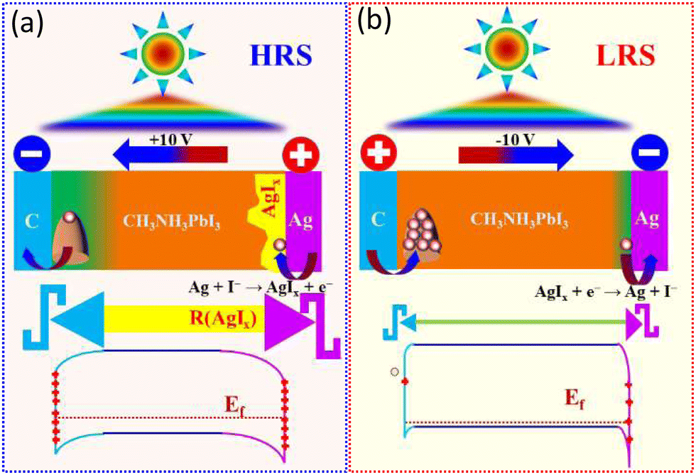 | ||
| Fig. 11 Schematic diagram of bias and illumination regulation of surface states in a single CH3NH3PbI3 micro/nanowire-based device with an architecture of Ag and C two-terminal electrodes under illuminating the entire device with VIS. (a) After +10 V fixed bias. (b) After −10 V fixed bias. | ||
Under regulating with a large voltage, the resistive memory effect of the device can be attributed to the bias and illumination-induced difference of the interfacial effect at the Ag and C electrode interfaces, which originates from the synergistic effect of the redox reaction at the Ag electrode interface and the injection and ejection of holes in the interfacial traps of the C electrode. Interestingly, this nonvolatile storage performance is different from a simple RS. Under a relatively weak illumination, a slow variation is similar to the process of the human brain, like synaptic learning. At the same time, when the Ag electrode reacts with the semiconductor, the multilevel resistance states introduced into the interface can show a hysteresis effect in the dark and under illumination. When a simple logic operation program is set, the device can perform logic OR gate operation. In the condition of different input resources, A and B, the output value C can show different resistance states, and the four different operation processes of “00”, “01”, “10”, and “11” can record and save the operation results by different resistance values. In a word, the asymmetric two-terminal device based on a single CH3NH3PbI3 perovskite micro/nanowire not only has excellent optical nonvolatile storage characteristics, but also can perform simple logic OR gate operation. This integrated optical operation and memory can simulate the operation, learning and storage process with only one device. Then, when multiple devices are connected in series or in parallel, it is expected to realize more complex operation. This idea is likely to provide a practical carrier for the concept of computer Deep Learning in the future.
4. Conclusions
In summary, by designing a two-terminal device based on a single CH3NH3PbI3 1D micro/nanowire with asymmetric Ag and C electrodes, the properties of electrical transport can be precisely controlled by the modulation of external bias and VIS. The device not only shows excellent photoresponse to VIS, but also presents a huge difference of photoresponse at the interfaces of the Ag and C electrodes, resulting in an appearance of illumination intensity and bias amplitude dependence of hysteresis behaviour. Importantly, the bias and illumination-modulated different HRS and LRS can be both maintained well at subsequent operation with low bias and weak illumination, showing an excellent optical nonvolatile memory effect with multiple levels. In the dark and under illumination, in addition, the difference of hysteresis effect makes it possible to perform logic operations when setting a specific logic OR gate input program, and output the operation results as current micro-signals. In the asymmetric two-terminal device based on a single CH3NH3PbI3 micro/nanowire, the existence of abundant surface states and different electrode interface responses leads to the formation of asymmetric interface effects. By microregion photoresponse testing of the I–V curves at a low operation bias after being regulated by different large biases under illuminating different regions with VIS, the underlying mechanism of controlled hysteresis can be attributed to the bias- and illumination-induced synergistic effect of interface barrier height and width variation related to the redox reaction of Ag ↔ Ag+ at the interface of the Ag electrode and the injection and ejection of holes in the interfacial traps of the C electrode. On the basis of the clear identification of the hysteresis mechanism, the electrical transport with hysteresis can be precisely controlled by suitable device design and external modulation. Not only can nonvolatile optical memory be realized, but by setting a specific logic gate program and bias regulation, the device can simulate computer operation, learning and storage processes. Therefore, it can be expected that organic–inorganic hybrid perovskite materials have great application potential in optical nonvolatile memory and logic OR gates and meanwhile will become potential candidate materials for the next generation of multifunctional integrated devices.Conflicts of interest
There are no conflicts to declare.Acknowledgements
This work was financially supported by the National Natural Science Foundation of China (51571107) and the Natural Science Foundation of Jiangxi Province (20202ACB202002, 20202ACB214002).References
- E. J. Fuller, S. T. Keene, A. Melianas, Z. Wang, S. Agarwal, Y. Li, Y. Tuchman, C. D. James, M. J. Marinella, J. J. Yang, A. Salleo and A. A. Talin, Science, 2019, 364, 570–574 CrossRef CAS PubMed.
- Q. Xia and J. J. Yang, Nat. Mater., 2019, 18, 309–323 CrossRef CAS PubMed.
- Q. Shi, F. X. Jiang, Y. Yu, H. X. Lin, Y. F. Kou, T. Miao, H. Liu, W. T. Yang, W. B. Wang, P. Cai, X. H. Xu, H. W. Guo, L. F. Yin and J. Shen, Adv. Electron. Mater., 2019, 5, 19300020 Search PubMed.
- W. Y. Kim, H. D. Kim, T. T. Kim, H. S. Park, K. Lee, H. J. Choi, S. H. Lee, J. Son, N. Park and B. Min, Nat. Commun., 2016, 7, 10429 CrossRef CAS PubMed.
- A. Nirmala, I. Mukkatt, S. Shankar and A. Ajayaghosh, Angew. Chem., Int. Ed., 2021, 60, 455–465 CrossRef CAS PubMed.
- G. M. Marega, Y. F. Zhao, A. Avsar, Z. Y. Wang, M. Tripathi, A. Radenovic and A. Kis, Nature, 2020, 587, 72–77 CrossRef PubMed.
- S. Seo, B. S. Kang, J. J. Lee, H. J. Ryu, S. Kim, H. Kim, S. Oh, J. Shim, K. Heo, S. Oh and J. H. Park, Nat. Commun., 2020, 11, 3936 CrossRef CAS PubMed.
- V. Sharma, J. Mater. Chem. C, 2021, 9, 16828–16842 RSC.
- F. C. Zhou, Y. H. Liu, X. P. Shen, M. Y. Wang, F. Yuan and Y. Chai, Adv. Funct. Mater., 2018, 28, 1800080 CrossRef.
- J. Borghetti, G. S. Snider, P. J. Kuekes, J. J. Yang, D. R. Stewart and R. S. Williams, Nature, 2010, 464, 873–876 CrossRef CAS PubMed.
- M. A. Zidan, J. P. Strachan and W. D. Lu, Nat. Electron., 2018, 1, 22–29 CrossRef.
- S. Batool, M. Idrees, S.-R. Zhang, S.-T. Han and Y. Zhou, Nanoscale Horiz., 2022, 7, 480–507 RSC.
- J. M. Yang, Y. K. Jung, J.-H. Lee, Y. C. Kim, S.-Y. Kim, S. Seo, D. A. Park, J. H. Kim, S. Y. Jeong, I. T. Han, J. H. Park, A. Walsh and N. G. Park, Nanoscale Horiz., 2021, 6, 987–997 RSC.
- Q. Xia and J. J. Yang, Nat. Mater., 2019, 18, 518 CrossRef CAS PubMed.
- V. A. Demin, V. V. Erokhin, P. K. Kashkarov and M. V. Kovalchuk, J. Appl. Phys., 2014, 116, 064507 CrossRef.
- W. Liu, M. Li, R. S. Guzzon, E. J. Norberg, J. S. Parker, M. Lu, L. A. Coldren and J. Yao, Nat. Photonics, 2016, 10, 190–195 CrossRef CAS.
- X. Z. Tian, L. F. Wang, J. K. Wei, S. Z. Yang, W. L. Wang, Z. Xu and X. D. Bai, Nano Res., 2014, 7, 1065–1072 CrossRef CAS.
- X. L. Chen, P. Huang, X. Zhu, S. X. Zhuang, H. C. Zhu, J. J. Fu, A. S. Nissimagoudar, W. Li, X. W. Zhang, L. Zhou, Y. Wang, Z. Y. Lv, Y. Zhou and S. T. Han, Nanoscale Horiz., 2019, 4, 697–704 RSC.
- Q. Liu, W. Yue, Y. Li, W. Wang, L. Xu, Y. Wang, S. Gao, C. Zhang, H. Kan and C. Li, Adv. Electron. Mater., 2021, 7, 2100366 CrossRef CAS.
- B. Sun, G. D. Zhou, L. F. Sun, H. B. Zhao, Y. Z. Chen, F. Yang, Y. Zhao and Q. L. Song, Nanoscale Horiz., 2021, 6, 939–970 RSC.
- Y. Wang, Y. Zheng, J. Gao, T. Jin, E. Li, X. Lian, X. Pan, C. Han, H. Chen and W. Chen, InfoMat, 2021, 3, 917–928 CrossRef CAS.
- E. J. Yoo, M. Lyu, J. H. Yun, C. J. Kang, Y. J. Choi and L. Wang, Adv. Mater., 2015, 27, 6170–6175 CrossRef CAS PubMed.
- R. Waser and M. Aono, Nat. Mater., 2007, 6, 833–840 CrossRef CAS PubMed.
- S. Chang Lee, Q. Hu, Y.-J. Baek, Y. Jin Choi, C. Jung Kang, H. Ho Lee and T.-S. Yoon, J. Appl. Phys., 2013, 114, 064502 CrossRef.
- T. Fujii, M. Kawasaki, A. Sawa, H. Akoh, Y. Kawazoe and Y. Tokura, Appl. Phys. Lett., 2005, 86, 012107 CrossRef.
- L. Chih-Yi, W. Pei-Hsun, A. Wang, J. Wen-Yueh, Y. Jien-Chen, C. Kuang-Yi and T. Tseung-Yuen, IEEE Electron Device Lett., 2005, 26, 351–353 Search PubMed.
- B. Cheng, G. Wu, Z. Ouyang, X. Su, Y. Xiao and S. Lei, ACS Appl. Mater. Interfaces, 2014, 6, 4057–4062 CrossRef CAS PubMed.
- H. Nili, S. Walia, S. Balendhran, D. B. Strukov, M. Bhaskaran and S. Sriram, Adv. Funct. Mater., 2014, 24, 6741–6750 CrossRef CAS.
- J. W. Park, M. K. Yang and J. K. Lee, Electrochem. Solid State Lett., 2008, 11, H226–H229 CrossRef CAS.
- T. Baikie, Y. Fang, J. M. Kadro, M. Schreyer, F. Wei, S. G. Mhaisalkar, M. Graetzel and T. J. White, J. Mater. Chem. A, 2013, 1, 5628–5641 RSC.
- D. P. McMeekin, G. Sadoughi, W. Rehman, G. E. Eperon, M. Saliba, M. T. Hoerantner, A. Haghighirad, N. Sakai, L. Korte, B. Rech, M. B. Johnston, L. M. Herz and H. J. Snaith, Science, 2016, 351, 151–155 CrossRef CAS PubMed.
- C. Wehrenfennig, G. E. Eperon, M. B. Johnston, H. J. Snaith and L. M. Herz, Adv. Mater., 2014, 26, 1584–1589 CrossRef CAS PubMed.
- Y. Chen, H. T. Yi, X. Wu, R. Haroldson, Y. N. Gartstein, Y. I. Rodionov, K. S. Tikhonov, A. Zakhidov, X. Y. Zhu and V. Podzorov, Nat. Commun., 2016, 7, 12253 CrossRef CAS PubMed.
- Z. Xu, Z. Liu, Y. Huang, G. Zheng, Q. Chen and H. Zhou, J. Mater. Chem. C, 2017, 5, 5810–5817 RSC.
- K. Kang, H. Ahn, Y. Song, W. Lee, J. Kim, Y. Kim, D. Yoo and T. Lee, Adv. Mater., 2019, 31, 1804841 CrossRef PubMed.
- J. Pei, X. Wu, W. J. Liu, D. W. Zhang and S. J. Ding, ACS Nano, 2022, 16, 2442–2451 CrossRef CAS PubMed.
- R. Jin, J. Wang, K. Shi, B. Qiu, L. Ma, S. Huang and Z. Li, RSC Adv., 2020, 10, 43225–43232 RSC.
- W. Raja, M. Schmid, A. Toma, H. Wang, A. Alabastri and R. P. Zaccaria, ACS Photonics, 2017, 4, 2025–2035 CrossRef CAS.
- Q. Liu, S. Gao, L. Xu, W. Yue, C. Zhang, H. Kan, Y. Li and G. Shen, Chem. Soc. Rev., 2022, 51, 3341–3379 RSC.
- Q. Lu, Z. Yang, X. Meng, Y. Yue, M. A. Ahmad, W. Zhang, S. Zhang, Y. Zhang, Z. Liu and W. Chen, Adv. Funct. Mater., 2021, 31, 2100151 CrossRef CAS.
- A. Uddin, M. B. Upama, H. Yi and L. Duan, Coatings, 2019, 9, 65 CrossRef.
- Z. K. Tan, R. S. Moghaddam, M. L. Lai, P. Docampo, R. Higler, F. Deschler, M. Price, A. Sadhanala, L. M. Pazos, D. Credgington, F. Hanusch, T. Bein, H. J. Snaith and R. H. Friend, Nat. Nanotechnol., 2014, 9, 687–692 CrossRef CAS PubMed.
- Z. Hong, J. Zhao, S. J. Li, B. C. Cheng, Y. H. Xiao and S. J. Lei, Nanoscale, 2019, 11, 3360–3369 RSC.
- Z. Hong, H. Y. Quan and B. C. Cheng, Appl. Surf. Sci., 2020, 507, 145048 CrossRef CAS.
- W. S. Yang, J. H. Noh, N. J. Jeon, Y. C. Kim, S. Ryu, J. Seo and S. I. Seok, Science, 2015, 348, 1234–1237 CrossRef CAS PubMed.
- H. Y. Zhou, J. J. Li and B. C. Cheng, J. Mater. Chem. C, 2020, 8, 6558–6564 RSC.
- Z. Hong, J. Zhao, K. F. Huang, B. C. Cheng, Y. H. Xiao and S. J. Lei, J. Mater. Chem. C, 2019, 7, 4259–4266 RSC.
- Z. Hong, K. F. Huang, C. S. Xu, Z. Y. Ouyang, M. S. Xue and B. C. Cheng, Chem. Eng. J., 2021, 422, 130136 CrossRef CAS.
- W. E. I. Sha, X. Ren, L. Chen and W. C. H. Choy, Appl. Phys. Lett., 2015, 106, 130136 CrossRef.
- Y. Shao, Y. Fang, T. Li, Q. Wang, Q. Dong, Y. Deng, Y. Yuan, H. Wei, M. Wang, A. Gruverman, J. Shield and J. Huang, Energy Environ. Sci., 2016, 9, 1752–1759 RSC.
- G. J. Wetzelaer, M. Scheepers, A. M. Sempere, C. Momblona, J. Avila and H. J. Bolink, Adv. Mater., 2015, 27, 1837–1841 CrossRef CAS PubMed.
- T. Leijtens, G. E. Eperon, A. J. Barker, G. Grancini, W. Zhang, J. M. Ball, A. R. S. Kandada, H. J. Snaith and A. Petrozza, Energy Environ. Sci., 2016, 9, 3472–3481 RSC.
- J. Zhao, S. Li, W. Tong, G. Chen, Y. Xiao, S. Lei and B. Cheng, Adv. Electron. Mater., 2018, 4, 1800206 CrossRef.
- J. M. Chen, Z. H. Feng, M. T. Luo, J. J. Wang, Z. P. Wang, Y. Gong, S. M. Huang, F. S. Qian, Y. Zhou and S. T. Han, J. Mater. Chem. C, 2021, 9, 15435–15444 RSC.
- X. J. Zhu and W. D. Lu, ACS Nano, 2018, 12, 1242–1249 CrossRef CAS PubMed.
- S. Lee, S. Wolfe, J. Torres, M. Yun and J. K. Lee, ACS Appl. Mater. Interfaces, 2021, 13, 27209–27216 CrossRef CAS PubMed.
- D. J. Kim, Y. J. Tak, W. G. Kim, J. K. Kim, J. H. Kim and H. J. Kim, Adv. Mater. Interfaces, 2017, 4, 1601035 CrossRef.
- Y. Y. Ren, H. N. Ma, W. Wang, Z. Q. Wang, H. Y. Xu, X. N. Zhao, W. Z. Liu, J. G. Ma and Y. C. Liu, Adv. Mater. Technol., 2019, 4, 1800238 CrossRef.
- X. J. Zhu, J. Lee and W. D. Lu, Adv. Mater., 2017, 29, 1242–1249 Search PubMed.
- J. Choi, S. Park, J. Lee, K. Hong, D. H. Kim, C. W. Moon, G. D. Park, J. Suh, J. Hwang, S. Y. Kim, H. S. Jung, N. G. Park, S. Han, K. T. Nam and H. W. Jang, Adv. Mater., 2016, 28, 6562–6567 CrossRef CAS PubMed.
- C. Gu and J. S. Lee, ACS Nano, 2016, 10, 5413–5418 CrossRef CAS PubMed.
- Z. Hong, J. Zhao, S. Li, B. Cheng, Y. Xiao and S. Lei, Nanoscale, 2019, 11, 3360–3369 RSC.
- D. Y. Lin, B. C. Guo, Z. Y. Dai, C. F. Lin and H. P. Hsu, Crystals, 2019, 9, 589 CrossRef CAS.
- Y. G. Wang, L. Gan, J. N. Chen, R. Yang and T. Y. Zhai, Sci. Bull., 2017, 62, 1654–1662 CrossRef CAS.
- R. Khaton, S. Kashiwagi, T. Iimori and N. Ohta, Appl. Phys. Lett., 2008, 93, 234102 CrossRef.
- F. Sabeth, T. Iimori and N. Ohta, J. Phys. Chem. C, 2012, 116, 9209–9213 CrossRef CAS.
| This journal is © The Royal Society of Chemistry 2022 |